A 0.5–3.0 GHz SP4T RF switch with improved body self-biasing technique in 130-nm SOI CMOS
2020-10-22HaoZhangQiangshengCuiXuYanJiahuiShiandFujiangLin
Hao Zhang , Qiangsheng Cui , Xu Yan , Jiahui Shi and Fujiang Lin
1Micro-/Nano-Electronic System Integration R&D Center (MESIC), University of Science and Technology of China (USTC), Hefei 230026, China
2Hengxin Semitech Co., Ltd., Suzhou 215123, China
3Department of Electrical and Computer Engineering (ECE), National University of Singapore (NUS), Singapore 117583, Singapore
Abstract: A single-pole four-throw (SP4T) RF switch with charge-pump-based controller is designed and implemented in a commercial 130-nm silicon-on-insulator (SOI) CMOS process. An improved body self-biasing technique based on diodes is utilized to simplify the controlling circuitry and improve the linearity. A multistack field-effect-transistor (FET) structure with body floating technique is employed to provide good power-handling capability. The proposed design demonstrates a measured input 0.1-dB compression point of 38.5 dBm at 1.9 GHz, an insertion loss of 0.27 dB/0.33 dB and an isolation of 35 dB/27 dB at 900 MHz/1.9 GHz, respectively. The overall chip area is only 0.49 mm2. This RF switch can be used in GSM/WCDMA/LTE frontend modules.
Key words: RF switch; silicon-on-insulator; body self-biasing technique; multistack FETs
1. Introduction
Nowadays, multiple standards tend to be integrated in a single wireless handset, which complicates the RF devices in a cellular communication system[1−3]. Consequently, highly integrated front-end modules (FEMs) between antennas and RF tranceivers have been preferred for the RF architecture design to simplify the printed circuit board (PCB)[4]. Since different standards share common antennas, RF switches are required to control the transmit (Tx) and receive (Rx) signals[5,6]. Therefore, high-performance RF switch has become a hot researching spot in RF design.
To meet the sensitivity of receiver, the transmit path and receive path have to be isolated. In addition, standards such as GSM require high-level power-handling capability. Therefore, in addition to low insertion loss (IL), RF switches have to show high isolation, high linearity and low harmonics, etc.
GaAs technology such as pseudomorphic high-electronmobility transistor (pHEMT) used to be dominant in RF switch design because of its excellent RF performance. However,high cost and poor integration of GaAs technology have urged RF components suppliers to find substitutes. CMOS technology has been preferred for low cost and high integration.Unfortunately, the lossy substrate in CMOS technology leads to poor loss, isolation and power-handling capability. Nevertheless, the development of silicon-on-insulator (SOI) CMOS technology has been remarkable over the past few decades. Process improvements reduce the parasitic capacitance of SOI by around half, making its RF performance comparable to pHEMT while maintaining the advantage of low cost[7]. Meanwhile, the utilization of high-resistivity and trap-rich substrate further upgrades the loss and harmonic performance of SOI[8].
Elaborate efforts have been made to overcome fundamental issues such as low breakdown voltage and the existence of parasitic junction diodes in advanced CMOS technologies. Multistack field-effect-transistor (FET) topology has been widely used to resolve these issues. The large voltage swing is divided by the stacked FETs to prevent the off-state FETs from breaking down or turning on[9,10]. Other techniques such as adaptive voltage swing[11]and feedforward capacitors have been combined with multistack FETs[12]to further enhance the capability to deal with high-power signals.However, the harmonic performance is inferior. Negative biasing strategy can also improve the large-signal performance,but the controlling circuitry is complicated[13]. In addition, resistive body-floating technique (RBFT) helps to get a better linearity by suppressing the leakage current flowing through the junction diodes[14].
In this paper, a highly linear SP4T RF switch has been reported, which achieves low insertion loss, high isolation, high power-handling capability and superior harmonic performance. Multistack FET topology with RBFT is utilized and a novel body self-biasing strategy using diodes is proposed. In addition, a controller based on charge pump is also incorporated.
This paper is organized as follows: Section 2 presents the design tips in the switch topology and analysis of the performance. Section 3 shows the measurement results and a comparison with previous works will be given. Finally, Section 4 gives the conclusion.
2. Circuit design
The proposed SP4T switch consists of four switch branches and a charge-pump-based controller. The block diagram is shown in Fig. 1.

Fig. 1. The block diagram of the proposed SP4T switch. Schematic of a single switch branch is depicted.
A multistack FET structure is employed in the switch branches. The number of stacked FETs is calculated to meet the requested power-handling capability. To obtain optimized IL and isolation, the device sizes of the stacked FETs in series and shunt branches are carefully chosen. Instead of previously used pFET-based body self-biasing technique, an improved diode-based body self-biasing technique combined with RBFT is employed to simplify the controller circuitry and reduce the chip area. The negative biasing strategy is implemented by using the charge-pump-based negative-voltagegenerator (NVG) in the controller, enabling the switch to work under a single positive voltage supply.
2.1. Multistack FETs
Multistack FET topology is an effective approach to increase the power-handling capability, the large voltage swing is divided by the parasitic gate-to-source/drain capacitors of the FETs in the shunt branch. To simplify the calculation, the voltage division can be seen as equal division. For the requested 35-dBm power-handling capability in GSM, the voltage swing is written as:

Taking 4 : 1 VSWR antenna mismatch into consideration,a 40-dBmTxpower can produce a peak voltage of 28.5 V. Typical breakdown voltage of switch FETs in the 130-nm SOI CMOS process is around 3.3 V. Thus the stack number should be 10 to handle the high-power signal. However, there is a trade-off between loss and linearity in the RF switch design,which is shown as:

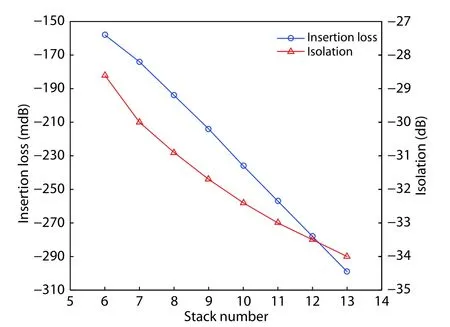
Fig. 2. (Color online) IL and isolation at 1.98 GHz vs stack number.
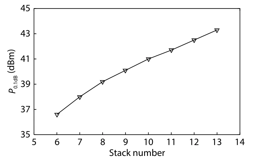
Fig. 3. Input 0.1-dB compression point at 1.9 GHz vs. stack number.

whereRonandRFETare the on-resistors of a switch branch and a single FET, respectively.Mis the stack number andRSdenotes the source impedance. The simulated performance versus stack number is shown in Figs. 2 and 3. The IL degrades while the isolation and power-handling capability get better as the stack number increases. Fig. 2 to Fig. 3 imply that the IL, isolation and power-handling capability are in trade-off relationships. To remain the same IL, sizes of multistack FETs must be multiplied, which demands larger chip area. In addition, the parasitic capacitance will increase and the high-frequency IL will degrade accordingly. Thus, the stack number is finally fixed to 9 to obtain a better overall performance while still remaining enough head- room to handle a 35-dBm input power. Considering the high-power stress is ac stress, this stack number is sufficient to deal with the antenna mismatch[5].
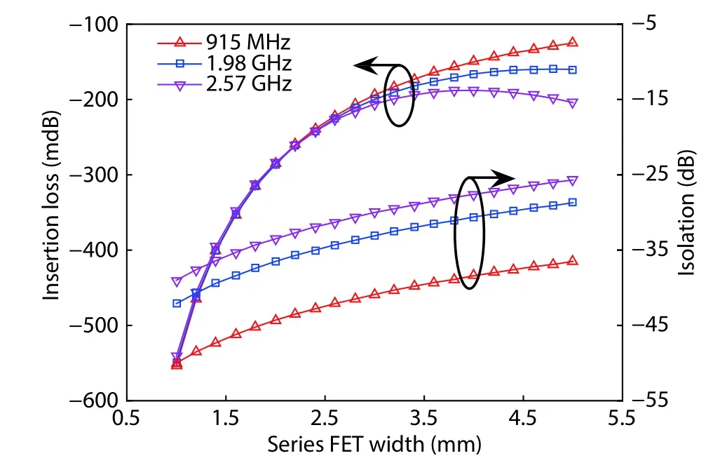
Fig. 4. (Color online) IL and isolation vs series-FET width.
The small-signal model of the SP4T switch is shown in Fig. 1 (assuming the path to RF1 is enabled). Considering the influence of off-state capacitance, the insertion loss and isolation can be expressed as:

whereβis the ratio of shunt FET width to series FET width andCoffandCshuntdenote the off-state capacitance of series branch and shunt branch, respectively. From Eqs. (6) and (7),we know that the high-frequency IL and isolation are severely degraded by the off-state capacitance, indicating there is a trade-off between the high-frequency performance and low-frequency IL when choosing the width of series FETs.Similar trade-off between isolation and high-frequency loss exists when choosing the width of the shunt FETs. The simulated insertion loss and Isolation is depicted in Fig. 4. As the series FET width increase beyond 3 mm, the IL at high frequencies shows little improvement and even gets worse. Furthermore, larger sizes of series FETs also lead to poor isolation. Considering the trade-offs above, the width of the series FETs and shunt FETs is decided to be 2.83 mm × 9 and 0.2 mm ×9, respectively.
2.2. Improved body self-biasing strategy
Biasing strategy is critical to the performance of a RF switch, especially power-handling capability. Furthermore,the design of switch controller is closely related to the biasing strategy. Several state-of-art biasing strategies have been demonstrated to ensure the implementation of superior switch performance.
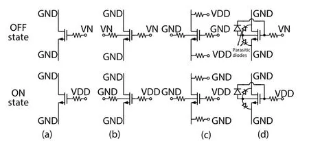
Fig. 5. Different biasing strategies. (a) Floating body FET biasing. (b) Resistive body-floating biasing. (c) DC-lifting biasing. (d) Proposed body self-biasing strategy using diodes.
Floating body FETs were used in RF switch design for its effective suppression of the leakage current to the substrate[15]. As shown in Fig. 5(a), the body contact is intrinsically a high impedance node so the leakage current to substrate is negligible. The gate is usually biased at negative voltage in the off state to enhance the power-handling capability. However, inferior harmonic performance limits its application[16].
A preferred biasing strategy is employing body-contacted (BC) FETs and a large resistor connected between the body contact and ground, which is known as resistive bodyfloating technique[14]. As shown in Fig. 5(b), the off-state leakage current to the ground is reduced by the large resistor when the parasitic diodes between drain/source and body are turned on under large voltage swing, improving the large-signal performance. A negative voltage is applied to the body and gate in the off state to optimize the power-handling capability. However, the on-state gate and body voltages are different, which demands an individual body-controlling signal and complicates the controller design.
Considering that a charge-pump-based NVG is usually necessary for negative biasing strategy and this block introduces spurious emission and increases the power consumption of the controller, an alternative dc-lifting strategy is proposed[17]. As shown in Fig. 5(c), the basic concept is to boost the dc level of the drain and source instead of applying negative voltage to the gate and body to avoid using the NVG. Nonetheless, this strategy usually needs large dc-blocking capacitors, which occupies a considerable chip area and introduces high-frequency loss. Ref. [5] demonstrates an improved dc-lifting strategy using parallel MOSFETs to reduce the dc-blocking capacitance, but this structure degrades the IL and power-handling capability.
A novel body self-biasing strategy based on diodes is employed in the proposed RF switch as an improvement of RBFT. In this structure, the large resistor connected to the body in the RBFT is substituted with a diode connected between the gate and body. As shown in Fig. 5(d), the diode is reverse biased while the drain/source-body parasitic diodes are slightly forward biased when the series/shunt branch is in on state. Therefore, most of on-state gate voltage falls on the diode, leaving the body biased at a potential close to ground. When the series/shunt branch is in off state,the diode is forward biased and turned on while the parasitic diodes are reverse biased, applying a negative voltage to the body. The main advantage of this biasing strategy is that the body is biased along with the transition of gate voltage so the controller only needs to provide the controlling signal for the gate, which simplifies the level shifters. Furthermore,the large gate resistor is reused to suppress the leakage current from the body so the chip area of around 5580μm2(95μm2× 4 × 9 + 60μm2× 4 × 9) formally occupied by the large body-connected resistors can be saved.
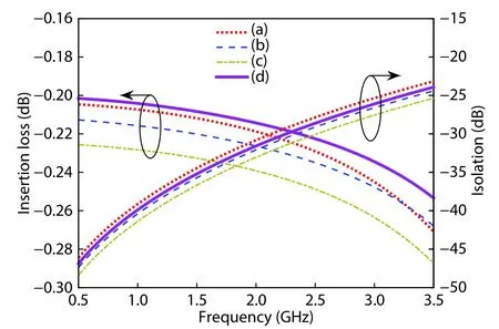
Fig. 6. (Color online) IL and isolation of different biasing strategies.

Fig. 7. (Color online) Harmonic level at 1.98 GHz of different biasing strategies.

Table 1. P0.1 dB at 1.9 GHz of different biasing strategies.
Fig. 6, Fig. 7, and Table 1 show the simulated performance of the aforementioned biasing strategies in Fig. 5. Floating-body FET biasing shows fairly good IL and isolation but its harmonic performance and power-handling capability are severely degraded by the floating-body effect. Alternative DC-lifting biasing proposed by Ref. [5] demonstrates poor IL and power-handling capability due to the existence of auxiliary FETs. Both proposed biasing strategy and resistive bodyfloating biasing show superior overall performance. Nonetheless, the controller circuitry of resistive body-floating biasing is more complicated, making proposed body self-biasing a preferable choice.
However, the turning-on voltages of the diode and the p–n junction parasitic diodes also influence the switch performance. In the on state, the dc potential of MOSFET body is lifted by around 0.22 V due to the turning-on voltage of parasitic diodes, which decreases the threshold voltage because of body effects. Therefore, the IL is improved slightly, which is verified in Fig. 6. While in the off state, the turning-on voltage of the diode decreases the absolute value of the negative voltage applied to the body, which may affect the power-handling capability. Nonetheless, Fig. 7 and Table 1 imply this degradation is minor.
Floating-body pFETs have also been used as switching devices to control the body voltage[16]. However, the floatingbody effect remains an issue, which introduces undesirable non-linearity, degrading the power-handling capability[18].A comparison of the RF switch performance is shown in Table 2, indicating the proposed biasing strategy shows better 0.1-dB compression point. Furthermore, the chip area occupied by the floating-body pFETs is almost three times that of the diodes in the 130-nm SOI CMOS process, which means the proposed biasing strategy also saves considerable chip area.
2.3. Charge-pump based controller
As depicted in Fig. 8, the switch controller consists of an oscillator with clock buffers, a charge pump, a decoder and four level shifters. A pair of input capacitors of the charge pump are charged and discharged with the differential clock signals to maintain the negative voltage at the output node,which is filtered by a capacitive load. Based on the negative voltage generated by the NVG, the level shifters convert the 4 controlling bits into 8-channel gate controlling signals toggling betweenVDDand the negative voltage to control the switch branches. Owing to the improved biasing strategy, the number of controlling signal channels is halved, which is 16 in the conventional biasing strategy, thus the design of level shifters is simplified.
The output voltage of the NVG is given by[19]:

whereCis the input capacitor,CPTis the parasitic capacitor at the top layer of the input capacitor andkdenotes the influence of theRCnetwork. The post-simulation result shows the output negative voltage is –2.43 V under a 2.8-V DC supply.
3. Measurement results
The proposed SP4T RF switch is implemented in commercial high-resistivity 130-nm SOI CMOS process. Fig. 9 shows the micrographs of the fabricated chip and the evaluation board. The total chip area including the controller, electrostatic discharge (ESD) circuitry and PADs is 0.7 × 0.7 mm2. For all the measurements, the SP4T chip is mounted and bonded onto the Rogers 4350B evaluation board. The measurement results are calibrated with the thru-line loss of the PCB traces and SMA connectors[9]. The rated operating voltage is 2.8 V and the current draw is around 120μA. Meanwhile, the measured output voltage of the NVG is –2.41 V. The logic high and low controlling voltages are 1.8 and 0 V, respectively.
Fig. 10 to Fig. 15 illustrate the measurement results while the post-simulated results are also given as comparison. The proposed SP4T switch achieves a de-embedded insertion loss of 0.27 dB/0.33 dB and an isolation of 35 dB/27 dB at 900 MHz/1.9 GHz, respectively. In the entire operating frequency band of 0.5–3.0 GHz, the measured insertion loss is less than 0.5 dB and the isolation is higher than 20 dB for allfour switch branches. The IL deviation from post-simulation is mainly caused by the bond wire with the thru-line loss calibrated. The series branches of RF1 channel and RF3 channel are closer to the ANT port and they are partly overlapped by the ANT pad (since the chip area is limited due to the packaging frame), thus increasing the off-state capacitance and leaving the isolation of corresponding channels relatively inferior. The measured output power versus input power is illustrated in Fig. 13. AP0.1dBof 38.5 dBm is achieved at 1.9 GHz.And the 2nd/3rd harmonic performance measured at fundamental frequencies of 915 MHz, 1.98 GHz and 2.57 GHz is shown in Figs. 14 and 15, indicating the 2nd/3rd harmonic is below 58 dBm/41 dBm for 35-dBm input power.

Table 2. Comparison of RF switch performance.

Fig. 8. Block diagram of the controller.

Fig. 9. (Color online) Micrographs of the fabricated chip and evaluation board.

Fig. 10. (Color online) Measured insertion loss of the SP4T switch.

Fig. 11. (Color online) Measured isolation of the proposed SP4T switch.

Fig. 12. Simulated input power compression point of the SP4T switch.
Table 2 compares the proposed SP4T switch with relevant published studies. The comparison implies the proposed SP4T switch exhibits superior insertion loss, isolation,P0.1dBas well as harmonic performance. Furthermore, the chip area is considerably reduced owing to the improved diode-based biasing strategy.
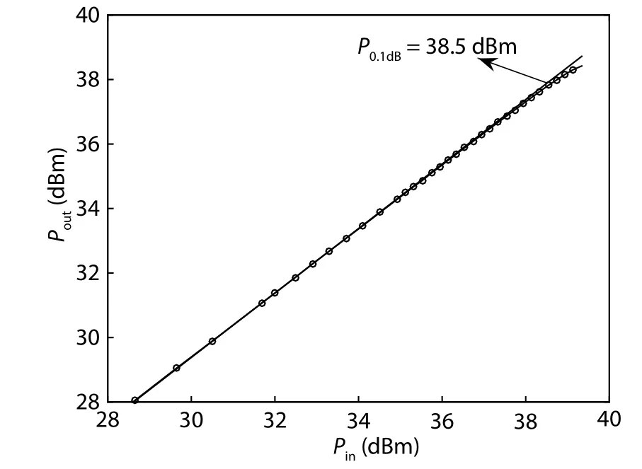
Fig. 13. Measured input power compression point of the SP4T switch.
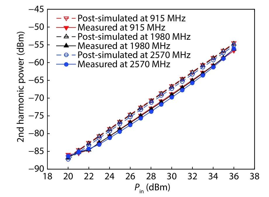
Fig. 14. (Color online) Measured 2nd harmonics of the SP4T switch.

Fig. 15. (Color online) Measured 3rd harmonics of the SP4T switch.
4. Conclusion
In this paper, an ultra-low loss and high-linearity SP4T RF switch using multistack FET architecture is proposed.With diode-based body self-biasing strategy employed in the topology, the circuitry of controller is simplified while maintaining superior power-handling capability. Overall performance is ensured by optimizing the stack number and device sizes. The proposed switch exhibits an insertion loss less than 0.5 dB and an isolation higher than 20 dB up to 3 GHz and demonstrates a 0.1 dB compression point of 38.5 dBm. The chip area is only 0.49 mm2. With excellent performance over the frequency band from 0.5–3.0 GHz, this RF switch can be used in GSM, WCD-MA and LTE bands.
Acknowledgements
The major work is performed at MESIC (a joint lab of USTC and IMECAS) and Hengxin Semitech Co., Ltd., and partially carried out at the USTC Center for Micro and Nanoscale Research and Fabrication. The authors would also like to thank the Information Science Laboratory Center of USTC for software & hardware services.
杂志排行
Journal of Semiconductors的其它文章
- S uppression of oxygen and carbon impurity deposition in the thermal system of Czochralski monocrystalline silicon
- A snapback-free and high-speed SOI LIGBT with double trenches and embedded fully NPN structure
- Wireless communication and wireless power transfer system for implantable medical device
- Defect levels in d-electron containing systems: Comparative study of CdTe using LDA and LDA + U
- Comparative study of various methods for extraction of multiquantum wells Schottky diode parameters
- 4H-SiC trench MOSFET with an integrated Schottky barrier diode and L-shaped P+ shielding region
