Recent Progress in Photocatalytic Hydrogen Evolution
2020-03-27JinboPanShengShenWeiZhouJieTangHongzhiDingJinboWangLangChenChakTongAuShuangFengYin
Jinbo Pan , Sheng Shen , Wei Zhou , Jie Tang , Hongzhi Ding , Jinbo Wang , Lang Chen ,Chak-Tong Au , Shuang-Feng Yin ,*
1College of Chemistry and Chemical Engineering, State Key Laboratory of Chemo/Biosensing and Chemometrics, Provincial Hunan Key Laboratory for Cost-effective Utilization of Fossil Fuel Aimed at Reducing Carbon-dioxide Emissions, Hunan University,Changsha 410082, P. R. China.
2 College of Chemistry and Chemical Engineering, Hunan Institute of Engineering, Xiangtan 411104, Hunan Province,P. R. China.
Abstract: The photocatalytic hydrogen evolution reaction (PHER) has gained much attention as a promising strategy for the generation of clean energy. As opposed to conventional hydrogen evolution strategies (steam methane reforming, electrocatalytic hydrogen evolution, etc.), the PHER is an environmentally friendly and sustainable method for converting solar energy into H2 energy. However, the PHER remains unsuitable for industrial applications because of efficiency losses in three critical steps: light absorption, carrier separation, and surface reaction. In the past four decades,the processes responsible for these efficiency losses have been extensively studied. First, light absorption is the principal factor deciding the performance of most photocatalysts, and it is closely related to band-gap structure of photocatalysts.However, most of the existing photocatalysts have a wide bandgap, indicating a narrow light absorption range, which restricts the photocatalytic efficiency. Therefore, searching for novel semiconductors with a narrow bandgap and broadening the light absorption range of known photocatalysts is an important research direction. Second, only the photogenerated electrons and holes that migrate to the photocatalyst surface can participate in the reaction with H2O,whereas most of the photogenerated electrons and holes readily recombine with one another in the bulk phase of the photocatalysts. Hence, tremendous effort has been undertaken to shorten the charge transfer distance and enhance the electric conductivity of photocatalysts for improving the separation and transfer efficiency of photogenerated carriers. Third,the surface redox reaction is also an important process. Because water oxidation is a four-electron process, sluggish O2 evolution is the bottleneck in photocatalytic water splitting. The unreacted holes can easily recombine with electrons.Sacrificial agents are widely used in most catalytic systems to suppress charge carrier recombination by scavenging the photogenerated holes. Moreover, the low H2 evolution efficiency of most photocatalysts has encouraged researchers to introduce highly active sites on the photocatalyst surface. Based on the abovementioned three steps, multifarious strategies have been applied to modulate the physicochemical properties of semiconductor photocatalysts with the aim of improving the light absorption efficiency, suppressing carrier recombination, and accelerating the kinetics of surface reactions. The strategies include defect generation, localized surface plasmon resonance (LSPR), element doping,heterojunction fabrication, and cocatalyst loading. An in-depth study of these strategies provides guidance for the design of efficient photocatalysts. In this review, we focus on the mechanism and application of these strategies for optimizing light absorption, carrier separation and transport, and surface reactions. Furthermore, we provide a critical view on the promising trends toward the construction of advanced catalysts for H2 evolution.
Key Words: Photocatalysis; Hydrogen evolution; Light absorption; Carriers separation; Surface reaction
1 Introduction
With the advantages of high energy density, wide source range and environmental friendliness, hydrogen (H2) is considered as one of the most ideal alternatives to fossil fuels1. However, it is mostly generated through thermal processes such as steam reforming and gasification of fossil fuel, which defeats the purpose of cutting down the reliance on fossil fuel. Hence, it is imperative to develop alternative routes for H2formation from energy resources that are renewable. As a sustainable method for H2production, the photocatalytic splitting of water for H2evolution has been investigated worldwide in recent years2-4.
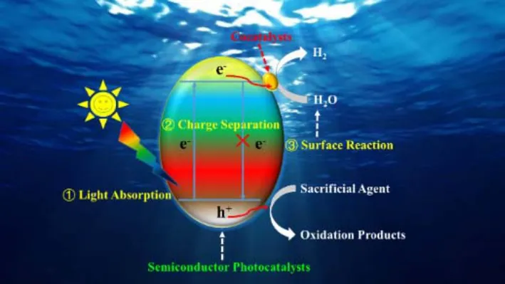
According to the energy band theory of solids, when the energy of incident photon is larger than the band gap of a semiconductor photocatalyst, electrons can be excited from the valence band (VB) to the conduction band (CB), generating photo-induced holes and electrons in the VB and the CB,respectively. The holes with oxidizing ability can react with OHfrom water to produce O2, while the electrons with reducing ability react with H+to generate H25. Fig. 1 is the schematic depicting the basic principles of water splitting on a semiconductor photocatalyst. The redox ability of holes and electrons are dictated by the relative position of VB and CB.Specifically, photocatalytic water splitting is thermodynamically feasible when the CB minimum of the photocatalyst is more negative than the redox potential of H+/H2(0 VvsNHE, pH =0), while the VB maximum is more positive than the redox potential of O2/H2O (1.23 VvsNHE, pH = 0)6. Semiconductors that satisfy this strict requirement while having efficient light absorption, decent charge-carrier separation and enough kinetic overpotential to drive the reaction are rare, and modification of common photocatalysts is almost inevitable. Thus a close look into the key limiting factors during the catalytic process is critical for rational design and tailoring of photocataysts.
There are five major steps in photocatalytic water splitting: (i)reactant adsorption on the surface of a photocatalyst, (ii) light absorption by the photocatalyst to generate electron-hole pairs,(iii) separation and migration of electrons and holes from bulk to surface, (iv) surface reactions for the reduction and oxidation of water, (v) product desorption from the catalyst surface7. Among them, steps ii-iv are the most extensively studied because they dictate the efficiency of the overall reaction. These key steps in photocatalytic processes are shared by all photocatalytic materials, and hence provide universal guidelines for efficiency improvements.
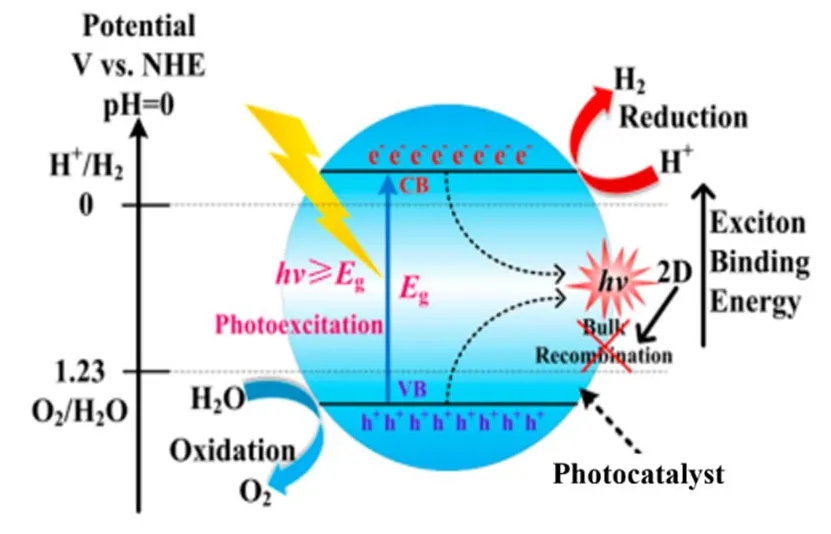
Fig. 1 Schematic showing the basic principles of photocatalytic water splitting.
Light absorption of semiconductor determines the upper limit of photocatalytic efficiency and is closely related to the band gap by the equationλ= 1240/Eg, whereλis the light absorption edge andEgis the band gap of the semiconductor8. A narrower band gap would mean stronger light absorption, but it compromises the driving force for the reaction. Once the electron-hole pairs are successfully generated upon photon absorption, electrostatic force compels them to recombine whenever possible9,10. Both bulk and surface recombination could deactivate the excitons and diminish the efficiency of the water splitting process11. It is worth noting that for two semiconductors with similar light absorption, the carrier mobility and diffusion length can be vastly different. The increase of exposed surface area and shortening of diffusion length are beneficial for reducing bulk recombination. Recombination inhibitors or built-in electric field are also necessary to drive the efficient flow of the electrons and holes12,13. Once the excitons have made their way to the surface and are in contact with the reactant, the redox reaction is triggered at the respective photocatalytic active sites14-16. The sluggish water oxidation half reaction is the rate-determining step with the undesired O2as by-product. Sacrificial reagents(typically sulfides, sulfites, thiosulfates, alcohol or amines) are often added to consume the holes in a timely fashion and accelerate the hydrogen generation rate17. The lifetime of the charge carriers is in nanoseconds while the water reduction takes place in milliseconds. The mismatched time scale between the two consecutive steps demands efforts in either prolonging the lifetime of the charge carriers,viz.promoted charge separation or accelerating the reaction. The use of cocatalysts (including those of noble metals and non-noble metals) to promote water splitting has been confirmed to be effective18. In this article,recent progresses of photocatalytic water splitting have been systematically reviewed, focusing on the three key steps of the photocatalytic process described above: light absorption, charge separation and surface reactions. Furthermore, the mechanisms of the strategies employed for performance improvement are discussed, along with the challenges and opportunities for future development and breakthrough. It is believed that an in-depth review of this kind could provide guidance for the design and fabrication of state-of-the-art photocatalysts that are highly efficient for the conversion of solar energy by means of water splitting.
2 Semiconductor photocatalysts for H2 generation
Semiconductors have an essential role to play in the photocatalysis of water splitting. Photocatalytic efficiency is closely related to the physicochemical property of the semiconductor materials. For example, semiconductor photocatalysts with different band gap structures are distinct in light absorption ability as well as specific in the reaction that could be catalyzed. Furthermore, the morphology of a photocatalyst can dictate its specific surface area, affecting reactant adsorption and product desorption as a result. The combination of two or more semiconductors could lead to synergistic effects in catalyzing reactions that might not otherwise be feasible by a single component. It is apparent that a skillful deployment of specific strategies may have positive effects on the performance of photocatalysts.
After four decades of hard work, remarkable advances have been made in the research of efficient photocatalysts for H2evolution, including TiO211,19, WO320,21, MoS222,23, CdS6,10, g-C3N424,25, Cu2O26,27, ZnIn2S428-30, CdIn2S431,32. Fig. 2 shows the band gap energy as well as the VB and CB energy levels of the commonly used semiconductors for H2evolution relative to the water redox potentials. Despite the semiconductors with wide band gaps (such as TiO2) straddle the water redox potential,they have low solar-to-H2conversion efficiency because they could not utilize visible light. On the other hand, semiconductors with narrow band gaps (such as Cu2O) have strong visible light absorption ability but are poor in oxidation ability. Even for two semiconductors with similar CB and VB positions, the configuration of electronic structure and shape of the bands can make a difference in light absorption and charge transfer. In theory, semiconductor photocatalysts with sufficiently positive VB (VB > 1.23 VvsNHE) and sufficiently negative CB (CB <0 Vvs NHE) can achieve overall water splitting for H2generation33. In reality, however, most of the photocatalysts that straddles the water redox potential are not capable of realizing overall water splitting owing to poor charge transfer efficiency and high energy barrier of the redox reaction. Taking into account the thermodynamics and kinetics losses, the band gap of a semiconductor photocatalyst should be over 1.9 eV for overall water splitting34. Therefore, efforts been made to optimize light absorption, charge transfer and redox reaction kinetics of semiconductor photocatalysts as illustrated in Table 117,35-51.
3 Light absorption
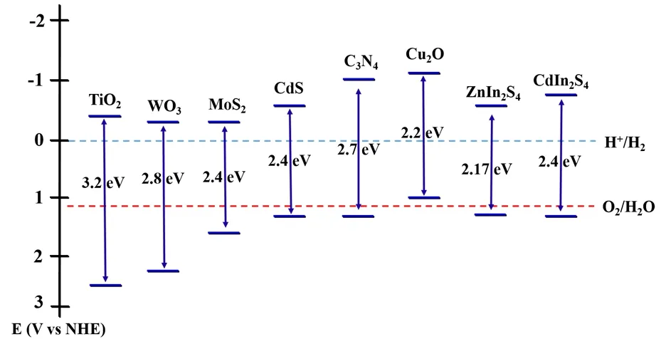
Fig. 2 Band gap energy and VB and CB positions of selected photocatalysts for H2 evolution.
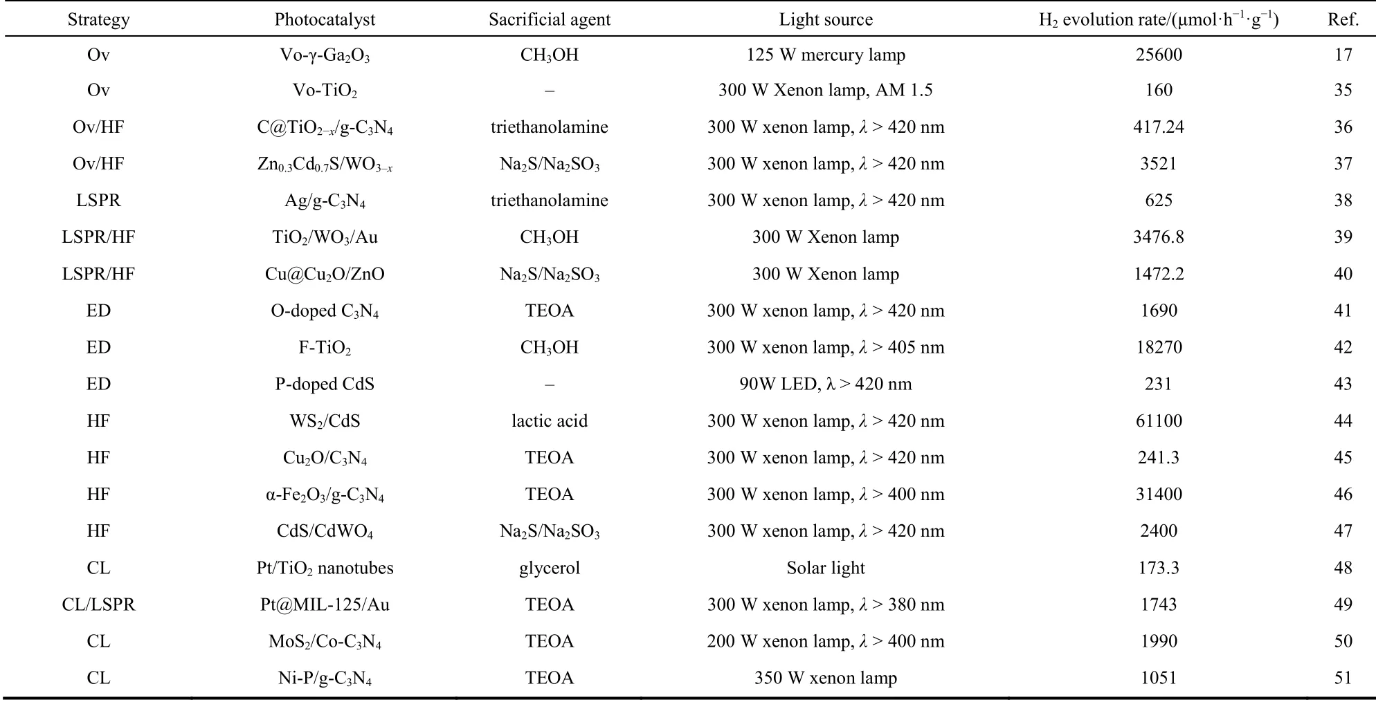
Table 1 Summary of the strategies for photocatalytic H2 evolution.
The PHER is initiated by light absorption. Therefore, the performance of a photocatalyst is first restricted by its light absorption capacity5, which is closely related to the band structure. As a result of the efforts made in the past decade,several common approaches have been adopted to enhance light absorption, particular visible-light absorption since it accounts for almost half of the solar spectrum while UV light accounts for only less than 5%. Through the tuning of band gap, it is possible to achieve high light absorption. It is known that quite a number of physical properties of semiconductors are under the influence of defects, including optical absorption, electrical conductivity,carrier diffusion kinetics and thermoelectric power52. Defect formation in crystal lattice in real practices is unavoidable because it leads to structure disorder and increase of entropy.Defects in photocatalytic materials can be divided into four main categories according to dimensions: zero-dimensional point defects such as vacancies and dopant nanoparticles; onedimensional line defects such as screw and edge dislocation;two-dimensional planar defects such as grain boundary and twin boundary, and three-dimensional volume defects such as lattice disorder and void53. With relatively lower formation energy on oxide surfaces, the generation of oxygen vacancies is the most prevalent and has been widely studied. With the missing of an oxygen atom, the electron pairs that remain trapped in the lattice give rise to a color center: lattice defects that absorb visible or infrared light. The weakened bonding at the defect site reduces splitting between the bonding and antibonding orbitals, creating discrete electronic states within the band gap. These electronic states narrow the bandgap or act as midgap states for the photoexcited electrons. The enabled defect-to-CB transitions and the VB-to-defect transitions extend the absorption edge to longer wavelengths. The level of the midgap states could be tuned from shallow to deep by varying the density of the oxygen vacancies54.
Oxygen vacancies (Ov) can be generated by hydrogen/nitrogen thermal treatment55,56, plasma etching57, or under reaction conditions58. Among them, hydrogen treatment was considered as an easy way to create oxygen vacancies without dopants59. Hydrogen is a strong reducing agent capable of reducing metal oxides and generating oxygen vacancies at elevated temperatures. As early as the 1950s, hydrogen treatment was applied to create oxygen vacancies in TiO2. It was reported that the hydrogen treatment could cause a shift of light absorption from ultraviolet to infrared region60. Later Chenet al.61prepared black TiO2nanoparticles by annealing TiO2in a H2atmosphere of 2 MPa at about 200 °C for 5 days. As shown in Fig. 3A, the color of the TiO2changed from white to black after the hydrogen treatment, indicating that the presence of oxygen vacancies could significantly affect the band gap of TiO2.Compared with the untreated TiO2, the black TiO2with disordered surface showed improved visible-light absorption ability (Fig. 3B-D), and exhibited enhanced photocatalytic performance for hydrogen evolution in the presence of sacrificial agents. Plasma etching has also been proved to be an effective way to induce oxygen vacancies in photocatalysts62. Recently,Konget al.57reported the preparation of ultrathin TiO2nanosheets with abundant oxygen vacancies by means of plasma engraving. As shown in Fig. 4a, the color of the TiO2transformed from white into yellow after plasma etching, along with changes in molecular structure. Introducing of oxygen vacancies can also promote the formation of defect states (the red line in Fig. 4b) below the original CB minimum. Compared with the untreated TiO2, the yellow TiO2has narrower band gap and highly improved light absorption ability, which are beneficial for PHE activity. Ideally the concentration and distribution of oxygen vacancies can be tuned by varying the reduction time, temperature and/or rate of hydrogen flow.However, it is difficult to quantify and map the location of oxygen vacancies in semiconductor photocatalysts. It is important to note that excess vacancies can introduce midgap states too close to the VB, which could be detrimental for photocatalytic performance because the midgaps could act as recombination centers for electron-hole pairs.

Fig. 3 (A) Photographic image, (B) UV-Vis absorption diffuse reflection spectra (DRS), and HRTEM image of(C) white TiO2 nanocrystals and (D) black TiO2 nanocrystals with disorders.

Fig. 4 (a) Preparation route and the molecular structure, (b) schematic of energy band structures, and(c) UV-Vis DRS spectra of pristine and plasma treated TiO2.
Another method for extending light absorption is through coupling with metal nanostructures as tunable light antennas.When photocatalysts are decorated with metal nanoparticles that are less than 30 nm in size, there is improvement of light trapping efficiency due to light confinement and/or scattering63,64. The electromagnetic field from the incident light exerts a force on the free electron gas in the metal conduction band, causing them to oscillate collectively. If the frequency of the incident light matches that of the free charges of metal particles, a strong oscillation of surface electrons occurs. As shown in Fig. 5, this phenomenon is called “localized surface plasmon resonance(LSPR)”33,65. The LSPR wavelength is defined as the wavelength that causes oscillation amplitude to reach a maximum. The plasmon-induced light harvesting at metal/semiconductor heterostructure interfaces is prominently beneficial for enhancing the reactivity of a photocatalytic system66. Methods, such as vacancy introduction, manipulate light harvesting through band-gap tuning and introduction of electronic states in the forbidden band, which can cause unintended results such as lowering of driving force for redox reaction or increased charge recombination. The use of LSPR,however, does not compromise the physiochemical properties of the photocatalyst, but extends light absorption and improves carrier transport. The Schottky contact of plasmonic metal and semiconductor greatly prolongs the lifetime of hot carriers generated as a result of metal excitation. By varying the size,shape, and composition of the plasmonic metal, the light absorption range can be tuned across the visible to near-infrared region. Semiconductor photocatalysts of wide band gaps, such as TiO2and C3N4, exhibit enhanced light absorption ability and excellent activity for H2evolution when coupled with plasmonic metals.
Recently, Gaoet al.67synthesized TiO2/WO3electrospun nanofibers decorated with Au nanoparticles that led to significant broad-band light absorption. As shown in Fig. 6a-c,the Au nanoparticles dispersed evenly on the surface of TiO2,significantly enhancing light absorption from 400 to 800 nm while promoting charge transfer. The TiO2/WO3/Au-0.45%photocatalyst showed a significantly improved H2production rate of 269.63 μmol·h-1. This study suggests that through coupling with plasmonic materials for the adjustment of composition, morphology, and even dielectric properties of a photocatalyst, it is possible to maximize the absorption of solar energy. Moreover, by a supramolecular hydrogel pyrolysis approach, Wanget al.68decorated porous g-C3N4nanofibers with Ag nanoparticles (size < 10 nm) for photocatalytic hydrogen generation (Fig. 7). With the presence of plasmonic Ag, the light absorption ability of g-C3N4was greatly improved in both the ultraviolet and visible region, leading to excellent photocatalytic H2generation activity. It has been well documented that the integration of plasmonic materials with photocatalysts is an effective way to extend the light absorption range for better conversion of solar energy to chemical energy.Simply mixing a plasmonic metal with a semiconductor or random depositing a plasmonic metal on a semiconductor would result in weak interaction between the metal and the photocatalyst, leading to poor electron transfer between the two partners, and likely no improvement of solar energy conversion.The postulated active sites are located at the interface between the metal and the semiconductor; thus the interfacial structure and charge distribution at the interface deserve close investigation. It is important to note that some plasmonic metals,such as Au and Pt, can also act as a cocatalyst, giving the added benefits of surface catalysis, surface passivation and/or Fermi level equilibration effects. Therefore, the role of a plasmonic metal must be scrutinized to make sure that the performance improvement is due to plasmonic effect.
The above strategies can significantly improve light absorption of semiconductor photocatalysts from UV light region to visible light region. However, solar spectrum is constituted by more than 50% near-infrared (NIR) light, 42%-45% visible light and 5% UV light69,70. Taking full advantage of NIR light will tremendously improve the conversion efficiency of sunlight. Recently, researchers discovered that upconversion nanoparticles (UCNPs) can absorb NIR photons and emit UV and visible emissions, which is called upconversion effect.Because of their unique optical properties, the UCNPs have been adopted to broaden the light absorption of photocatalysts.NaYF4:Yb3+, Tm3+is a typical upconversion luminescence material for NIR light to UV light70. Upconversion is a multiphoton process in which NIR light is converted to higher energies from the deep UV to the NIR by successive energy transfer processes.
Liet al.71constructed a UCNPs-Pt@MOF/Au heterojunction photocatalyst, where MOF is mostly responsive to UV light, the plasmonic Au absorbs visible light, meanwhile the UCNPs upconvert NIR light to UV and visible light, which are harvested by the MOF and Au once again, giving rise to light harvesting from UV to NIR region, as shown in Fig. 8. Moreover, the MOF realizes the spatial separation for Au and Pt NPs, enables catalytic substrates/products accessible to Pt active sites, and also facilitates the generation of Au NPs for light absorption. The results indicate that UCNPs-Pt@MOF/Au exhibits broadband photoresponse from UV to NIR region, as well as much enhanced photocatalytic hydrogen evolution activity with the rate of 280 μmol·g-1·h-1. These spectral changes reflect the energy transfer between UCNPs and MOF as well as Au NPs,resulting in the effective utilization of NIR light by MOF and Au NPs based on the inherent upconversion mechanism.

Fig. 8 (a) The light absorption of each component in the composites and the mechanism for photocatalytic hydrogen production,(b) schematic illustration of synthetic process for the UCNPs-Pt@MOF/Au composites.
4 Carriers separation
During PHE reactions, the recombination of photogenerated electrons and holes occurs in the bulk as well as on the surface of photocatalysts4, leading to poor photocatalytic performance.It has been reported that the apparent charge separation efficiency of a photocatalyst can be associated with charge generation as well as charge transfer efficiency72,73. Numerous methods have been explored to improve the separation and transfer efficiency of photogenerated electrons and holes.Element doping is known for a long time to be an effective method to tune the electronic structure of photocatalysts and accelerate the separation of electron-hole pairs by adding electronic states in the forbidden band74-76. The doped atoms/ions with the ability to trap electrons and holes can serve as recombination inhibitors. The charge carrier mobility can also be tuned by bulk doping. The mobility of holes is governed by the width of VB; a wider VB suggests higher hole mobility77.Homogeneous bulk doping can effectively elevate the VB maximum by mixing dopant states with the existing upper VB states in a bulky semiconductor. Metal (e.g., K, Na, Fe, Cu, and W) and nonmetal (e.g., P, S, C, I, and B) elements were incorporated into the framework of photocatalysts to enhance the charge transfer efficiency and photocatalytic performance for hydrogen generation44,78. These dopant ions/atoms can be placed in the host lattice by replacing the existing ions/atoms or staying at the interstitial positions of lattice. It should be noted that the radii of substitutional atoms/ions should match those of the replaced atoms54. What’s more, vacancies and nonstoichiometric compositions are often termed “self-doping”, for example TiO2with oxygen vacancies can be viewed as TiO2doped with Ti3+.
According to previous researches the degree of doping is dependent on the doping method as well as on the structure of the doped materials. For instance, Liet al.reported the hydrothermal treatment of mesoporous and solid spherical TiO2precursors with ammonia followed by heating at 400 °C79. The results indicate that N can be uniformly doped into the mesoporous TiO2spheres from surface to bulk, but only into the subsurface of the closely packed solid TiO2spheres. These phenomena suggest that the structure of a semiconductor could significantly affect the distribution of dopants. Hierarchical photocatalytic materials with interlayer galleries are another class of structures in which homogeneous distribution of a dopant can be easily realized throughout the entire semiconductor matrix. Recently, Zhuet al.80synthesized Pdoped g-C3N4with in-plane mesopores by co-condensation of melamine and (hydroxyethylidene)diphosphonic acid. As shown in Fig. 9, the N atoms in the skeleton of flower-like g-C3N4nanostructure are partially replaced by P atoms, indicating that the P species can not only chemically bond with the C and N, but also achieve planar coordination in the g-C3N4framework. With the delocalization of lone electron pairs into theπ-conjugated tris-triazine of P-doped g-C3N4, there is enhancement of conductivity and charge transfer efficiency, significantly promoting the overall H2evolution performance. It is worth noting that doping is essentially a deliberate act of introducing defects and the nature of defects in microscopic scale can be rather complicate. To maintain electroneutrality, deformation of lattice structure is likely to occur in the presence of dopants. It is important to distinguish whether the performance improvement is caused by the dopant itself or solely by lattice distortion.Doping with certain elements may have nil or even negative effects on photocatalytic performance because they could act as recombination centers instead of inhibitors. Thus careful selection of dopant and control of dopant concentration is essential to achieve charge separation efficiency.

Fig. 9 (a) The morphology and molecular structure of P-doped g-C3N4; (b) PHE over P-doped g-C3N4 (i), g-C3N4 nanosheet (ii),mesoporous g-C3N4 (iii), and g-C3N4 (iv); and (c) photoluminescence spectra and (d) photocurrent response of P-doped g-C3N4 and g-C3N4.

Fig. 10 Schematic of (a) the generation and recombination process of electrons and holes in a photocatalyst, (b) Type-I heterojunction,(c) Type-II heterojunction and (d) Direct Z-scheme system.
Heterojunction fabrication is another promising strategy for separation promotion of photogenerated electron-hole pairs.Heterojunctions created by assembling two hotocatalysts (PC I and PC II) are often held together by chemical bonds,electrostatic force or mechanical force and the interface plays a key role in ensuring fast transfer of charge carriers. A large contact area and low degree of lattice mismatch are highly desirable in the construction of heterojunctions. The difference in work function between two semiconductors induces electron redistribution and the formation of a built-in electric field, which drives electron-hole separation and suppresses recombination.Semiconductor heterojunctions can be divided into three categories (Fig. 10): Type-I heterojunction (straddling), Type-II heterojunction (staggering), and Z-scheme heterogjunction81,82.For Type-I heterojunction, when both photocatalysts are excited by an incident light, the electrons of PC II with higher CB position migrate to PC I with lower CB position under the force of electrostatic field. Meanwhile, the photogenerated holes transfer from the lower VB position to the higher VB position.Finally, both the photogenerated electrons and holes are accumulated on PC I. In the case of Type-II heterojunction, the transfer of electrons is similar to that of Type-I heterojunction,from PC II to PC I. However, the migration of holes follows a reverse trend, from PC I to PC II. In this case, the photo-induced electrons are accumulated on PC I for reduction reaction while holes on PC II for oxidation reaction. By guiding the flow of electrons and holes at the interface, the creation of heterojunction can result in enhancement of charge separation,and the suppression of charge recombination would significantly improve photocatalytic activity.

Fig. 11 (A) Schematic of the structure and photocatalytic process of WS2-CdS, (B) graphical representation of visible-light induced charge transfer between CdS and WS2, (C) time-dependent PHE for prepared samples, (D) photocurrent responses of (a) purchased WS2,(b) CdS NRs, and (c) WC-1.6 electrodes.
Heet al.43reported the modification of CdS nanorods with WS2nanosheets (Type-I heterojunction) by an ultrasonic/exfoliation method using dimethylformamide as dispersing agent (Fig. 11). The configuration with widespread heterojunctions displayed well-matched band alignment for efficient charge transfer and excellent PHE activity. Because WS2has a lower CB but a higher VB than CdS, the photogenerated electron-hole pairs easily transfer from CdS to WS2, resulting in efficient separation. Furthermore, the flow of charge carriers at the heterojunctions effectively eliminates the accumulation of holes on CdS nanorods, inhibiting photocorrosion and prolonging the stability of the photocatalyst.Compared with pure CdS, WS2/CdS with a H2evolution rate of 1222 μmol·h-1(20 mg of catalyst) is significantly higher in activity. Chenet al.45reported the modification of g-C3N4with Cu2O nanoparticles (Type-II heterojunction)viaa one-potin situreduction method. As shown in Fig. 12, there is uniform distribution of Cu2O nanoparticles with size less than 10 nm on the surface of g-C3N4. Also, the widespread heterojunctions and the staggered band structure between Cu2O and g-C3N4enable efficient transfer of photo-generated charge carriers. The hydrogen evolution rate improved from 141.6 μmol·h-1·g-1of pure g-C3N4to 241.3 μmol·h-1·g-1of Cu2O/g-C3N4, showing an enhancement of up to ~70%. Overall, the results of Heet al. and Chenet al.demonstrate that the construction of Type-I and Type-II heterojunctions can effectively increase the charge transfer efficiency, thereby improve the photocatalytic activity of semiconductor photocatalysts.
Nonetheless, because of the partial loss of redox ability during electron-hole transfer, there is weakening of driving force at Type-I and Type-II heterojunctions that may lead to failure of a specific photocatalytic reaction83. Compared with Type-I and Type-II heterojunctions, the biomimetic configuration of Zscheme photocatalysts has been proved to be photocatalytically more efficient46,84. In a typical direct Z-scheme pathway, the photogenerated electrons with strong reducing ability in the CB of PC I and holes with strong oxidizing ability in the VB of PC II are preserved, while the photogenerated electrons in the CB of PC II and holes in the VB of PC I with inferior redox power recombine85,86. As a result, a Z-scheme photocatalyst is endowed with strong redox ability while having the reductive and oxidative active sites spatially separated, allowing water oxidation and reduction on a single photocatalyst87. This unique benefit enables the conjunction use of a half-reaction catalyst in hydrogen evolution similar to that in a photoelectrochemical setup for water splitting. Recently, Sheet al.46synthesized a Zscheme α-Fe2O3/g-C3N4photocatalystviaa solvothermalpyrolysis method. As shown in Fig. 13, the all-solid-state Zscheme structure is composed ofn-type α-Fe2O3nanosheets andn-type 2D g-C3N4in direct and close contact. The heterojunctions and the match of band gap structure allow efficient transfer of photoexcited electrons to the reactant.Meanwhile, the electrons in the CB of g-C3N4with strong reduction ability are maintained. The optimized α-Fe2O3/g-C3N4exhibits unprecedented PHE activity, achieving a rate of 31400 μmol·g-1·h-1and a remarkably high external quantum efficiency of 44.4% at a wavelength of 420 nm. Nonetheless, both Type II heterojunctions and direct Z-scheme structure involve direct contact and electron transfer between two semiconductors without a mediator, and the exact mechanisms can sometimes be ambiguous. It is hence necessary to provide directin situevidence of electron-hole transfer paths based on high-timeresolution techniques before making a claim on Z-scheme structure.
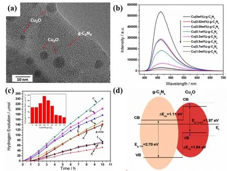
Fig. 12 (a) TEM images of Cu(0.5wt%)/g-C3N4, (b) photoluminescence spectra of samples, (c) PHE under visible-light irradiation,(d) energy band alignment of Cu2O/g-C3N4 heterojunction

Fig. 13 (a) Synthesis and structure of the nanostructures and hybrids, (b) photoluminescence of ML g-C3N4 (blue),α-Fe2O3/ML g-C3N4 (green), 2D g-C3N4 (pink), and α-Fe2O3/2D g-C3N4 hybrid (3.8%, red), (c) PHE of samples, and(d) energy band diagram of Z-scheme mechanism of α-Fe2O3/2D g-C3N4.

Fig. 14 (a) HRTEM image of TiO2-Au-CdS, (b) energy band diagram scheme of the CdS-Au-TiO2 system.
Owing to the lattice mismatch and the large interface resistance between two semiconductors, transfer efficiency of the photogenerated electrons-holes are seriously hampered.Hence, it is a challenge for accelerating the charge transfer at the interface of heterojunction. Noble metals as cocatalyst can enhance the separation of charge carriers. The noble metals in the photocatalyst-noble metal-photocatalyst systems show generally the stronger ability for charge transfer than in the case of the solid-solid contact interface in the photocatalystphotocatalyst systems due to the difference in their electrical resistances88,89. Au was first adopted as the conductor to construct Z-scheme TiO2-Au-CdS system in 200690, as shown in Fig. 14. Owing to the rapid photogenerated electrons transfer from the CB of TiO2to the VB of CdS through Au NPs, the resulting Z-scheme TiO2-Au-CdS system exhibits higher photocatalytic H2evolution activity than the two-component Au-TiO2and TiO2-CdS systems.
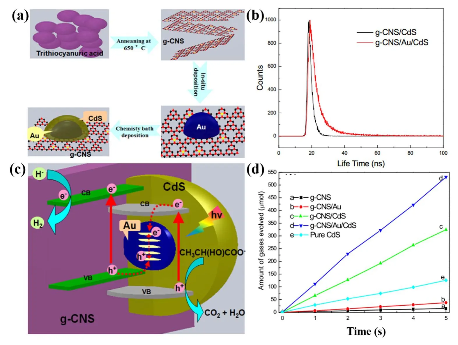
Fig. 15 (a) Schematic illustration of the relevant preparation process, (b) excited state electron radioactive decay, (c) proposed mechanism for Z-scheme charge-carrier transfer process, (d) photocatalysis hydrogen evolution ability of the as prepared samples.
Au nanoparticles can link not only two inorganic semiconductors, but also inorganic semiconductor and inorganic semiconductor. Recently, Liet al.91reported a Z scheme g-C3N4/Au/CdS photocatalyst, in which the surface-coated Au nanoparticles with CdS were uniformly dispersed on the surface of g-C3N4nanosheets. As shown in Fig. 15, two-step selfassembly process was used to construct regional sandwichstructured Z-scheme g-C3N4/Au/CdS photocatalyst. Efficient charge transfer at interface of g-C3N4/Au/CdS endow the photoelectron longer lifetimes with 55.6 ns, compared with g-C3N4(28.1 ns). This reason can be ascribed to the excellent electrical conductivity of Au, accelerating the charge transfer between g-C3N4and CdS. The photocatalytic activity showed that ternary heterojunction photocatalyst possesses much higher hydrogen evolution activity than binary and single photocatalyst,which indicates that embedded Au nanoparticles constructed the Z-scheme mechanism of g-C3N4/Au/CdS photocatalyst. The oxidation/reduction ability of photogenerated holes and electrons were enhanced.
Based on the research results above, it is safe to conclude that heterojunction fabrication can effectively promote the separation of photogenerated charge carriers while selectively utilizing the strong driving force originated from the two semiconductors. Especially, noble metals can effectively enhance the separation of charge carriers. Meanwhile, the embedded noble metals nanoparticles between two semiconductor photocatalysts can provide new electron transfer paths. More importantly, the design strategies provide inspiration and guideline for the construction of advanced photocatalytic systems by tailoring the band gap structure of photocatalysts for specific redox reactions.
5 Surface reaction
What is occurring on the surface of a photocatalyst is decisive.With the separation and migration of photoinduced electrons and holes to the surface, redox reactions are triggered. It has been reported that surface reactions are rate determining in catalytic processes92,93. Most of the semiconductor photocatalysts suffer from sluggish surface reactions for water splitting, which results in the accumulation of hot electrons and holes on the surface of photocatalysts. The outcome is charge recombination and photocorrosion of photocatalysts94,95.
It was observed that the presence of a cocatalyst such as Pt,MoS2, CoS2or NiS could significantly accelerate the water splitting process. Generally speaking, a cocatalyst should have one or more of the following functions: providing reduction or oxidation active sites, lowering activation energies, trapping charge carriers, suppressing charge carrier recombination96. The water reduction and oxidation reaction often require different cocatalysts, and they can be used separately or in conjunction for the promotion of water splitting. The photocatalytic generation of H2involves two basic surface reactions: proton reduction with e-and oxidation of electron donors with h+18. The reduction of protons in the presence of a cocatalyst can be divided into three steps: (i) the cocatalyst traps electrons from the light-harvesting semiconductor; (ii) H+accepts an electron and is reduced to H atom; and (iii) two surface H atoms unite to form a H2molecule.H* (where * denotes a site on the cocatalyst surface) as the catalytic intermediate plays an important role in PHER, which may occur through either the Volmer-Heyrovsky or the Volmer-Tafel mechanism97. The rate of the overall reaction is largely determined by the hydrogen adsorption free energy, ΔGH. If hydrogen binds to the surface too weakly, the adsorption(Volmer) step will limit the overall reaction rate, whereas if the binding is too strong, the desorption (Heyrovsky/Tafel) step will limit the rate. Thus, a necessary but insufficient condition for an active HER catalyst is ΔGH≈ 0.
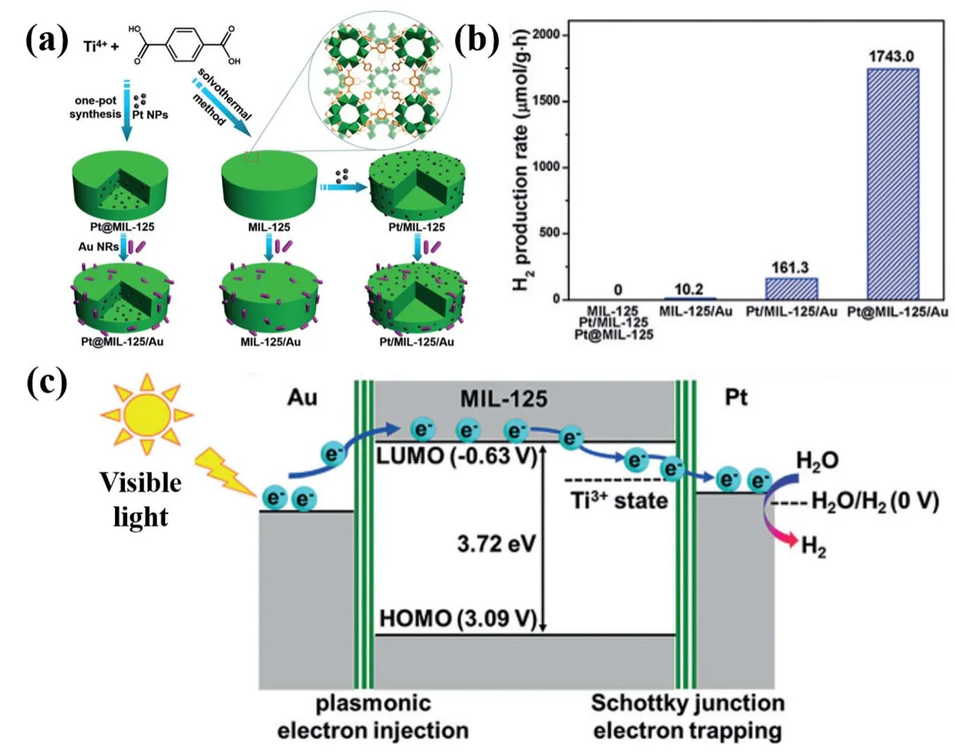
Fig. 16 (a) Schematic showing the synthesis of Pt@MIL-125/Au, Pt/MIL-125/Au and MIL-125/Au, (b) PHE of samples,(c)schematic based on energy levels showing electron migration at the metals/MOF interfaces

The electron-trapping ability of a cocatalyst is vital for H2production. With large work function and low Fermi level noble metals are excellent electron trappers. Among them, Pt is the largest in work function and is the most excellent for trapping electrons and has been extensively used as cocatalyst for photocatalytic hydrogen generation98. Pt nanoparticles can serve as electron sink as well as sites for effective proton reduction.Recently, Xiaoet al.49constructed a Pt@MOF/Au heterojunction photocatalyst. The Pt nanoparticles with size ofca.3 nm were uniformly dispersed into or supported on MIL-125 (Fig. 16). The Schottky junction between Pt and MIL-125 allows efficient transfer of hot electrons from Au nanorods to Pt nanoparticles through the MIL-125 material. Unlike MIL-125/Au and Pt/MIL-125, Pt@MIL-125/Au exhibited exponential enhancement of photocatalytic activity under visible light irradiation. Interestingly, the Pt nanoparticles inside MIL-125 showed much higher photocatalytic activity than those on the surface of MIL-125. This is attributed to the spatial separation of Pt and Au and the high specific surface area of MIL-125, which are beneficial for efficient transfer of hot electrons to the Pt nanoparticles to function as active sites for H2formation.
Due to the high price and limited supply of Pt, earthabundant materials have been extensively explored as cocatalysts to replace Pt93,95. Transition metal sulfides, MSx(M = Mo, Co,Ni), which are efficient in photocatalytic and electrocatalytic water splitting has been regarded as suitable alternatives99. Houet al. reported the construction of MoS2/g-C3N4layered heterojunctions through the delamination and reassembly of MoS2and g-C3N4100. With both MoS2and g-C3N4in layered structure, the geometric similarity allows minimization of lattice mismatch and facilitates the formation of planar MoS2/g-C3N4interfaces, leading to activity superior to that of Pt/g-C3N4(with Pt loading similar to that of MoS2). In addition, the intrinsic band structures of MoS2and g-C3N4enable directional migration of photogenerated electrons from g-C3N4to MoS2while keeping sufficient electrons for hydrogen reduction on MoS2. It is worth noting that the promotion mechanism of cocatalysts for PHE is controversial. The transfer path of photogenerated electrons and holes between semiconductors and cocatalysts, and the nature of active sites for hydrogen evolution should be studied in depth.
6 Summary and outlook
A large variety of semiconductor photocatalysts, including TiO2, WO3, MoS2, C3N4, CdS, Cu2O, have been studied for photocatalytic H2generation. Yet their activities remain far short of industrial requirements. The PHE process involves five steps:(i) reactant adsorption, (ii) light absorption, (iii) charge carrier separation and migration, (iv) surface redox reactions, and (v)product desorption. Great attention has been paid to the three that are directly related to photocatalysis,i.e., the light absorption to induce the generation of hot electrons and holes, charge separation and migration from bulk to the surface of semiconductor, and surface reactions for water splitting. Among them, light absorption ability is the first deciding factor and it is dictated by the band structure of photocatalysts. Various strategies have been applied to modify wide-band-gap semiconductors. As a type of anion defect, oxygen vacancies can effectively improve light absorption property by modulating the coordination structures and localized electrons of semiconductors. Metal nanoparticles exhibiting LSPR effect have been used to decorate the surface of semiconductors for the purpose of enhancing light trapping efficiency by means of light confinement and/or scattering. The second issue is the recombination of photoinduced electrons and holes that would result in loss of photocatalytic efficiency. Element doping for the tuning of electronic structure of photocatalysts is an effective way to promote charge transfer efficiency. Another prevalent method for guiding the separation of charge carriers is through the composition of two or three semiconductors to construct heterojunctions. Specifically, Z-scheme heterojunctions are simultaneously endowed with strong redox ability and spatially separated reductive and oxidative sites active for water splitting.Surface reaction is the final deciding factor for photocatalytic H2generation. Cocatalysts, such as Pt, MoS2, CoS2, and NiS, are deposited on photocatalysts with distinct positive effect on H2evolution activity. Nonetheless, the mechanism of the promotion effect on surface kinetics needs further investigation. It is important to mention that some of the strategies have more than one effect on the physiochemical properties of a photocatalyst.For example, the presence of oxygen vacancies not only extends light absorption, but also enhances charge separation and transport, and so does LSPR. Heterojucntion formation between two semiconductors not only increases the redox ability, but also improves light absorption due to the stacked configuration.Certain cocatalysts can not only accelerate the reaction but also suppress charge carrier recombination, but in some cases can hinder light penetration to the semiconductor. Thus it is critical to examine the possible effects for a particular strategy from all angles, no matter it is for rational design of a photocatalyst or for explaining a particular shift of performance. Furthermore, two or more of the mentioned strategies can be used in conjunction to boost photocatalytic performance for PHE, but careful design of the catalyst prior to experiment is highly recommended.
Despite great progresses have been made in the realm of photocatalytic evolution of H2in water splitting, there are challenges that demand future researches. First, the need of hole sacrificial agents in most reaction systems hinders industrialization owing to the extra cost. It is hence commendable to develop efficient and cheap photocatalysts and co-catalysts highly active for overall water splitting. On the other hand, although sacrificial agents are widely used, the effects of composition and concentration of sacrificial agents on PHE reaction are seldom studied and deserve investigation. Second,from an economic standpoint, the coupling of H2evolution with photocatalytic degradation of environmental pollutants or biomass reformation could be meaningful. Pollutants in wastewater, such as dyes, probiotics, pesticides, and many others, can act as hole scavengers and be oxidized and degraded to CO2or harmless intermediates. Semiconductor photocatalysts have the advantage of easy separation and good recyclability for the degradation process together with efficient production of H2.Third, most researches paid little attention to the processes of reactant adsorption and product desorption. The adsorption of water molecules and desorption of H2and O2molecules may have great influence on the overall PHE process. The chemical adsorption of the water molecules is essentially the activation of the reactant, which could lower the energy barrier and facilitate the reaction. Poor H2and O2desorption may result in blocking of active sites, and due to the buildup of gas layer hinder water adsorption while promoting the backward reaction of water formation. Unlike photoelectrochemical and electrochemical water splitting, where H2and O2are evolved in separate cell compartments, the separation of H2and O2in photocatalytic water splitting together with the suppression of backward reaction may become a sensible issue in the future. Furthermore,light propagation may also be affected by the scattering and reflection effect of the gas bubbles. Thus the design and preparation of photocatalysts that are hydrophilic and/or aerophobic in nature could be beneficial for photocatalytic H2production. The 3D structure of a photocatalyst and the presence of surfactants in the solution can also promote the detachment of bubbles. It is envisaged that this mini review can direct advanced researches for the design and development of state-of-the-art photocatalysts and open ways for effective solar energy conversion.