Resonant Tunneling of Holes Through δ-doped Be Acceptor GaAs/AlAs Multiple Quantum Wells
2019-11-19ZHENGWeiminHUANGHaibeiLISumeiCONGWeiyanWANGAifangLIBinSONGYingxin
ZHENG Wei-min, HUANG Hai-bei, LI Su-mei, CONG Wei-yan, WANG Ai-fang, LI Bin, SONG Ying-xin
(1. School of Space Science and Physics, Shandong University(Weihai), Weihai 264209, China;2. School of Chemistry and Chemical Engineering, Shandong University, Jinan 250100, China;3. School of Mechanical, Electrical & Information Engineering, Shandong University(Weihai), Weihai 264209, China;4. Shanghai Institute of Technical Physics, Chinese Academy of Sciences, Shanghai 200083, China;5. Jinan Semiconductor Research Institute, Jinan 250014, China)*Corresponding Authors, E-mail: wmzheng@sdu.edu.cn; binli@mail.sitp.ac.cn
Abstract: Three samples of GaAs/AlAs multiple quantum wells with different quantum-well widths are grown on semi-insulating (100) p-type GaAs substrates by the molecular beam epitaxy with Be acceptors δ-doped at the center of GaAs well layers. Three corresponding two-terminal devices are fabricated by photolithographic and semiconductor manufacturing technologies based on these samples. The device current-voltage characteristics are measured at temperatures in a range of 4-200 K. The resonant tunneling of heavy- and light-holes through Be δ-doped GaAs/AlAs multiple quantum wells are clearly observed. It is found that the position of resonant tunneling for light-heavy holes shifts to higher voltage with decreasing quantum-well sizes, which is in good agreement with the results calculated by the AlAs/GaAs/AlAs double-barrier theoretical model. However, as the measured temperatures increase, two peaks of resonant tunneling of light-holes move toward lower voltage, while one of the resonant peaks behaves as an oscillating mode at 150 K.
Key words: resonant tunneling; heavy- and light-holes; GaAs/AlAs multiple quantum wells; current-voltage characteristics; δ-doped
1 Introduction

In this paper, we report a study of resonant tunneling of the holes through GaAs/AlAs multiple quantum wells with Be acceptors δ-doped at the center of the GaAs well layers. Three samples for the GaAs/AlAs multiple quantum wells with different well size are grown by the molecular beam epitaxy on the GaAs substrate. Subsequently, three corresponding two-terminal devices are prepared in the clean room by semiconductor fabricated techniques for electronic micro-devices. TheI-Vcharacteristics of devices are measured at temperatures in a range of 4-200 K. The resonant tunneling of holes is investigated as a function of the quantum-well size and measured temperature. In addition, the transmission coefficient of the holes through Be δ-doped GaAs/AlAs multiple quantum wells is calculated by a double-barrier theoretical model.
2 Experimental Details and Theoretical Model
2.1 Experimental Details
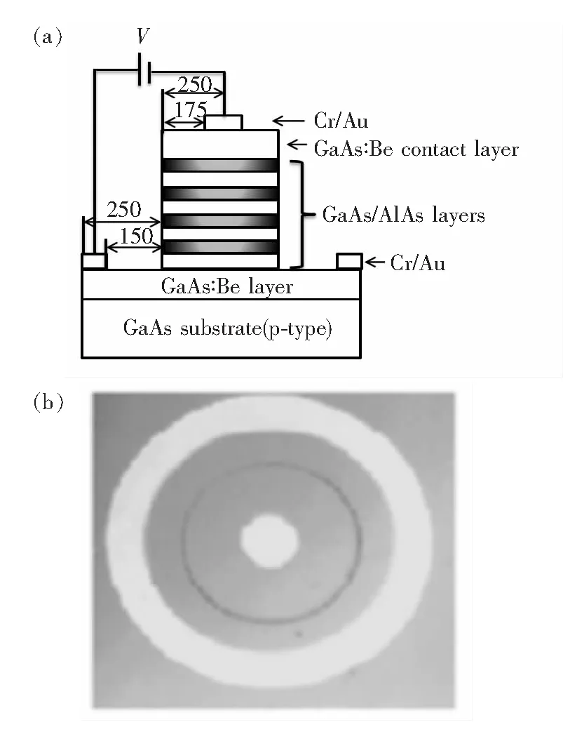
The samples used here were grown by the molecular beam epitaxy on semi-insulating (100) p-type GaAs substrates. Firstly, a GaAs buffer layer of thickness 300 nm, uniformly doped by Be acceptors of 2×1018cm-3, is grown on the substrate to provide a good crystallographic surface for succeeding quantum well layers. Above the buffer layer is GaAs/AlAs multiple quantum wells, which consist of a GaAs well layer with different widths and an identical 5 nm-wide AlAs barrier layer, while each of GaAs wells was δ-doped at the well center with Be acceptors. Subsequently, this multiple quantum-well layer is followed by a 200 nm GaAs contact layer of Be doping 2×1018cm-3. The growth of multiple quantum-well layers was controlled under the exact stoichiometric condition using the technique of low-temperature growth, which ensures high-quality optical materials even at relatively low temperatures. Under these conditions, the quantum-well samples were grown at 550 ℃ or 540 ℃ without interruptions at the quantum well interfaces, which ensured negligible diffusion of the Be δ-doped layers. The main features of each multiple quantum well structure are summarized in Tab.1.
Tab.1 Sample features of GaAs/AlAs multiple quantum wells: repeated periods, well width(Lw), Be δ-doped concentration(C) and growth temperature(T)

SamplesPeriodsLw/nm C/cm-2T/℃A140032×1010550A2200105×1010550A350152.5×1012540


2.2 Theoretical Model of Double Barriers
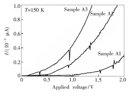
In Fig.2(a), the schematic diagram of valence-band is plotted for a GaAs quantum well sandwiched by AlAs double barriers under an applied bias. The interfaces between well and barrieris are labeled byI1,I2,I3, andI4, respectively, while the origin ofz-axis is placed at the interfaceI1of the left-hand barrier. Then forE ψ(z)=Aexp(ikz)+Bexp(-ikz)z ψ(z)=Mexp(κz)+Nexp(-κz)I1 (2) ψ(z)=Fexp(ikz)+Gexp(-ikz)I2 (3) ψ(z)=Hexp(κz)+Jexp(-κz)I3 (4) ψ(z)=Kexp(ikz)z>I4, (5) (6) with the boundary conditions at each interface used, theT(E) can be calculated by the transfer matrix method. Fig.2(b) shows theT(E) as a function of energy for the light holes incident on the AlAs(5 nm)/GaAs(L2nm)/AlAs(5 nm) quantum well structure with various well widthsL2. In the calculation ofT(E), the valence-band barrier height for the GaAs/Ga1-xAlxAs quantum well is taken asV(x)=0.33ΔEg(x), where ΔEg(x) is the energy difference of the band gaps atk=0 between GaAs and Ga1-xAlxAs bulk materials. ΔEg(x) is expressed as 1247xmeV, wherexis the mole fraction of the Ga1-xAlxAs material[19]. Furthermore, the light-hole effective mass is taken as 0.082m0which is the typical value of bulk GaAs, wherem0is the mass of electrons in the free space[20]. In Fig.2(b), several Dirac δ-functions can be seen at certain energies below the potential barrier heightV. At these resonance energies, the double-barrier GaAs/AlAs quantum well structure appears transparent and has a transmission coefficient of 1, which is known as a phenomenon of resonant tunneling. Assume that a hole moves from left to right in the applied electric field and impinges the left-hand AlAs potential barrier as shown in Fig.2(a), the resonant tunneling will occur only when the incident energy of the holes becomes approximately equal to that of the hole quantum states localized in the GaAs well. In addition, the resonance energies increase with decreasing quantum well widths, indicating the fact that the quantum well with a narrow well width has a stronger quantum-confined effect for holes, while the energy levels of holes shift to higher energy, compared to the one with a wide well size. Fig.2 (a) Schematic diagram of valence band for a AlAs/GaAs/AlAs quantum well structure under a bias. (b) Transmission coefficientT(E)versusenergy of light holes incident on a AlAs(5 nm)/GaAs(Lnm)/AlAs(5 nm) quantum well structure with the well width of 3, 10, 15 nm, respectively. Fig.3I-Vcurves for sample A1 at measured temperatures of 4, 50, 150, 200 K. As shown in Fig.4, theI-Vcharacteristicsversusbias are plotted at temperature 150 K for samples A1, A2 and A3 with the quantum-well sizes of 3, 10 and 15 nm, respectively. It can be seen that each ofI-Vcurves shows two resonant-tunneling peaks with different amplitudes and shapes. As the quantum well width is decreased, both resonant-tunnelling peaks shift to higher voltage with the amplitudes reduced, while the peak at higher voltage side evolves into an oscillatory behavior. As mentioned above, the two peaks are assigned to the resonant tunneling of light holes. This fact, that both of resonant peaks shift to higher voltage with decreasing the quantum-well width, is in good agreement with the computed results in Fig.2(b). The GaAs/AlAs multiple quantum-well system with a narrow well size has an even stronger quantum-confined effect for the holes in the GaAs well layer, compared to the one with a wide well size. The theoretic calculation of the subbands for heavy- and light-holes in the AlxGa1-xAs-GaAs quantum well structure indicates that the hole energy states move to higher energy as the well width decreases[14, 21-22]. Although the theoretical calculation in Fig.2(b) predicts three resonant-tunneling peaks of light holes for the double barriers GaAs/AlAs quantum-well structure with well widths of 10 nm and 15 nm, respectively, only two peaks are observed experimentally. This may be due to the band mixing and non-parabolicity effect for the heavy- and light-hole states. Another possibility is that the presence of the external electric field, especially at higher voltages, may modify the hole-subband structures. Fig.4I-Vcurvesversusapplied voltages at measured temperature 150 K for the sample A1, A2 and A3. We have investigated experimentally the resonant tunneling of holes through the Be δ-doped GaAs/AlAs multiple quantum well structures grown by the molecular beam epitaxy with the quantum-well widths of 3, 10,15 nm, respectively. Three corresponding two-terminal devices are fabricated in the super-clean room by semiconductor micro-device manufacturing techniques based on these different multiple quantum well structures. TheI-Vcharacteristics perpendicular to the layer plane for three devices are measured at the temperatures in a range of 4-200 K, respectively. The phenomena of resonant tunneling of light- and heavy-holes through the Be δ-doped GaAs/AlAs multiple quantum well system are observed clearly as a function of temperatures together with the quantum well sizes. It is found that the resonant-tunneling peaks of light-holes shift to higher voltages with decreasing quantum-well widths and measured temperatures, respectively, which is consistent with our theoretical model calculation.
3 Results and Discussion


4 Conclusion
