Optically controlled narrowband terahertzswitcher based on graphene
2018-04-19GREBENCHUKOVAlexanderZAITSEVAntonKHODZITSKYMikhail
GREBENCHUKOV Alexander N, ZAITSEV Anton D, KHODZITSKY Mikhail K
(ITMO University,Saint-Petersburg 197101,Russia)
1 Introduction
Currently, devices that can generate, control and receive the radiation in the terahertz(THz) frequency range have been widely researched and applied since the first sources and receivers of such radiation were created. THz radiation has nonionizing nature and easily passes through the majority of dielectrics, however it is strongly absorbed by conductors and some dielectrics. Due to the development of THz communications, the creation of devices to control THz radiation has huge importance[1]. The physical mechanisms allowing to modulate amplitude, phase or polarization of such radiation are researched. Controlling the properties of bulk materials(dielectric constant and conductivity) does not efficiently modulate the THz radiation.
Graphene is a two-dimensional allotropic modification of carbon with its atoms arranged in a hexagonal lattice. Graphene has many exceptional electrical, optical and mechanical properties such as the quantum Hall effect[2], the largest carrier mobility[3], variable optical conductivity[4], controllable plasmonic properties[5], high-speed operation and flexibility[6]. The frequency of graphene plasma waves lies in the terahertz(THz) frequency range[7], making graphene appealing for controllable terahertz devices, that can be tuned generally by an external electric field or optical pumping. The employing in-plane metamaterials in combination with a graphene allows controlling the properties of THz radiation efficiently.
In recent works, various hybrid structures based on graphene/metamaterial or graphene/waveguide were proposed. The effective optical properties are controlled by gate voltage[8-15], infrared optical pumping[16-17]or dual controlled(via optical illumination and gate voltage)[18]. The resonant frequency of such devices depends on the geometrical parameters of a unit cell and is close to the intrinsic metamaterial resonance. The main tunability mechanism is determined by the dynamic control of carrier concentration[9]in graphene by external influence. The majority of previous studies on tunable THz modulators are devoted to broadband modulation of THz radiation[8,11-19].
This work proposes and demonstrates for the first time the optically tunable narrowband THz switcher based on hybrid system consisting of graphene and metasurface with a cross-shaped elements. Such a structure provides polarization invariance. In this device, there is no need for gate electrodes and connecting wires, creation of which is a difficult technological problem. The geometrical parameters of the structure(size of the unit cell and cross-shaped elements) are selected according to the desired central resonant frequency of the device. In contrast to existing graphene-based relatively wide-band modulators the switcher offered in this work has a high-quality-factor transmission band. Moreover, it is activated after achieving a certain infrared(IR) pumping intensity and has high speed switching with the order of picoseconds[20]that allows using this device in wireless terahertz communications systems.
2 Conductivity model of graphene
Surface conductivityσ(ω) is often used to describe the optical properties of graphene, because its value can be measured over a wide frequency range[21]. It is known that surface conductivity of graphene is determined by two processes: interband and intraband transitions of carriers[22]. The gapless band structure of graphene leads to an unusual behavior of its conductivity. For visible and infrared ranges interband transitions dominate. In that frequency range surface conductivity is almost independent of the optical frequencyωand the chemical potentialμc(Fermi levelEf). For THz frequency range the intraband transitions[23]contribute greatly to the surface conductivity. In that frequency range there is a strong dependence of the surface conductivity with the Fermi level. Therefore, by changing the position of the Fermi level it is possible to control effectively the conductivity of graphene. This effect forms the basis of all tunable optoelectronic devices based on graphene.

(1)

(2)

(3)
whereiis an imaginary unit;kBis the Boltzmann constant;eis the charge of an electron; ћ=h/2π is the reduced Planck′s constant. As seen from the expressions (2) and (3) the surface conductivity is related to the environmental temperatureT; the relaxation timeτ=1 ps[25]; the optical frequencyωand the chemical potentialμc.
Under optical pumping of graphene with the light of visible and infrared range, photogeneration of electron-hole pairs occurs with an efficiency of 2.3%. Immediately after the optical pumping the electron-hole pairs tend to move into a state with lower energy. The optical generation of electron-hole pairs in graphene is described by the chemical potentialμc, where unexcited graphene is located at the intersection of the valence and conduction bands, and its energy is equal to zero. The value of the chemical potential under optical pumping is determined by[26]:
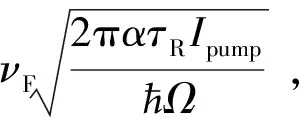
(4)
whereνFis the Fermi velocity(~106m/s);α=1/137 is the fine-structure constant[27];τR=1 ns is the characteristic recombination time[28];Ωis the frequency of pumping source corresponding to the wavelength ofλ=1 550 nm andIpumpis the intensity of a photo-doping pump source. The pumping source wavelength was chosen according to its prevalence in the communications.
The frequency dependent normalized conductivity of graphene depending on some selected values of the pumping intensity is shown in Fig.1(a) and 1(b). Fig.1(c) and 1(d) show the real and imaginary part of normalized surface conductivity of graphene as a function of the pump intensity and operation frequency.
The variation of the real and imaginary parts of the graphene surface conductivity causes changes of the amplitude and phase correspondingly of the electromagnetic(EM) wave propagating through the graphene monolayer. According to this fact, Fig.1(c) and 1(d) reveal that at low frequency there are significant losses and large possibilities of phase control of the EM wave, whereas at higher frequencies the reverse situation is observed. At this point high efficiency of graphene properties tuning can be achieved only by a compromise between low losses and sufficiently high phase changing. As seen from Fig.1, the largest difference between the imaginary parts of surface conductivity with and without pumping is observed at the frequency of 0.18 THz, but at the same frequency the significant value of the real part of surface conductivity is present. For this reason, the resonant frequency of the switcher developed was chosen in the higher frequency region of the spectrum where the losses are minimum and the difference between the value of Im(σ) is still significant with or without optical pumping. The frequencies near 0.4 THz satisfy this condition. In addition, there is a sufficient number of radiation sources, operating at frequencies close to 0.4 THz[29], that can be useful for the experimental verification of the calculations.
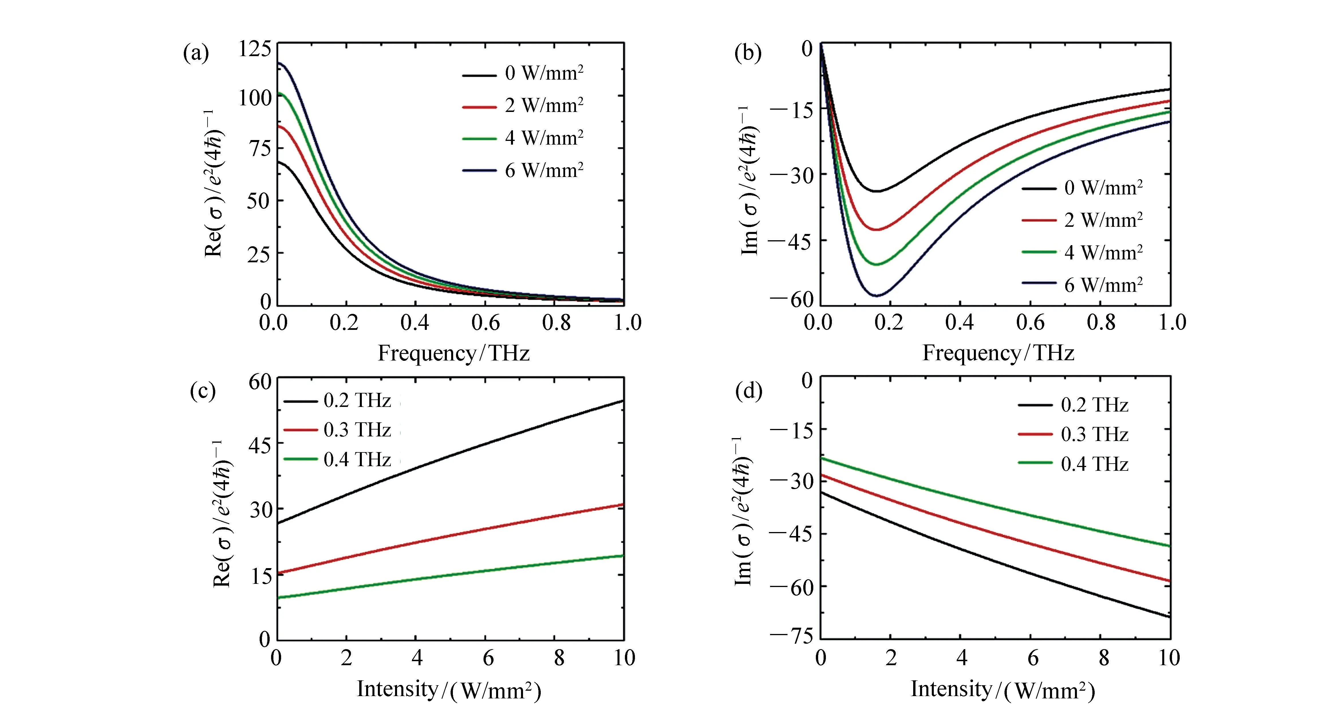
Fig.1 Spectrum of real(a) and imaginary(b) parts of normalized conductivity for single layer graphene at various pumping intensities. Real(c) and imaginary(d) parts of normalized conductivity as function of pumping intensity at various frequencies
3 Structural design and numerical modeling of switcher
The structure under consideration is shown in Fig.2. The unit cell of such a structure consists of graphene monolayer on the top of passive frequency selective surface(FSS), which is structured in the form of aluminum crosses with thickness of 0.5 μm. Graphene does not cover the walls of metal crosser. It is periodic in two directions (x) and (y) with periodicityG. The size of the crosses is in lengthLand in widthK, respectively. FSS with graphene is located on a dielectric polyethylene terephthalate(PET) substrate with the permittivity ofε=3 and thickness of 20 μm. PET is almost completely transparent in IR range, so a cooling system is unnecessary. The geometrical parameters of unit cell are set after performance optimization through EM simulation. The widthKand lengthLof each metal/graphene cross are 55.5 μm and 191.5 μm, respectively. The periodGof unit cell is 1 176 μm.

Fig.2 Schematic of the unit cell geometry under consideration: the periodic cross-shaped aluminum/graphene arrays with width K, length L and period G. The arrays are located on a PET substrate with thickness d. The incident EM wave is TE polarized with the electric fields along the y axis. The plane wave normally(along z) impinges on the switcher
The graphene was numerically modeled as a boundary condition characterized by a complex surface impedanceZ=1/σ, which is calculated based on Eqs. (1)-(4).
The use of analytical methods to describe all the effects occurring in such composite structure is difficult. Therefore, to solve the problem the numerical approach was applied. For all the simulations, the frequency domain solver of CST Microwave Studio, which solves Maxwell′s equations by means of the finite element method(FEM) was used. The frequency domain solver adopts with the unit-cell boundary conditions in thexandydirections and open Floquet ports in thezdirection. As a result of the simulation the S-parameters can be obtained. By using S-parameters obtained through the transmissionT(ω)=|S12|2, the reflectionR(ω)=|S11|2and the absorbanceA(ω)=1-T(ω)-R(ω) can be calculated.
4 Results and discussion
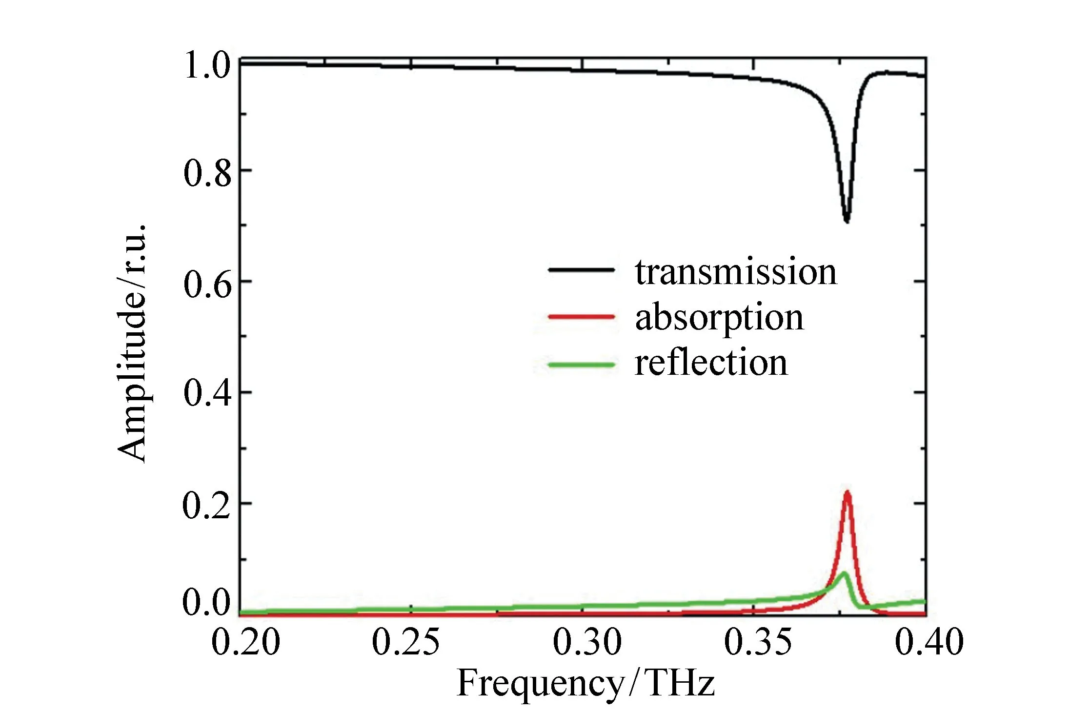
Fig.3 Transmission, reflection and absorption spectra of graphene based metamaterial switcher without optical pumping. The polarization of the incident light is along the y direction
First, the spectral characteristics of the graphene based metamaterial switcher without optical pumping have been investigated. Fig.3 illustrates calculated transmission, reflection and absorption spectra of such a structure with the intensity of optical pumping ofIpump=0 W/mm2. The results show that in the transmission curve of switcher a resonant dip is observed at 0.377 THz. At the same frequency there are maximum values of reflection and absorption. The dips in transmission spectra outcome mainly from the absorption.
Fig.4 plots calculate the transmission, reflection and absorption spectra of the graphene based metamaterial switcher under optical pumping with minimum threshold intensity ofIpump=0.2 W/mm2. Moreover, broad resonant dip(Q=60) in transmission at high frequency(0.377 THz), there is also high-Q(Q=250) resonant dip at low frequency(0.271 THz), which emerges at a certain value of optical pump intensity and does not shift with the increase of pump intensity up to 2 W/mm2, in contrast to the resonant dip at high frequency, which shifts to lower frequency. The modulation depth of transmission at 0.277 THz is 36.8%.
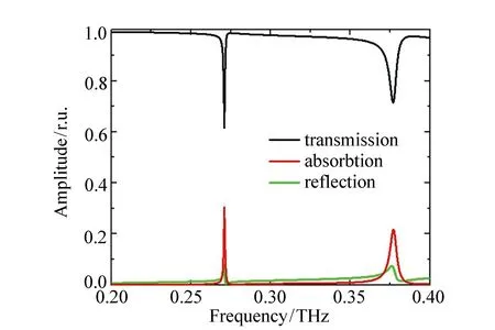
Fig.4 Transmission, reflection and absorption spectra of graphene based metamaterial switcher under optical pumping with intensity of Ipump=0.2 W/mm2. The polarization of the incident light is along the y direction
Such a behavior of dips is determined by their different nature[30]. The broad one stems from fundamental response of the frequency selective surface, and the resonance frequency depends on the size of crosses and effective index of surface plasmon polaritons(SPPs)[31]. At the same time the narrow one is associated with guided-mode resonances in the dielectric substrate and depends on the period and polarization angle[32]. Under optical pumping the effective index of SPPs is changed and causes a displacement of the resonant frequency of broad dip. Moreover, the optical pumping causes changes of electric field polarization, which determines the appearance of narrow dip in transmission spectrum. In addition, an increase of the pump intensity up to 2 W/mm2that enhances slightly the modulation depth in the transmission spectrum at frequency of emerged resonance dip is observed(see Fig.5). After 2 W/mm2, changes in the transmission level do not occur. The saturation in the absorption level of 32% is observed. The observed absorption level is lower than the one achieved earlier, but it is much higher in terms ofQ-factor[33-34].
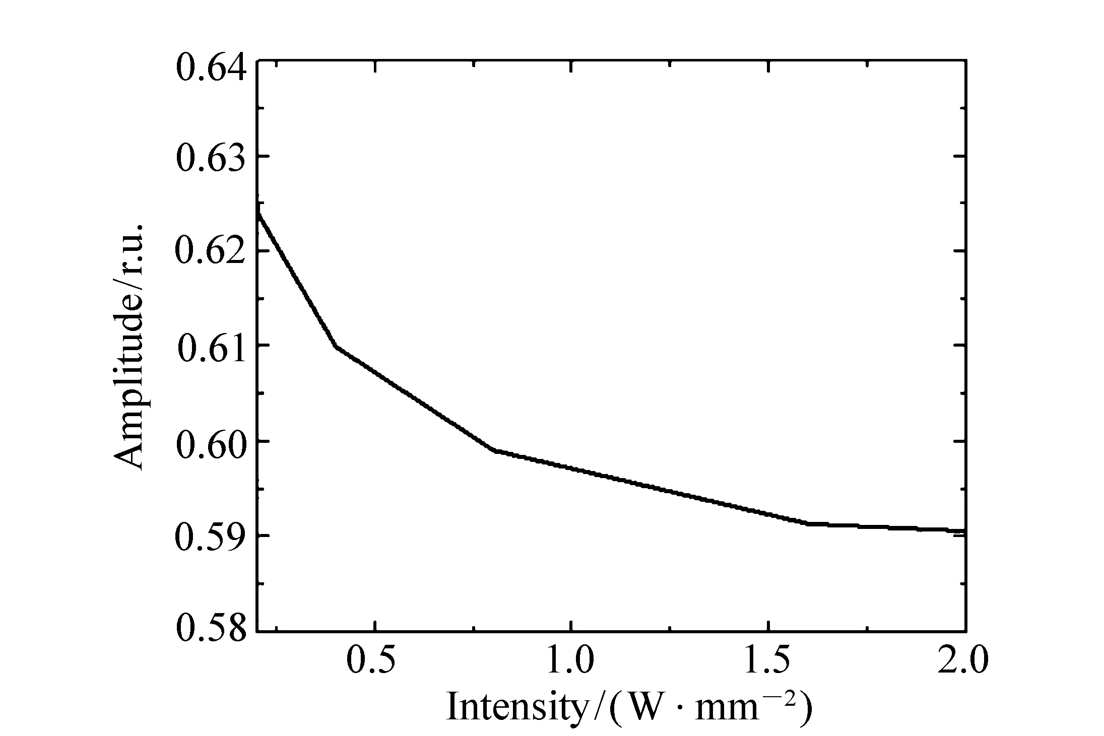
Fig.5 Transmission at 0.271 THz for different optical pumping intensity after turning on the switcher
In order to understand the mechanisms of resonance dip appearing in transmission spectrum, the electric field distribution of the graphene based metamaterial switcher at 0.271 THz, which corresponds with the resonant peaks shown in Fig.4 is calculated. The results for the case with and without optical pumping are shown in Fig.6.
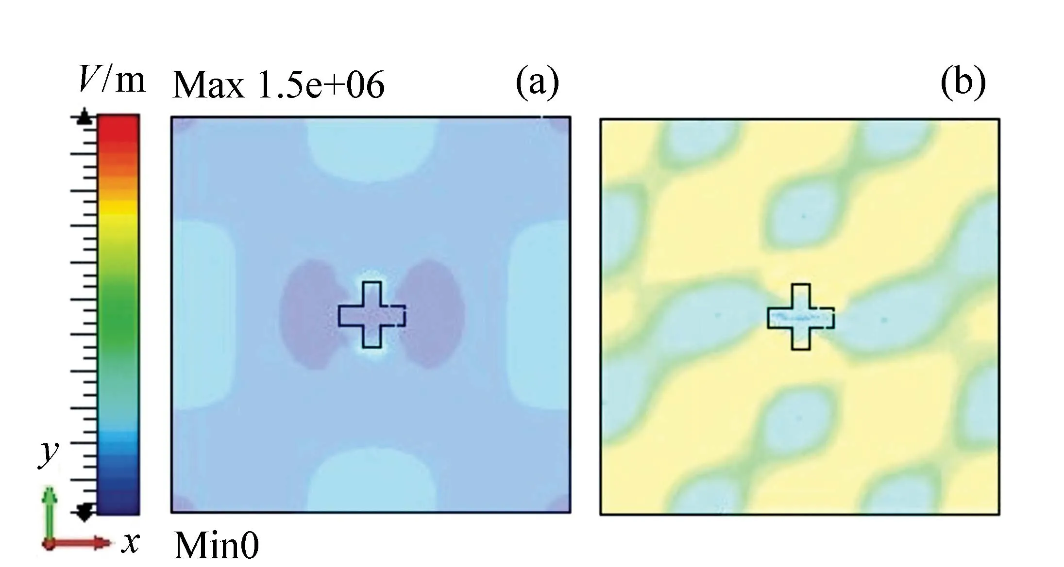
Fig.6 Electric field distributions from the metal surface of structure at the reflection and absorption peak(0.271 THz) without(a) and with(b) optical pumping(0.2 W/mm2)
The optical pumping of graphene causes the changes of polarization angle and excitation of guided-mode resonance, which is associated with the phased-matched first-order diffracted waves. Such a case is well illustrated in Fig.6. Moreover, after turning on the switcher the change of electric field polarization type is observed. Without the optical pumping in the area of a cross-shaped resonator there is an elliptical polarization. After switching by optical pumping the electric field polarization is changed to a linear type(see Fig.7). The size of arrows in Fig.7 displays the relative value of the electric energy density. This effect may be associated with the change of the diagonal elements of the effective permittivity tensor of the proposed composite structure.
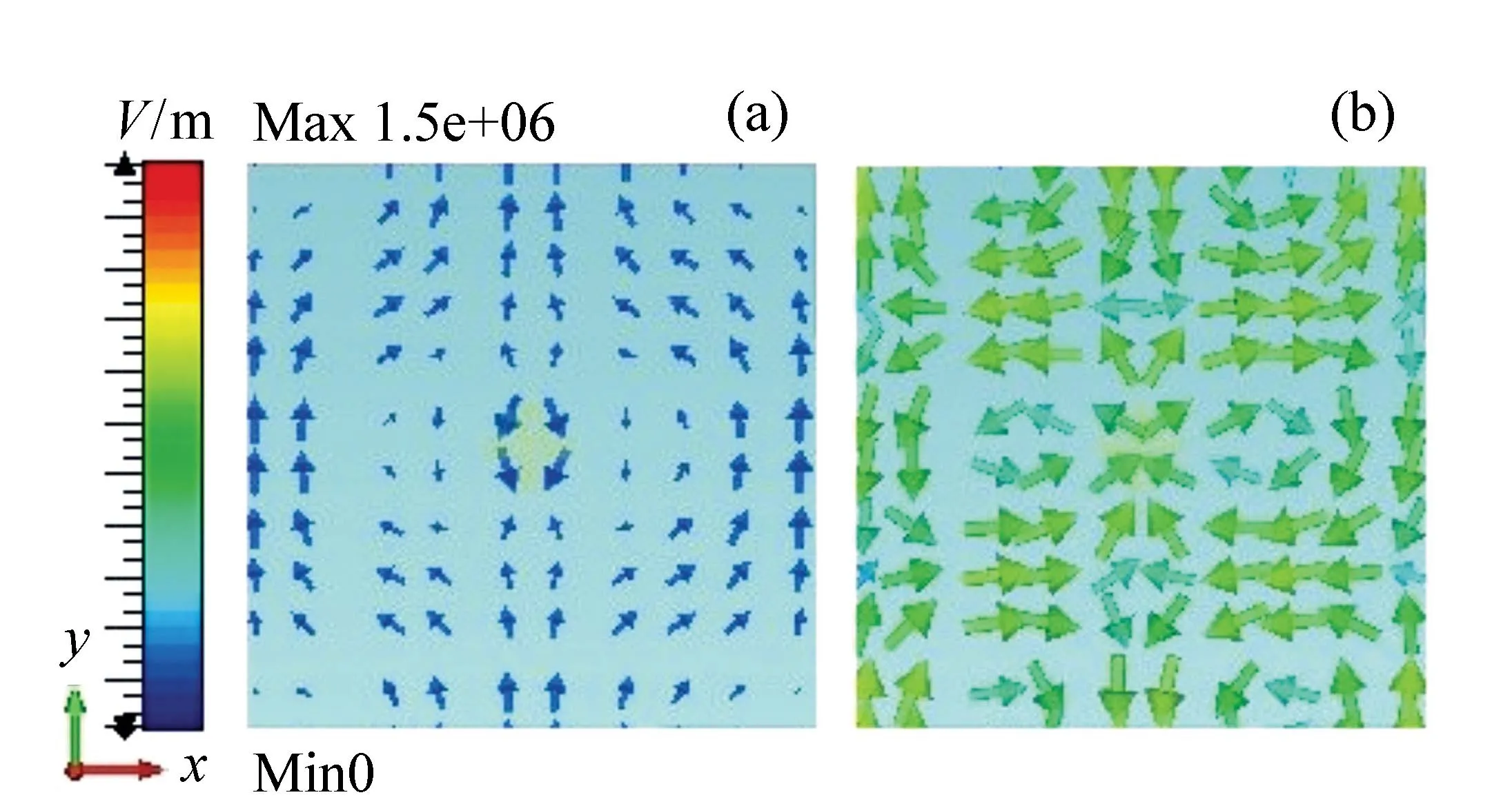
Fig.7 Distributions of electric field polarization from the metal surface at the reflection and absorption peak(0.271 THz) without(a) and with(b) optical pumping(0.2 W/mm2). The polarization of the incident light is along the y direction
5 Conclusion
In this paper, the design of optically controlled narrowband switcher based on graphene has been proposed and theoretically investigated by using the FEM. As a result of the investigation the spectral characteristics of THz switcher have been obtained. The composite structure proposed provides an ultrafast narrowband(Q=250) modulation switching at a certain threshold optical pumping intensity. The possibility to we amplitude to control THz wave passing through the switcher by changing the optical pump intensity without frequency shifting has been shown. Furthermore, the changing of electric field polarization type after turning on the switcher has been demonstrated.
[1]SONG H J,NAGATSUMA T. Present and future of terahertz communications[J].IEEETransactionsonTerahertzScienceandTechnology,2011,1:256-263.
[2]JIANG Z,ZHANG Y,TAN Y W,etal.. Graphene in extremely high magnetic fields[J].InternationalJournalofModernPhysicsB,2007,21:1123-1130.
[3]BOLOTIN K I,SIKES K J,JIANG Z,etal.. Ultrahigh electron mobility in suspended graphene[J].SolidStateCommunications,2008,146:351-355.
[4]BONACCORSO F,SUN Z,HAZAN T,etal.. Graphene photonics and optoelectronics[J].NaturePhotonics,2010,4:611-622.
[5]GRIGORENKO A N,POLINI M,NOVOSELOV K S. Graphene plasmonics[J].NaturePhotonics,2012,6:749-758.
[6]KIM K S,ZHAO Y,JANG H,etal.. Large-scale pattern growth of graphene films for stretchable transparent electrodes[J].Nature,2009,457:706-710.
[7]RANA F. Graphene terahertz plasmon oscillators[J].IEEETransactionsonNanotechnology,2008,7:91-99.
[8]HE X J,LI T Y,WANG L,etal.. Electrically tunable terahertz wave modulator based on complementary metamaterial and graphene[J].JournalofAppliedPhysics,2014,115:17B903.
[9]YANG K,LIU S,AREZOOMANDAN S,etal.. Graphene-based tunable metamaterial terahertz filters[J].AppliedPhysicsLetters,2014,105:093105.
[10]GAO W,SHU J,REICHEL K,etal.. High-contrast terahertz wave modulation by gated graphene enhanced by extraordinary transmission through ring apertures[J].NanoLetters,2014,14:1242-1248.
[11]LIN Y S,QIAN Y,MA F,etal.. Development of stress-induced curved actuators for a tunable THz filter based on double split-ring resonators[J].AppliedPhysicsLetters,2013,102:111908.
[12]LEE S H,CHOI M,KIM T T,etal.. Switching terahertz waves with gate-controlled active graphene metamaterials[J].NatureMaterials,2012,11:936-941.
[13]KAKENOV N,BALCI O,POLAT E O,etal.. Broadband terahertz modulators using self-gated graphene capacitors[J].JOSAB,2015,32:1861-1866.
[14]LIANG G,HU X,YU X,etal.. Integrated terahertz graphene modulator with 100% modulation depth[J].ACSPhotonics,2015,2:1559-1566.
[15]LAO J,TAO J,WANG Q J,etal.. Tunable graphene-based plasmonic waveguides: nanomodulators and nano attenuators[J].LaserPhotonicsRev.,2014,8:569-574.
[16]WEIS P,GARCIA-POMAR J L,HOH M,etal.. Spectrally wide-band terahertz wave modulator based on optically tuned graphene[J].ACSNano,2012,6:9118-9124.
[17]WEIS P,GARCIA-POMAR J L,RAHM M. Towards loss compensated and lasing terahertz metamaterials based on optically pumped graphene[J].OpticsExpress,2014,22:8473-8489.
[18]LI Q,TIAN Z,ZHANG X,etal.. Dual control of active graphene silicon hybrid metamaterial devices[J].Carbon,2015,90:146-153.
[19]CHEN X Y,TIAN Z. Recent progress in terahertz dynamic modulation based on graphene[J].ChineseOptics,2017,10:86-97.(in Chinese)
[20]LUO S,WANG Y,TONG X,etal.. Graphene-based optical modulators[J].NanoscaleResearchLetters,2015,10:199.
[21]REN L,ZHANG Q,YAO J,etal.. Terahertz and infrared spectroscopy of gated large-area graphene[J].NanoLetters,2012,12:3711-3715.
[22]HANSON G W. Dyadic Greens functions and guided surface waves on graphene[J].JournalofAppliedPhysics,2006,103:064302.
[23]WINNERL S,ORLITA M,PLOCHOCKA P,etal.. Carrier relaxation in epitaxial graphene photoexcited near the Dirac point[J].PhysicalReviewLetters,2011,107:237401.
[24]FALKOVSKY L A. Optical properties of graphene[J].JournalofPhysics:ConferenceSeries,2008,129:012004.
[25]DAWLATY J M,SHIVARAMAN S,CHANDRASHEKHAR M,etal.. Measurement of ultrafast carrier dynamics in epitaxial graphene[J].AppliedPhysicsLetters,2008,92:042116.
[26]RYZHII V,RYZHII M,OTSUJI T. Negative dynamic conductivity of graphene with optical pumping[J].JournalofAppliedPhysics,2007,101:083114.
[27]MAK K F,SFEIR M Y,WU Y,etal.. Measurement of the optical conductivity of graphene[J].PhysicalReviewLetters,2008,101:196405.
[28]RANA F,GEORGE P A,STRAIT J H,etal.. Carrier recombination and generation rates for intravalley and intervalley phonon scattering in graphene[J].PhysicalReviewB,2009,79:115447.
[29]LEWIS R A. A review of terahertz sources[J].Appl.Phys.D,2014,47:374001.
[30]FERRARO A,ZOGRAFOPOULOS D C,CAPUTO R,etal.. Broadand narrow-line terahertz filtering in frequency-selective surfaces patterned on thin low-loss polymer substrates[J].IEEEJournalofSelectedTopicsinQuantumElectronics,2017,23:1-8.
[31]KE S,WANG B,HUANG H,etal.. Plasmonic absorption enhancement in periodic cross-shaped graphene arrays[J].OpticsExpress,2015,23:8888-8900.
[32]FERRARO A,ZOGRAFOPOULOS D C,CAPUTO R,etal.. Angle resolved and polarization-dependent investigation of cross-shaped frequency selective surface terahertz filters[J].AppliedPhysicsLetters,2017,11:0141107.
[33]ANDRYIEUSKI A,LAVRINENKO A V. Graphene metamaterials based tunable terahertz absorber: effective surface conductivity approach[J].OpticsExpress,2013,7:9144-9155.
[34]HE X,ZHONG X,LIN F,etal.. Investigation of graphene assisted tunable terahertz metamaterials absorber[J].OpticalMaterialsExpress,2016,6:331-342.
Authorbiographies:
GREBENCHUKOV Alexander(1990—), PhD student, Department of Photonics and Optical Information Technology, ITMO University, Russia. His research interests focus on graphene-based tunable terahertz metamaterials and designing structures for superresolution. E-mail:grebenchukov_a@mail.ru
ZAITSEV Anton(1995—), Undergraduate student, Department of Photonics and Optical Information Technology, ITMO University, Russia. His research interests focus on graphene-based tunable terahertz metamaterials. E-mail:anleza@ya.ru
KHODZITSKY Mikhail(1984—), Chief of Terahertz Biomedicine Laboratory, Associate professor, Department of Photonics and Optical Information Technology, ITMO University, Russia. His research interests focus on terahertz photonics, metamaterials, biophotonics and terahertz spectroscopy. E-mail:khodzitskiy@yandex.ru
