Performance enhancement of CMOS terahertz detector by drain current∗
2017-08-30XingxingZhang张行行XiaoliJi纪小丽YimingLiao廖轶明JingyuPeng彭静宇ChenxinZhu朱晨昕andFengYan闫锋
Xingxing Zhang(张行行),Xiaoli Ji(纪小丽),Yiming Liao(廖轶明), Jingyu Peng(彭静宇),Chenxin Zhu(朱晨昕),and Feng Yan(闫锋)
College of Electronic Science and Engineering,Nanjing University,Nanjing 210093,China
Performance enhancement of CMOS terahertz detector by drain current∗
Xingxing Zhang(张行行),Xiaoli Ji(纪小丽)†,Yiming Liao(廖轶明), Jingyu Peng(彭静宇),Chenxin Zhu(朱晨昕),and Feng Yan(闫锋)
College of Electronic Science and Engineering,Nanjing University,Nanjing 210093,China
In this paper,we study the effect of the drain current on terahertz detection for Si metal-oxide semiconductor field effect transistors(MOSFETs)both theoretically and experimentally.The analytical model,which is based on the small signal equivalent circuit of MOSFETs,predicts the significant improvement of the voltage responsivity Rvwith the bias current.The experiment on antennas integrated with MOSFETs agrees with the analytical model,but the Rvimprovement is accompanied first by a decrease,then an increase of the low-noise equivalent power(NEP)with the applied current.We determine the trade off between the low-NEP and high-Rvfor the current-biased detectors.As the best-case scenario,we obtained an improvement of about six times in Rvwithout the cost of a higher NEP.We conclude that the current supply scheme can provide high-quality signal amplification in practical CMOS terahertz detection.
drain current,CMOS terahertz detectors,voltage responsivity,noise equivalent power
1.Introduction
Recently,there has been a large increase of practical interest in metal-oxide semiconductor field-effect transistor (MOSFET)-based terahertz detectors owing to their advantages,including their low cost,low power consumption,wide spectral response,and their high compatibility with CMOS logic circuits.Further,there has been a significant focus on the research and development of high-performance terahertz detectors that are fabricated by various advanced CMOS technologies.Sherry et al.[1]used a more advanced 65-nm silicon-on-insulator(SOI)process technology.Sengupta et al.[2]used the modified circuit concepts in combination with a cost-efficient 0.13-µm CMOS technology and the silicon germanium-based BiCMOS technology.In addition,more researchers have used the thinned substrate technology.[3–5]Although these fabricated chips have a high-Rvand low-NEP compared to those obtained by standard technologies,the fabrications clearly require dedicated facilities as well as more advanced process technologies,which inevitably increase the product cost and manufacturing complexities.Instead of the advanced technologies,recent developments pertaining to CMOS terahertz detectors have demonstrated that the asymmetric FET structures have the potential to dramatically improve the detector performance.These asymmetric structures include the asymmetry when feeding the incoming radiation with a special antenna,[6]the asymmetry between the source and drain structures,[7]and the asymmetry boundary conditions that are due to a current biased to the channel of the devices.[8–12]In the latter case,the external field that induced the electron concentration and potential near the drain side change dramatically,resulting in the device being more sensitive to the external perturbations.However,it should also be noted out that the impressive improvement obtained with the applied current is accompanied by an increase of the detection noise,which limits the applicability of the current-biasing scheme to applications.
In this work,we present an analytical model for current biased terahertz detectors based on the small-signal equivalent circuit of MOSFETs.Then,we study the Rvand NEP under the current bias condition using antenna-integrated Si MOSFET detectors.Furthermore,we designed a current–mode circuit integrated with the detectors to provide the signal amplification inside the pixel.
2.Small-signal equivalent circuit-based model
We can use sub-micro MOSFETs for terahertz detection as nonlinear properties of plasma wave excitations in FET channels enable their response at frequencies that are appreciably higher than the device cutoff frequency.[13–17]The basic mechanism and operating mode of CMOS terahertz detectors have been described in detail in many studies.When terahertz signals are coupled to the gate terminals of MOSFETs,the transistors under the modified gate voltage rectify the signals,generating a DC source–drain voltage,and they can be detected.

Fig.1.(color online)Schematic diagram of MOSFETs operating in the terahertz detection mode.
To illustrate the effect of the current bias on the detector response,we first utilize an analytical model to extract Rvand NEP of the current-biased MOSFET detector based on the small-signal equivalent circuit.Figure 1 shows the schematic geometry of MOSFETs used for terahertz detection;here,the drain current Idsis provided by a power supply Vdcconnected with a resistor R.When the terahertz radiation vRF=VRFsinωt is imported from the source side of the channel,the transistors under the modified gate voltage rectify the signal and generate a dc current and voltage at the drain side as follows:
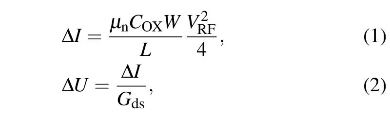
where Gdsis the channel’s conductance,which can be readily adjusted by controlling the drain current in the strong inversion condition.By defining FET operation conditions by the values of Vgs,Vds,and Ids,we can then calculate Gdsas

Substituting Eqs.(1)and(3)into Eq.(2),we can then describe an analytic expression for the rectified voltage ΔU, including the current bias,as

The equation links the current-induced enhancement of the rectified signal with the ratio of Ids/Ids,sat,and predicts that the voltage response ΔU of the MOSFET detector sharply increases when the applied current Idsapproaches the saturation current Ids,satfor a given gate voltage.The small-signal analysis of the current-mode provides equations in a similar way to the one developed using the hydrodynamic equation described in Ref.[8].For the zero-current situation in the strong inversion condition,equation(6)reducesto the well-known relation

The Rvof the current-biased MOSFET detector can be calculated from Eq.(6)as

where Rinis the real part of the input impedance of the detector.
When we consider only the thermal noise in the circuit, NEP of the detectors in the voltage read-out circuit can be written as follows:

where SV,Rchand SV,Rrepresent the fluctuations in the thermal noise-voltage fluctuation spectral density induced by the channel resistance and the additional resistor R,respectively.
3.Experimental and results
We fabricated the MOSFET detectors studied here using 0.18-µm standard CMOS technology integrated with a 650-GHz patch antenna with an area Sdetof 1.1×104µm2. The gate length and width of the MOSFETs are 0.18µm and 0.5µm,respectively,and the threshold voltage Vthis 0.5 V.We obtained a terahertz source with a wavelength ranging from 610–680 GHz using an Agilent E8257D signal generator and VDI AMC-T136 frequency multiplier.We measured the ΔU of the devices using the standard lock-in technique,and we measured the noise-voltage fluctuation spectral density of the detector using an Agilent 35670a signal analyzer.Additional components such as integrated amplifiers are not included in the measurement to avoid the excess noise,which makes the study of the pure MOSFET devices with regards to the NEP more difficult.
According to Eq.(8),we can calculate Rvusing ΔU and the incident power Pinon the detector.To obtain Pin,we first calibrated the space distribution of the incident power density, and the radiation power received by the antenna is then calculated as:

where Pdis the power density on the detector position and Sdetrepresents the antenna area in the detector.
Figure 2 shows the Rvof the detector with the current bias for gate voltages ranging from 0.40 V to 0.53 V.We see that Rvfor a given gate voltage first increases significantly with the current,after which it saturates and reaches a maximum voltage responsivity Rv,max,which is marked by the arrow in the figure.The solid curve in Fig.2 is related to the calculated responsivity using Eq.(6)for the gate bias Vgs=0.49 V.The calculated curve agrees well with the experimental data in the sub-threshold and linear regions of the transistors.However, the deviation between the theoretical calculation and the measured values at the large Idsis significant.There was a previous report of a similar phenomenon in InGaAs/GaAs HEMT detectors,where the deviation is considered to be due to the current saturation of the transistors.[18]To understand the reason for this,we extracted the gate-bias dependence of the saturation current from the Rvof the detector,Rv−Idscurves, and from the Ids−Vdscharacteristics of MOSFETs.The results are shown in Fig.3.We observe that two datasets exhibit good agreement,confirming the relationship between the responsivity saturation and the drain-current saturation.Under the condition of saturation currents,the electric field near the drain remains finite with drain currents,leading to the stable channel’s conductance and the responsivity saturation.

Fig.2.(color online)Bias-current dependence of R v for CMOS detector under 680-GHz radiation with a 1 kHz electronic chopper.The solid line represents the theoretical calculation using Eq.(6)for the gate bias V gs=0.49 V.The arrow in the figure shows the value of the current that corresponds to the saturated R v.
Figure 4 shows the current bias dependence of the Rv,maxunder the various gate biases.For the range of the relatively low bias current,Rv,maxfollows a linear dependence with the current as follows:
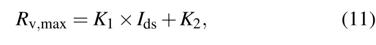
where K1and K2are 4.3 kV/(W·µA)and 2.4 kV/W,respectively.Using the equation,we can predict the possible Rvenhancement of detectors for a given current.

Fig.3.Saturation drain current versus the gate bias obtained using two different methods.The hollow circle data are extracted from the R v–I ds curve in Fig.2,while the solid circle data are extracted from I ds–V ds characteristics of MOSFETs,as shown in the inset of the figure.

Fig.4.(color online)Bias-current dependence of R v,max.The dashed line is the linear fitting curve.

Fig.5.(color online)Measured S V of detectors under the condition for R v,max.The dashed lines represent the fitting obtained using the noise model,considering the thermal noise and G−r noise source.
Next,we focus on the noise characteristics of the device. Figure 5 shows the measured voltage-fluctuation spectral density SVof detectors under the various currents.The spectra exhibit frequency dependence,and the bias current enhances the noise level of the detectors.The high-frequency roll-off behavior above 104Hz,which we observed even in the zerocurrent bias condition,is considered from the loading of the device with an external RC circuit.On the other hand,on the low-frequency side,the noise in the MOSFETs is usually modeled by the thermal noise from the channel resistance.We evaluated the thermal noise spectral density SV,Tfor the detectors.The results are listed in Table 1,and show that the estimated values obtained from the thermal noise are much smaller than the ones observed in Fig.5,indicating that other noise sources may be involved besides the thermal noise.

Table 1.Main parameters used in S V−f fitting.
The G−r noise is one important fluctuation within the range of the low frequencies owing to trapping and de-trapping processes between the carriers and deep-level traps in the oxide layer near the Si/SiO2interface of MOSFETs.When we considered the G−r noise mechanism,the total noise spectral density can be expressed as

Here,SV,G−ris expressed as[19]
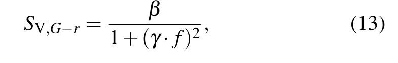
with
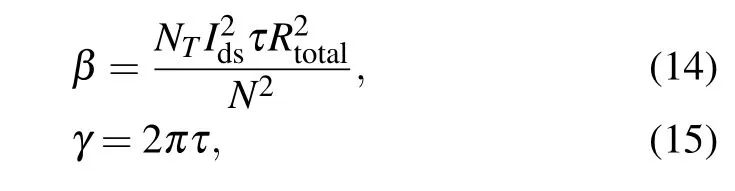
where N and NTare the total number of free carriers and traps, respectively,and τ is the capture and emission time constant of the carriers.
The proposed model demonstrates a close fit to the experimental frequency characteristic of SV,as shown in Fig.5.The parameter values used in the fitting are listed in Table 1.Values such as the intrinsic carrier concentration and trap concentration are obtained from standard MOSFET values.Table 1 also shows the SVconstituents under three fixed currentvalues. We observe that SV,G−rprevails in the measured frequency region when the current flows in the detectors.At the current of 0.6µA,the G−r noise is about one order of magnitude greater than the thermal noise.The increase in the bias current enhances the G−r noise dramatically,from 2.3×10⁻¹⁴V2/Hz at 0.6µA to 1.8×10⁻¹²V2/Hz at 3.7µA,while the thermal noise component shows a relatively weak current dependence. The significant enhancement of the G−r noise may be due to the larger trapping and de-trapping time constants as well as the channel resistance under the higher currents.
Figure 6 shows the bias current dependence of the NEP that was evaluated from the experimental data of Rv,maxand SVat a frequency of 1 kHz.We observe that the magnitude of NEP first decreases and then increases with the applied current.As shown as the black dot in Fig.6,the detector with an applied current of 2.3µA has the same NEP value as that of the unbiased detector.We then determined the trade off between low-NEP and high-Rvfor the current-biased detectors by comparing the data of NEP and Rvin Fig.4.We found that the performance of CMOS terahertz detectors could be improved by introducing small drain currents below 2.3µA. In the best-case scenario,we can obtain an improvement by a factor of six in Rvwithout the need for a more costly NEP. The results reveal that even though there is a relative increase in the voltage noise with the current bias,we may register an unambiguous current-bias condition to provide a high-quality signal amplification for CMOS terahertz detectors.

Fig.6.(color online)Bias-current dependence of NEP evaluated from the experimental data of R v,max and S V for a modulation frequency of 1 kHz.The black dot shows that the detector with the applied current of 2.3µA has the same NEP value as that of the unbiased detector.
For MOSFETs,terahertz detection can be self-amplified using the drain current.However,the present current supply scheme using a dc power source with a resistor is not a suitable solution for large-array integrated circuits(ICs).For an increased integration and sensitivity of the CMOS detectors,we then propose an on-chip circuit with the current mirror structure for current-biased CMOS terahertz detectors.
Figure 7 shows the current supplying circuit,which consists of a sub-circuit with a current source(M1–M4)and antenna-coupled FET pairs(M5,M6)in differential operation.In the current-source circuit,the cascode current mirror is the core structure,and can increase the output resistance of a current source and suppress the effect of channel-length modulation on the accuracy of the applied current Ids.The cascode structure can shield the transistor M3 from the variations that are due to the detection circuits,and the voltage bias Vds3is equal to Vds1with high accuracy.[20]By designing suitable-sized MOSFETs,the relationship between Idsand the reference IREF,as shown in Fig.7,can then be written as

The equation indicates that a reference current IREFcan provide multiple detectors with stable current Idsfor array detectors.A CMOS terahertz detector that is integrated with such a current-supply circuit is more conductive to those applications.
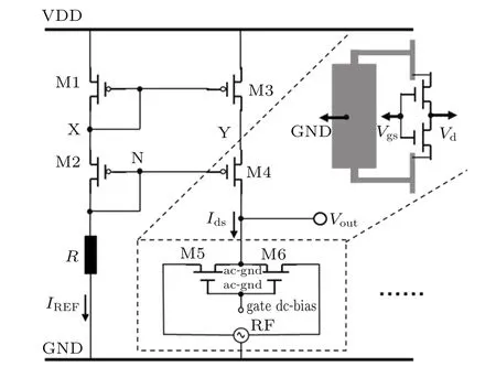
Fig.7.Schematic diagram applied for CMOS terahertz detectors operating in the current mode.The dashed square indicates the lowfrequency equivalent circuit of an antenna-coupled CMOS detector with its high-frequency one presented in the zoomed-up area.
4.Conclusions
We studied the influence of the drain-to-source current on the performance of CMOS terahertz detectors.The analytical model based on the small-signal equivalent circuit of MOSFETs predicts the improvement in the Rvof MOSFET detectors with the bias current.We performed an experiment using antennas integrated with MOSFETs,and the results agree with the analytical model,but the improvement in the Rvthat is obtained using the applied current is accompanied first by a decrease,then an increase in NEP.We find that there is a marked improvement beyond the Rvand NEP values of the unbiased device.Further,we designed the current-supply circuit integrated with the detector for practical devices.
[1]Sherry H,Hadi R A,Grzyb J,Öjefors E,Cathelin A,Kaiser A and Pfeiffer U R 2011 Radio Frequency Integrated Circuits Symposium (RFIC)1–4
[2]Sengupta K,Seo D,Yang Land Hajimiri A 2015 IEEE Trans.Terahertz Sci.Tech.5 427
[3]Schuster F,Coquillat D,Videlier H,Sakowicz M,Teppe F,Dussopt L, Giffard B,Skotnicki T and Knap W 2011 Optics Express 19 7827
[4]Hadi R A,Sherry H,Grzyb J,Zhao Y,Forster W,Keller H,Cathelin A, Kaiser A and Pfeiffer U R 2012 IEEE Journal of Solid-State Circuits 47 2999
[5]Schuster F,Videlier H,Dupret A,Coquillat D,Sakowicz M,Rostaing J,Tchagaspanian M,Giffard B and Knap W 2011 IEEE International Solid-State Circuits Conference 42
[6]Lisauskas A,Pfeiffer U,Öjefors E,Bolivar P H,Glaab D and Roskos H G 2009 J.Appl.Phys.105 114511
[7]Ryu M W,Lee J S,Park K,Kim K R,Park W K and Han S T 2013 Simulation of Semiconductor Processes and Devices(SISPAD)200
[8]Dyakonov M and Shur M 1993 Phys.Rev.Lett.71 2465
[9]Tombet S B,Tanimoto Y,Satou A,Suemitsu T,Wang Y,Minamide H, Ito H,Fateev D V,Popov V and Otsuji T 2014 Appl.Phys.Lett.104 262104
[10]Lisauskas A,Boppel S,Matukas J,Palenskis V,Minkevičius L,Valušis G,Bolívar P H and Roskos H G 2013 Appl.Phys.Lett.102 153505
[11]Veksler D,Teppe F,Dmitriev A P,Kachorovskii V Y,Knap W and Shur M S 2006 Phys.Rev.B 73 125328
[12]Lu J Q and Shur M S 2001 Appl.Phys.Lett.78 2587
[13]Fatimy A E,Teppe F,Dyakonova N,Knap W,Seliuta D,Valusis G, Shchepetov A,Roelens Y,Bollaert S,Cappy A and Rumyantsev S 2006 Appl.Phys.Lett.89 131926
[14]Knap W,Deng Y,Rumyantsev S,Lu J Q,Shur M S,Saylor C A and Brunel L C 2002 Appl.Phys.Lett.80 3433
[15]Knap W,Kachorowskii V,Deng Y,Rumyantsev S,Lu J Q,Gaska R, Shur M S,Simin G,Hu X and Khan M A 2002 J.Appl.Phys.91 9346
[16]Meziani Y M,Lusakowski J,Dyakonova N,Knap W,Seliuta D,Sirmulis E,Deverson J,Valusis G,Boeuf F and Skotnicki T 2006 IEICE Trans.Electr.E89-C 993
[17]Dyer G C,Crossno J D,Aizin G R,Mikalopas J,Shaner E A,Wanke M C,Reno J L and Allen S J 2009 Proc.SPIE 721503
[18]Elkhatib T A,Kachorovskii V Y,Stillman W J,Rumyantsev S,Zhang X C and Shur M S 2011 Appl.Phys.Lett.98 243505
[19]Haartman M V andÖstling M 2007 Low-frequency Noise in Advanced MOS Devices(Springer Scienceamp;Business Media)pp.11–12
[20]Behzad R 2003 Design of Analog CMOS Integrated Circuits(Xi’an: Xi’an Jiaotong University Press)pp.116–121
17 April 2017;revised manuscript
7 June 2017;published online 31 July 2017)
10.1088/1674-1056/26/9/098401
∗Project supported by the National Key Ramp;D Program of China(Grant No.2016YFB-0402403),the Natural Science Foundation of Jiangsu Province, China(Grant No.BK20141321),CAST Project,China(Grant No.08201601),and the National Science Foundation for Young Scholars of China(Grant No.61404072).
†Corresponding author.E-mail:xji@nju.edu.cn
©2017 Chinese Physical Society and IOP Publishing Ltd http://iopscience.iop.org/cpb http://cpb.iphy.ac.cn
杂志排行

Chinese Physics B的其它文章
- Improved control for distributed parameter systems with time-dependent spatial domains utilizing mobile sensor actuator networks∗
- Geometry and thermodynamics of smeared Reissner–Nordström black holes in d-dimensional AdS spacetime
- Stochastic responses of tumor immune system with periodic treatment∗
- Invariants-based shortcuts for fast generating Greenberger-Horne-Zeilinger state among three superconducting qubits∗
- Cancelable remote quantum fingerprint templates protection scheme∗
- A high-fidelity memory scheme for quantum data buses∗