Inverted organic solar cells with solvothermal synthesized vanadium-doped TiO2 thin films as efficient electron transport layer
2017-08-30MehdiAhmadiSajjadRashidiDafehSamanehGhazanfarpourandMohammadKhanzadeh
Mehdi Ahmadi,Sajjad Rashidi Dafeh,Samaneh Ghazanfarpour,and Mohammad Khanzadeh
Department of Physics,Faculty of Science,Vali-e-Asr University of Rafsanjan,Rafsanjan,Iran
Inverted organic solar cells with solvothermal synthesized vanadium-doped TiO2thin films as efficient electron transport layer
Mehdi Ahmadi†,Sajjad Rashidi Dafeh,Samaneh Ghazanfarpour,and Mohammad Khanzadeh
Department of Physics,Faculty of Science,Vali-e-Asr University of Rafsanjan,Rafsanjan,Iran
We investigated the effects of using different thicknesses of pure and vanadium-doped thin films of TiO2as the electron transport layer in the inverted configuration of organic photovoltaic cells based on poly(3-hexylthiophene)P3HT: [6-6]phenyl-(6)butyric acid methyl ester(PCBM).1%vanadium-doped TiO2nanoparticles were synthesized via the solvothermal method.Crystalline structure,morphology,and optical properties of pure and vanadium-doped TiO2thinfilms were studied by different techniques such as x-ray diffraction,scanning electron microscopy,transmittance electron microscopy,and UV–visible transmission spectrum.The doctor blade method which is compatible with roll-2-roll printing was used for deposition of pure and vanadium-doped TiO2thin films with thicknesses of 30 nm and 60 nm.The final results revealed that the best thickness of TiO2thin films for our fabricated cells was 30 nm.The cell with vanadium-doped TiO2 thin film showed slightly higher power conversion efficiency and great Jscof 10.7 mA/cm2compared with its pure counterpart.In the cells using 60 nm pure and vanadium-doped TiO2layers,the cell using the doped layer showed much higher efficiency.It is remarkable that the external quantum efficiency of vanadium-doped TiO2thin film was better in all wavelengths.
inverted polymer solar cells,electron transport layer,vanadium-doped TiO2thin films,solvothermal
1.Introduction
In recent years,polymer solar cells(PSCs)gained a lot of attention because of their superior characteristics such as mechanical flexibility,low cost,low environmentalload,and their potential to be produced in large scale.[1–3]However,PSCs technology is not mature yet.PSCs,especially those with normal configuration,suffer from instability and low power conversion efficiency(PCE).[4]These photovoltaic cells have common problems in the PEDOTS:PSS layer.This layer is sensitive to ambient conditions and its acidic nature increases the degradation rate of the layer.Oxidation of low work function top metal oxide with the degradation of the PEDOT:PSS layer under UV illumination is another problem of the normal configuration of PSCs.[5–9]An inverted configuration is a common approach seeking to overcome the mentioned problems of PSCs.[3,9]In this structure,a bufferlayeris inserted between the active layers and electrodes.Different n-type metal oxides such as ZnO[9–12]and TiO2,[13–15]alkali metal oxides like LiF[16]and Cs2CO3,[17,18]and in some cases ultra thin layers of Ca[19,20]are used as the electron-selective and holeblocking layer in PSCs.
Special qualities of TiO2cause it to be widely used in semiconductor industries such as OLEDs and organic photovoltaic cells.The TiO2thin film has high electron mobility,great optical transparency,good physical and chemical stability;and as a nontoxic material,it can be produced in large scale inexpensively.Also,TiO2has substantial oxygen and water protection because of photocatalysis combination and inherent oxygen deficiency.[21–23]Atomic layer deposition,[14,23]magnetron sputtering,[13,24]doctor blade method,[25]and spin coating[26]are some of the techniques used to fabricate TiO2thin films.Some reports show that doping TiO2can improve the performance of solar cells.For example,a Cs-doped TiO2interlayer exhibited a power conversion efficiency of 4.2%,while pure thin films of TiO2showed PCE of∼2.4%.[9]Materials such as Al,Ga,and In were used as dopants in ZnO(ETLs)to enhance the electrical properties of the thin films and improve the PCE of cells.[27–30]Materials such as vanadium and niobium could be used as a dopant to improve the electrical properties of TiO2as an electron transport layer.Vanadium has a resonant level within the conduction band of Ti and it can be used as a promising dopant to create a high density of free carriers.[31–34]In this study,we investigate cells using 1%vanadium-doped TiO2thin films with different thicknesses and compare them with those using pure TiO2thin films.
2.Experiment
All chemicals were used as received without further purification.Titanium(IV)butoxide(TB,97%),oleic acid (OA,90%),and oleylamine(OM,70%)were purchased from Sigma-Aldrich.Absolute ethanol(anhydrous,ACS,94%–96%)and vanadium(V)oxytriethoxide(VO(OPr)3,95%) were also purchased from Sigma-Aldrich.In this work,pure and vanadium-doped TiO2nanoparticles(NPs)were prepared by the solvothermal method.[31]Typically,TB(2.27 ml, 6.7 mmol)and VO(OPr)3(0.018 g,1%V/Ti mole ratio)were added to a mixture of 10.57 ml(33.3 mmol)OA,10.97 ml (33.3 mmol)OM,5.84 ml(100 mmol)absolute ethanol,and 0.67 ml(36.7 mmol)deionized(DI)water.The obtained mixture was stirred under argon atmosphere for 10 min before being transferred into a 50 mL Teflon-lined stainless steel autoclave.The system was then heated at 180°C for 24 h. The obtained precipitates were separated by centrifugation (5000 rpm,15 min)and washed several times with ethanol and then dried at room temperature.The solvothermal synthesized vanadium-doped TiO2NPs’products were dispersed in ethanol with different ratios.The procedure of this synthesis is summarized in Fig.1.

Fig.1.(color online)Procedure of the synthesis of TiO2 NPs.
Fabrication of solar cells began with ultrasonic cleansing of ITO-coated glass in acetone and isopropanol for 30 min. Afterward for electron transport layer deposition,10%and 40%stable solutions of pure and vanadium-doped TiO2NPs were dissolved in 2-methoxy ethanol to be deposited using doctor blade method(4 samples with the thicknesses of 30 and 60 nm,respectively).[12]In the next step,100µL of the mentioned solutions was injected into the substrate.Finally, deposition started with a speed of 40 mm/s on the heated substrate(65°C).In order to prepare the active layer of the cells, we dissolved P3HT and PCBM in chlorobenzene separately. A 60°C hot plate was used for stirring the dissolved solutions overnight.At a weight ratio of 1:0.9 we blended the solutions. Afterward we used the 60°C hot plate to stir the solutions again.The active layer was deposited on the electron transport layer in air via doctor blade method at a speed of 30 mm/s and the temperature of 60°C.Then the thin layer of PEDOT:PSS was deposited on the active layer with a speed of 15 mm/s and the temperature of 60°C as the hole transport layer(HTL). Inert atmosphere annealing on a hot plate at 140°C was employed for 5 min.Thermal evaporation at∼510−6mbar and a shadow mask were used to deposit the Ag electrode.The structure of the cells is shown in Fig.2.
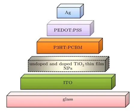
Fig.2.(color online)An inverted configuration of polymer solar cells.
3.Characterization
The structures of pure and vanadium-doped TiO2thinfilm NPs were analyzed using x-ray diffraction(XRD,Model Philips MPD PW 3040)over the 2θ range of 20°–80°at the scan rate of 0.02°/s.The surface morphology of pure and vanadium-doped TiO2thin film NPs was examined by scanning electron microscopy(SEM)and transmission electron microscopy(TEM).The optical properties of the thinfilms were investigated using a UV–VIS–IR(Perkin-Elmer-950 lambda)spectrometer.The current density–voltage characteristics of the cells were measured under AM 1.5 illumination provided by Oriel Sol 1A solar simulator.
4.Results and discussion
The crystalline structure of pure and vanadium-doped TiO2thin films NPs was investigated by XRD.Figure 3(a) shows the XRD pattern of pure TiO2thin film NPs.The diffraction pattern indicates the presence of eight peaks which are attributed to the anatase TiO2crystalline(JCPDS card No.89-492).The eight peaks each are presented in the fields (101),(004),(200),(105),(204),(116),(220),and(215).The XRD pattern of vanadium-doped TiO2thin film NPs is depicted in Fig.3(b).As can be seen,the diffraction peaks move gradually to lower angles due to the vanadium doping of the TiO2thin film.This slight shift towards a lower angle demonstrates doping of TiO2thin film NPs.Also,the eight peaks are attributed to the anatase phase of vanadium-doped TiO2thin films.There are no rutile peaks in both patterns of pure and vanadium-doped TiO2thin films.The peak assigned to the(101)plane is the most intense throughout the pattern, which indicates a preferential orientation of the vanadiumdoped TiO2thin film NPs along the(101)direction.The degree of orientation for the(11)plane is calculated by the relative texture coefficient(χc)[35]

where I0is the peak intensity for a randomly oriented sample. Thus,and χc(215)are calculated to be(0.448,0.435),(0.125,0.166), (0.168,0.136),(0.108,0.117),(0.081,0.070),(0.008,0.018), (0.017,0.020),and(0.045,0.038)for pure and vanadiumdoped TiO2thin films,respectively.These results indicate a preferential orientation of the pure and doped TiO2thin film NPs along the(101)direction.

Fig.3.XRD patterns of(a)pure anatase TiO2 and(b)vanadium-doped TiO2 NPs prepared by the solvothermal method.
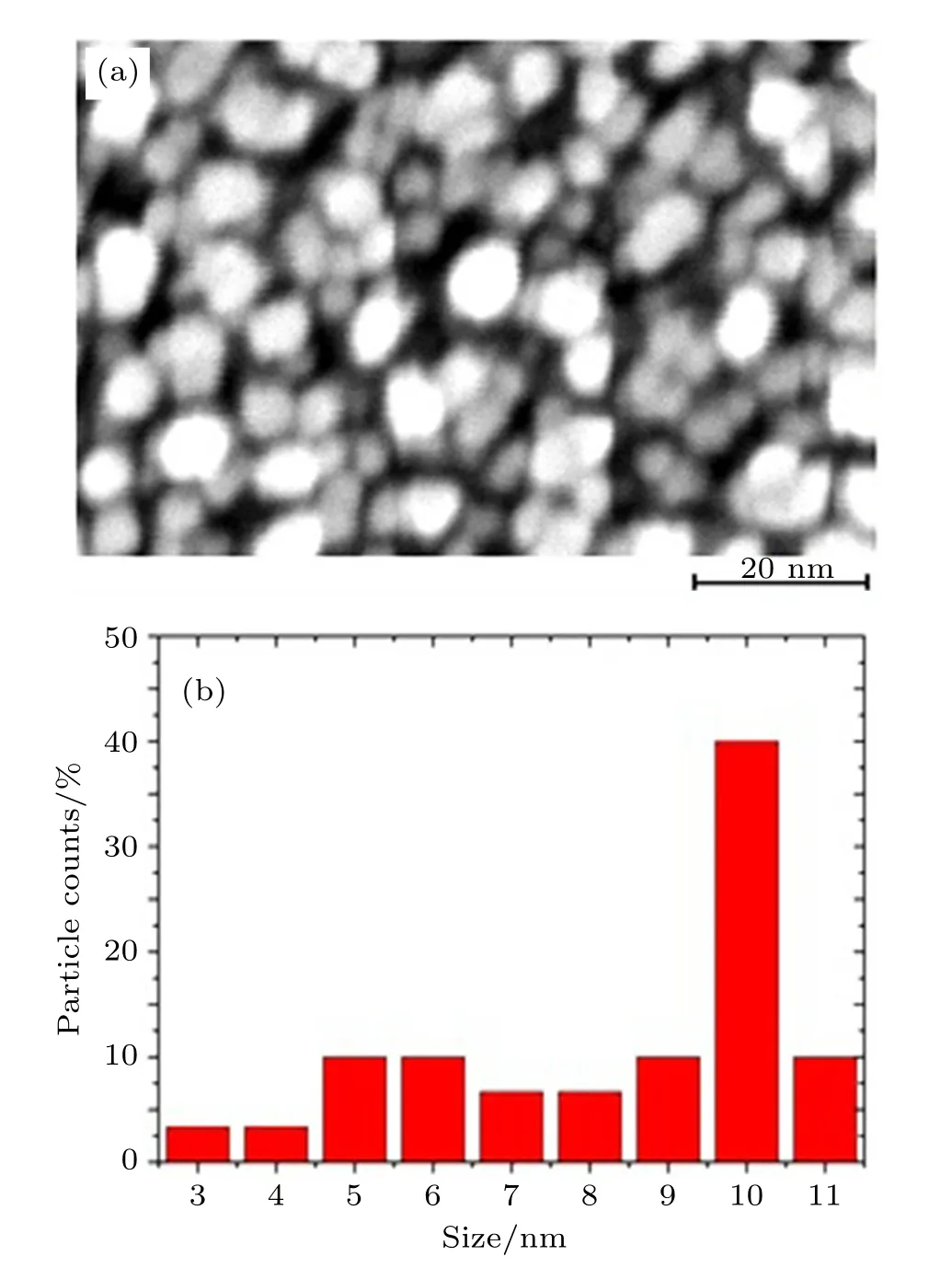
Fig.4.(color online)(a)SEM image and(b)size distribution histogram of TiO2 thin film NPs fabricated via the solvothermal method.
The surface morphology of TiO2thin film NPs is depicted in Figs.4–6.Figure 4 shows(a)the SEM image and (b)the size distribution histogram of TiO2thin films NPs. These images show that TiO2thin film NPs have a size about 10 nm.Figure 5 shows(a)the TEM image and (b)the size distribution histogram of TiO2thin film NPs. The particles are round in shape with good uniform size distribution.Most of the particles have the diameter of about 8 nm.We fabricated our inverted polymer solar cell with the configuration of ITO/pure and vanadium-doped TiO2NPs/P3HT:PCBM/PEDOT:PSS/Ag.The cross-sectional SEM image of the solar cell employed TiO2thin film NPs is shown in Fig.6.This image confirms that the polymer sufficiently infiltrates the interval between nanoparticles.The thickness of the TiO2thin film is 30 nm.

Fig.5.(color online)(a)TEM image and(b)size distribution histogram of TiO2 thin film NPs fabricated via the solvothermal method.

Fig.6.Cross-sectional SEM image of the inverted polymer solar cell with TiO2 NPs.
Optical properties of pure and vanadium-doped TiO2thinfilms with the thickness of 30 nm were measured by a UV–Vis–IR spectrometer,as shown in Fig.7.According to this spectrum,the vanadium-doped TiO2thin film has a high optical transmittance(>70%)in the visible spectrum.

Fig.7.(color online)Transmittance spectra of pure and vanadiumdoped TiO2 thin films with the thickness of 30 nm.
The visible light transmittance decreases for pure TiO2thin film.Thus,the pure TiO2thin film shows lower transmittance than the doped thin film.According to the SEM images, better transmittance might be due to the surface morphology and crystallinity of the thin film.[36–38]The energy band gap of pure and vanadium-doped TiO2thin film NPs is determined using the Tauc formula

where A is a constant,Egis the band gap of the samples and exponent n depends on the type of transition.n=1/2,2,and 3/2 for direct allowed,indirect allowed and direct forbidden transitions,respectively.Here,the transition is direct so we take n=1/2.[39]To measure the energy band gap of pure and vanadium-doped TiO2thin films,from the absorption spectrum a graph of(αhν)2versus(hν)is plotted and extrapolating the straight line portion of(αhν)2to(αhν)2=0 is plotted in Fig.8.The directly allowed band gaps of pure and vanadium-doped TiO2thin film NPs are found to be 3.43 eV and 3.50 eV,respectively.As can be seen,the band gap increases with doping of vanadium.The band gap shift of nanostructure materials in very small NPs is due to the quantum size effect(QSE).According to this effect,with decreasing grain size,the band gap is increased.[37]
Figure 9 shows the J–V curves of the inverted polymersolar cells employing pure and vanadium-doped TiO2thin film NPs under illumination.It shows that the cell using vanadiumdoped TiO2thin film NPs has the best J–V performance.The solar cells using vanadium-doped thin film NPs show better J–V performance compared to their thickness counterparts,and this confirms the effectiveness of using vanadium as a dopant in cells.Vocof the polymer fullerene is heavily dependent on the energy difference between the HOMO level of the donor and the LUMO level of the acceptor,so all of the cells use the same active layer,their Vocare the same.[40]Table 1 shows the extracted data of the fabricated cells.As predicted,the cells with vanadium-doped TiO2thin film NPs show higher efficiencies.The cell using vanadium-doped thin film NPs with thickness 60 nm has an efficiency∼0.42%higher than its pure counterpart.The cell with 30 nm vanadium-doped TiO2thin film NPs has the highest efficiency of 3.68%,but the pure TiO2thin film with the same thickness shows an efficiency of 2.95%and this is because of the lower conductivity of the pure TiO2thin film.It is remarkable to see that even with Jscof 10.70 mA/cm2,the cell could not reach a higher efficiency.As the fill factor depends on the series resistance, for achieving higher PCEs even at this thickness,higher fill factors must be achieved.This somehow shows that at higher thicknesses,increasing the series resistance causes a loss in power conversion efficiency and in lower thicknesses while the series resistance is low,the lack of good interfacial area with active layer prevents the cell from having higher performance and this puts a higher power conversion efficiency limit in the thickness of 30 nm thin films.Also lower fill factor is another criterion affecting the performance of the cell.External quantum efficiency(EQE)of cells plays a great role in confirming the efficiency of cells and is a key parameter for characterizing solar cell performance under different conditions.[9]Figure 10 shows the EQE curves of the cells using pure and vanadiumdoped TiO2thin films NPs.Doped TiO2thin film NPs are superior to their pure counterpart.Considering that the integration of EQE should be proportional to Jsc,there is consistency between data obtained from the EQE curve and the solar simulator.Curves also show the decreases of the efficiency of these cells for wavelengths longer than 600 nm.So by enhancing the cell with materials that can absorb longer wavelengths, the cell performance can be improved.

Fig.8.(color online)Optical band gap of(a)pure and(b)vanadiumdoped TiO2 thin film NPs.
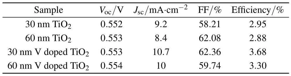
Table 1.Key parameters of inverted polymer solar cells under illumination.

Fig.9.(color online)J–V curves of devices using pure and vanadiumdoped TiO2 thin films with different thicknesses.

Fig.10.(color online)External quantum efficiency of the cells with the best efficiency.
5.Conclusion
Employing vanadium-doped TiO2thin film NPs as the electron transport layer was effective and it improved the optical and electrical performance of the cells.Best thickness of our pure and vanadium-doped thin films was 30 nm.The cell using 30 nm vanadium-doped TiO2thin films achieved 3.68% power conversion efficiency with Jscof 10.7 mA/cm2and Vocof 0.553.The fill factor of this cell was 62.36%.This somehow shows that at higher thicknesses,increase of series resistance causes a loss in power conversion efficiency and in lower thicknesses while the series resistance is low,but the lack of good interfacial area with active layer prevents the cell from having higher performances and this puts a higher power conversion efficiency limit in the thickness of 30 nm thin films; also lower fill factor is another criterion affecting the performance of cell.So we suggest using other forms of vanadiumdoped TiO2,like nanorods and nanotubes.
[1]N Yeh and Yeh P 2013 Renew.Sustainable Energy Rev.21 421
[2]Capasso A,Salamandra L,Chou A,Carlo A D and Motta N 2014 Sol. Energ.Mat.Sol.C 122 297
[3]M A Ibrahem,h Y Wei,M H Tsai,K C Ho,J J Shyue and C W Chu 2013 Sol.Energ.Mat.Sol.C 108 156
[4]Jin F 2013 Sol.Energ.Mat.Sol.C 117 189
[5]Noh Y J,Na S I and Kim S S 2013 Sol.Energ.Mat.Sol.C 117 139
[6]Sio A D,Chakanga K,Sergeev O,Maydell K V,Parisi J and Hauff E V 2012 Sol.Energ.Mat.Sol.C 98 52
[7]Zhang B,Lee D H,Chae H,Park C and Cho S M 2010 Korean J.Chem. Eng.27 999
[8]Lee S B 2013 Sol.Energ.Mat.Sol.C 117 203
[9]Ahmadi M,Mirabbaszadeh K,Salari S and Fatehy H 2014 Electron. Mater.Lett.10 951
[10]Hu Z,Zhang J and Zhu Y 2013 Sol.Energ.Mat.Sol.C 117 610
[11]Mirabbaszadeh K,Ahmadi M,Khosravi M,Mokhtari R and Salari S 2013 J.Inorg.Organomet.Polym.23 1219
[12]Ahmadi M and Rashidi D S 2015 Chin.Phys.B 24 11723
[13]Jiang Z L 2013 Sci.China.Chem.56 1573
[14]Harrison L R and Bruce H R 2007 J.Phys.Chem.C 111 18765
[15]Wiranwetchayan O,Liang Z,Zhang Q,Cao Gand SingjaiP 2011 Mate. Sci.Appl.2 1697
[16]Brabec C J,Shaheen S E,Winder C,Sariciftci N S and Denk P 2002 Appl.Phys.Lett.80 1288
[17]Liao H H,Chen L M,Xu Z,Li G and Yang Y 2008 Appl.Phys.Lett. 92 17 3303
[18]Lee Y I,Youn J H,Ryu M S,Kim J and Moon H T 2011 J.Jang.Org. Electron.12 353
[19]Zhao D W 2010 Sol.Energ.Mat.Sol.C 94 985
[20]Jorgensen M,Norrman K and Krebs F C 2008 Sol.Energ.Mat.Sol.C 92 686
[21]Schattauer S 2012 Colloid.Polym.Sci.290 1843
[22]Peng R,Yang F,Ouyang X,Liu Y,Kim Y S and Ge Z 2014 Appl.Phys. A 114 429
[23]Lee J and Jho J Y 2011 Sol.Energ.Mat.Sol.C 95 3152
[24]Kim D 2014 Ceram.Int.40 1457
[25]Saehana S,Prasetyowati R,Hidayat M I,Arifin P,Khairurrijal and Abdullah M 2011 IJBAS 11 15
[26]Quan W,Cheng C,Liu J,Zhang J,Yan D and Qin D 2011 Appl.Phys. A 104 47
[27]Sio A D,Chakanga K,Sergeev O,Maydell K V,Parisi J and Hauff E V 2012 Sol Energ.Mat.Sol.C 98 52
[28]Stubhan T,Oh H,Pinna L,Krantz J,Litzov I and Brabec C J 2011 Org. Electron.12 1539
[29]Ihn S G 2011 Sol.Energ.Mat.Sol.C.95 1610
[30]Pal E,Hornok V,Oszkoo A and Dekany I 2009 Colloid Surf.A 340 1
[31]Fei H,Fang M,Tao L and Guangxing L 2013 Chin.J.Catal.34 2263
[32]Li L,Liu C Y and Liu Y 2009 Mater.Chem.Phys.113 551
[33]Liu Y 2010 ACS Nano 4 5373
[34]Feng X,Shankar K,Paulose M and Grimes C A 2009 Angew.Chem. Int.Ed.48 8095
[35]Samanta P K,Basak S and Chaudhuri P R 2011 Inter.J.Nano Sci.1 69
[36]Asmar R A,Zaouk D,Bahouth P,Podleki J and Foucaran A 2006 Microelectron.Eng.83 393
[37]Salari S,Ahmadi M and Mirabbaszadeh K 2014 Electron.Mater.Lett. 10 13
[38]J H Lee,K H Ko and B O Park 2003 J.Cryst.Growth.247 119
[39]Reddy K M,Manorama S V and Reddy A R 2002 Mater.Chem. Physics.78 239
[40]Brabec C j,Dyakonov V,Parisi J and Sariciftci N S 2003 Organic Photovoltaics:Concepts and Realizatio n(Heidelberg:Springer-Verlag Berlin)
12 March 2017;revised manuscript
13 May 2017;published online 18 July 2017)
10.1088/1674-1056/26/9/097203
†Corresponding author.E-mail:m.ahmadi@vru.ac.ir
©2017 Chinese Physical Society and IOP Publishing Ltd http://iopscience.iop.org/cpb http://cpb.iphy.ac.cn
杂志排行

Chinese Physics B的其它文章
- Improved control for distributed parameter systems with time-dependent spatial domains utilizing mobile sensor actuator networks∗
- Geometry and thermodynamics of smeared Reissner–Nordström black holes in d-dimensional AdS spacetime
- Stochastic responses of tumor immune system with periodic treatment∗
- Invariants-based shortcuts for fast generating Greenberger-Horne-Zeilinger state among three superconducting qubits∗
- Cancelable remote quantum fingerprint templates protection scheme∗
- A high-fidelity memory scheme for quantum data buses∗