Simulation of Gain Properties for Slot Waveguide Amplifiers Based on Erbium-doped Polymers
2017-02-13LITongZHANGMeilingWANGFeiZHANGDamingWANGGuoping
LI Tong,ZHANG Mei-ling,WANG Fei∗,ZHANG Da-ming,WANG Guo-ping
(1.College of Electronic Science and Technology and Guangdong Provincial Key Laboratory of Micro/Nano Optomechatronics Engineering and Key Laboratory of Optoelectronic Devices and Systems of Ministry of Education and Guangdong Province,Shenzhen University,Shenzhen 518060,China;2.State Key Laboratory on Integrated Optoelectronics,Engineering Laboratory on Polymeric Waveguide Components of Optics Communications of Jilin Province,College of Electronic Science and Engineering,Jilin University,Changchun 130012,China)∗Corresponding Author,E-mail:wang_fei@jlu.edu.cn
Simulation of Gain Properties for Slot Waveguide Amplifiers Based on Erbium-doped Polymers
LI Tong1,ZHANG Mei-ling2,WANG Fei2∗,ZHANG Da-ming2,WANG Guo-ping1
(1.College of Electronic Science and Technology and Guangdong Provincial Key Laboratory of Micro/Nano Optomechatronics Engineering and Key Laboratory of Optoelectronic Devices and Systems of Ministry of Education and Guangdong Province,Shenzhen University,Shenzhen 518060,China;2.State Key Laboratory on Integrated Optoelectronics,Engineering Laboratory on Polymeric Waveguide Components of Optics Communications of Jilin Province,College of Electronic Science and Engineering,Jilin University,Changchun 130012,China)∗Corresponding Author,E-mail:wang_fei@jlu.edu.cn
A slot waveguide amplifier based on high concentration erbium-doped polymers,working at 1 550 nm wavelength under 1 480 nm pumping,is presented to realize high optical gains with low pump powers for the loss compensation in the silicon-based optical interconnection.The influence factors of the gain properties,such as the optical properties of the polymers,the structure sizes of the slot waveguides,and the signal and pump powers,are numerically simulated.This structure,with the nanometer scale,only needs a 1.5 mW pump to obtain a 4.5 dB gain,which exhibits promising applications in integrated optical systems.Further,multiple-layer slot structures are introduced to get higher gains,and the over-lapping integral factor of the four-layer slot waveguides is 42%larger than that of the one-layer waveguides.
waveguide amplifier;slot waveguide;optoelectronic device
关 键 词:波导放大器;狭缝波导;光电子器件
1 Introduction
Silicon-based on-chip optoelectronic devices,with advantages of high speed,large bandwidth,and compatibility with CMOS process,have attracted much attention recently[1-4].Great breakthroughs have been achieved,such as lasers,modulators,photoelectric detectors,and so on[5-7].However,there are many challenges in the interconnection with low loss for the integrated optical system.The waveguide amplification technology,which can amplify optical signals without any light-to-electricity conversion,is a very effective method for loss compensations in the optical interconnection network. Compared with the traditional Raman amplifiers[8-9],rare-earth-doped waveguide amplifiers have excellent properties such as low pump powers,high gains,and simple structures.The gain materials with inorganic host,such as lithium niobate crystals,phosphate glass,and oxide thin films,suffer from complicated manufacturingprocess,highproduction costs,and poor compatibility with silicon material. Conversely,rare-earth-doped polymers become good candidates for waveguide amplifiers,due to the controllability of their refractive indices and the large variety of species.
However,the cross section sizes of polymer waveguidesareusuallylarge,inthemicron scale[10-11],because the refractive indexes of the polymers are relatively low,which is hardly suited to high-density integration.In this letter,in order to overcomethisissue,akindofsilicon-based waveguide amplifier at 1 550 nm wavelength under 1 480 nm pumping is presented by combining silicon slot waveguide structures with a high concentration erbium-doped(Er3+-doped)polymer active medium.The slot waveguides[12-14],which have much smaller cross sections(nanometer scale),can confine the optical field into the narrow low-refractiveindex slot regions.It will lead to an extremely high optical intensity in the polymer gain medium,which is beneficial to get high optical gains with low pump powers.Besides,in this structure,the advantages of polymers for waveguide amplifiers are retained.We analyze the gain properties of the waveguide amplifiers by setting up the rate equations and propagation equations of the optical power based on the optical amplifying theory of excited emission and a four-level system model for Er3+ions.The influence factors of the gain properties,such as the optical properties of the polymers,the structure sizes of the slot waveguide,and the signal and pump powers,have been numerically simulated.This kind of waveguide amplifier can obtain high optical gains with extremely low pump power.In addition,multiple-layer structure is designed to further increase the gain.
2 Theoretical Model
The slot waveguides,composed of a narrow lowrefractive-index slot sandwiched between two high-refractive-index materials,can realize a strong light confinement(the transverse electric optical mode,where the electric field is parallel to the wafer plane and orthogonal to the direction of propagation)in the slot region.Since the normal component of the electric flux density,D=n2e0E(where n and e0are the refractive index and the vacuum permittivity,respectively),to satisfy the continuity of D at the high-index-contrast interface,the corresponding discontinuous electric field E will be formed with much higher amplitude in the nanometer-wide and low-index side(nlow)and lower amplitude in the high-index side(nhigh)[15].Fig.1(a) illustrates the physical model for the horizontal component of the electric field(Ex)distribution of the slot waveguides filled with polymers.Here,the height of silicon(hSi)and the widths of silicon(wSi)and the slot(wS)are 250,200 and 50 nm,respectively.The refractive indices of corresponding region are nSiO2=1.46,nSi=3.48 and npoly=1.58,respectively.The Exfield eigenmode is calculated by finite element method simulations[16].The Exfield distribution of 1 550 nm signal light in the slot waveguide is shown in Fig.1(a)by the color contour and in Fig.1(b) by the three-dimensional surface plot.One can findthat the peak amplitude of the Exfield in the slot region is much higher than those in the silicon and the cladding regions.
With respect to the rare-earth-doped polymer waveguide amplifiers,many efforts have been devoted to the synthesis of exceptional active materials[17-18].Here,a solution-processable erbium-ytterbium co-doped complex film which has a high erbium concentration of 10.8%(mass fraction)is used as the low-index filler.Using this complex material as the high-index core,we have obtained a 6.5 dB relative optical gain of the 1 550 nm wavelength light in an embedded waveguide pumped at 980 nm wavelength[19].By spin coating this complex solution onto a prepared slot waveguide and then drying it,the polymer-based slot waveguide amplifier can be obtained.Fig.1(c)-(e)show the scanning electron microscope(SEM)images of 500 nm slot waveguide without polymer,the cross section of the 200 nm and 80 nm slot waveguides with the complex filled in them,respectively.It is evident that this erbiumdoped complex has excellent filling properties to the nano-slots.To avoid the excess 980 nm pump absorption of the silicon layers[20],we simulated the gain property at 1 480 nm pumping.Besides,the Yb3+ions can't function as sensitizer at 1 480 nm pumping,so the synthesis of the complex would be adjusted to only Er3+ions doping.

Fig.1 Color contour(a)and three-dimensional surface plot(b)of amplitude distribution of the horizontal component of the electric field(Ex)of a slot waveguide.(c)Scanning electron microscope(SEM)image of 500 nm slot waveguide without polymer.(d)-(e)SEM image of the cross section of the 200 nm(d)and 80 nm(e)slot waveguides with the polymer filled in.The size of silicon is 250 nm×200 nm.
Afour-levelsystemmodelforEr3+-doped waveguide amplifier is established to calculate the optical gain of the slot waveguide amplifier.In the theory analysis,we take into account the cooperative upconversion due to an interaction of two Er3+ions in the state4I13/2,and the excited state absorption (ESA)[21]from the4I13/2state to the4I9/2state.The influence of amplified spontaneous emission(ASE) is neglected.In order to simplify the simulation,the over-lappingintegralbetweentheopticalfield (pump or signal)and the Er3+ion distribution is adopted.Assuming the Er3+ions in the active materials are uniformly-doped,the over-lapping integral factors(Γp,s)are expressed as[22]:

where,A is the doping area,Ψp,sis the distribution of the normalized light intensity,and the subscripts p and s separately represent the pump light and the signal light.In the slot waveguide structure,the area A,ignoring the effect of the polymer cladding,is the cross section area of the slot region.Therefore,Γp,srepresent the optical power in the slot region which are normalized with respect to the total waveguide optical power.
3 Results and Discussion
For the sake of high gains in the slot waveguide amplifier,the waveguide gain as a function of pump power for different influence factors is numerically analyzed and shown in Fig.2.Here,the waveguide gain,G(dB)is calculated using Eq.(2)[22]:

where,Ps(0)and Ps(L)are the signal powers at the input point and the output point of the waveguide,respectively.The parameters of the model used in the calculation are shown in Tab.1[22-24].

Tab.1 Main parameters used in the calculations
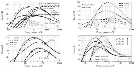
Fig.2(a)shows the optical gain has a maximum value,but does not get saturated with the increase of pump power(Pp)by considering the ESA.Therefore we can get an optimum pump (Pp-opti)to acquire the best gain of the amplifier. One can also see in Fig.2(a)that the gain increases while the cooperative upconversion(Cup)decreases or the Er3+ion concentration(NEr)increases.The Cupand NErare subject to the active material,so the lower Cupand larger NErare the selection criteria.Fig.2(b)illustrates the influence of the wavelength loss on the optical gain at different waveguide length(L).As seen in Fig.2(b),although the increment of L brings a gain increasing,Pp-optiwill dramatically increase with it.As a result, L requires careful consideration of Ppconstraints,and is not the longer the better.From Fig.2(c),one can find that the smaller the signal power(Ps)propagating in the waveguide is,the larger the maximum gain is.The influence of the cross section area of the active region(A)on the gain,Pp-optidecreases with A,is demonstrated in Fig.2(d).Obviously,the slot waveguide has an advantage of pump efficiency for its A is very small.From Fig.2(d),we also find Γp,splay crucial roles on the gain,which can be used to characterize the gain property.However,Γp,s,different from other parameters,are related to the structure of waveguides.In order to acquire the high gain of the slot waveguide,it is necessary to optimize the size to get large Γp,s.

Fig.2 Numerical simulation of the optical gain at 1 480 nm pumping.The gain as a function of the pump power at different factors:(a)Cup,ESA,and NEr.(b)L,Kp,and Ks.(c)Ps.(d)A and Γp,s.

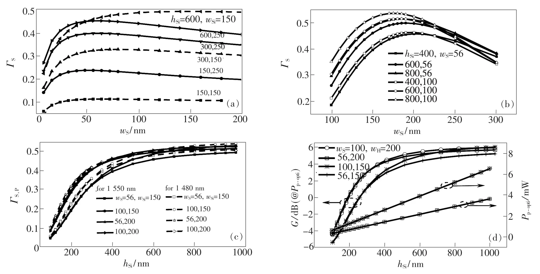
Fig.3 Size optimizing of the slot waveguides for the high gain and low pump power.The over-lapping integral factor Γp,sas a function of(a)wS,(b)wSiand(c)hSiwhile keeping other parameters constant.(d)The maximum gain and its corresponding Pp-optiat optimum wSand wSi.
Assuming the refractive-index distribution is fixed,the over-lapping integral factors Γp,sare determined by the size of the slot waveguide:wSi,wS,and hSiin Fig.1(a).Due to the relation between Γp,sand the gain property,we optimize these size parameters in Fig.3.Fig.3(a)shows the over-lapping integral factor of the signal light(Γs)as a function of wS,which indicates Γsremains nearly constant for wS>56 nm at different wSiand hSi.In order to get preferred wSiand hSi,we chose wS=56 nm and wS=100 nm in the following simulations. Fig.3(b)shows the relation between the Γsand wSiat different hSi.The Γshas maximal values as wSiis around 150-200 nm.Further,wSi=150 nm and wSi=200 nm are chosen to acquire the optimal hSi. As seen in Fig.3(c),the Γshas reached a saturation point in increasing hSi.The over-lapping integral factor of the pump light(Γp)is also presented in Fig.3(c).On this basis,according to the relation between Pp-optiand the section A of the slot,weget the maximum gain results and the corresponding Pp-optias a function of hSi,which is shown in Fig.3 (d).When wS=56 nm,wSi=200 nm,and hSi=400 nm at the condition of Kp=Ks=1 dB/cm,the slot waveguide amplifier achieves a 4.5 dB optical gain,while only a 1.5 mW power of 1 480 nm pump is needed,which is much lower than that in a conventional high-index waveguide[22].

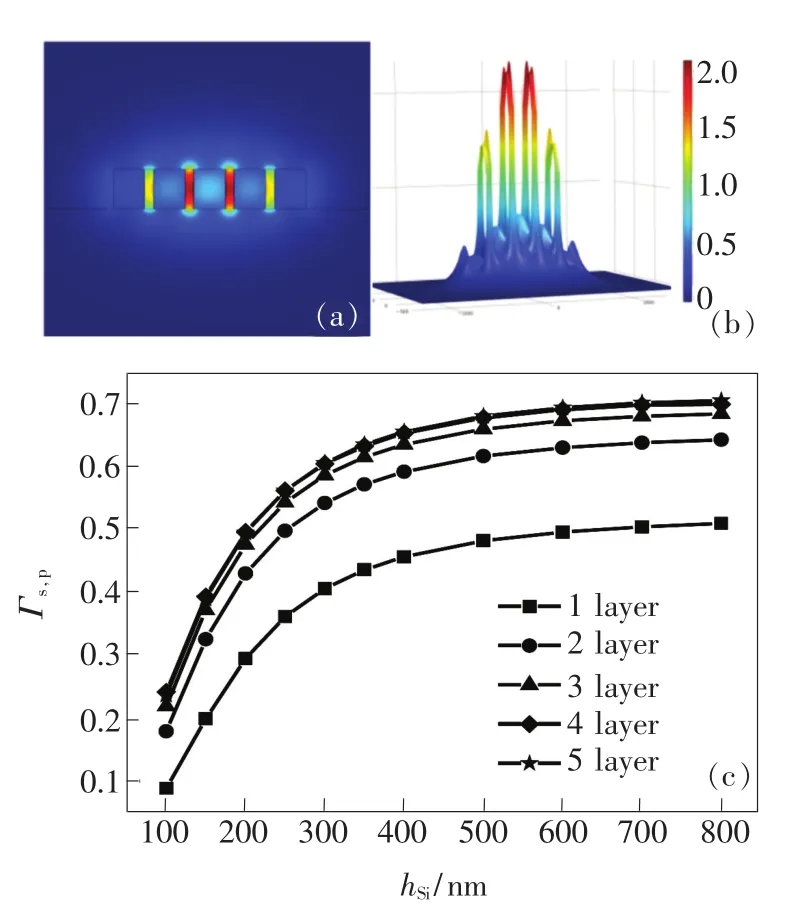
Fig.4 Structure optimizing of the slot waveguides for the high gain.(a)Color contour and(b)three-dimensional surface plot of the Exfield amplitude of fourlayer slot waveguide while wS=56 nm and wSi=200 nm.(c)The over-lapping integral factor Γsas a function of hSiat different layer numbers.
Further,the structure that consists of multiple low-index nanometer thin layers sandwiched by highindex silicon is introduced in the slot-waveguide amplifier for enhancing Γp,s.The Exfield distribution of the four-layer slot waveguide as an example is illustrated in Fig.4(a)and(b).The simulation result of Fig.4(c)obviously demonstrates the Γsis augmented by increasing the number of layers,and becomes saturated at last.Thus three-layer or fourlayer slot is advisable.When hSi=500 nm,the Γsof the four-layer slot waveguide is 0.68,42%larger than that of the one-layer slot waveguide.It indicates this method is an effective means to increase the optical gain of the slot-waveguide amplifier.
4 Conclusion
We demonstrate a silicon slot-waveguide amplifier based on erbium-doped polymers,which can be easily fabricated and has well compatibility with CMOS process.By numerical simulation,the influences of the various physical parameters on the optical gain are analyzed.We find that this kind of waveguide amplifier realizes using extremely low pump powers to obtain high gains.To obtain larger gain,the size of the slot waveguide is optimized to enhance the over-lapping integral factor.Finally,the method of multiple-layer structure is proposed to further increase the gain.
[1]CHEN R,TRAN T T D,NG K W,et al..Nanolasers grown on silicon[J].Nat.Photon.,2011,5(3):170-175.
[2]ZHANG L,YANG M,JIANG Y T,et al..Architectures and routing schemes for optical network-on-chips[J].Comput. Electr.Eng.,2009,35(6):856-877.
[3]CHEN G Q,CHEN H,HAURYLAU M,et al..Predictions of CMOS compatible on-chip optical interconnect[J].Integration VLSI J.,2007,40(4):434-446.
[4]YAN Z X,LI C H,LUO Y,et al..Silver hierarchical structures grown on microstructured silicon in chip for microfluidic integrated catalyst and SERS detector[J].Chin.Opt.Lett.,2015,13(10):102401-1-5.
[5]TANG L,KOCABAS S E,LATIF S,et al..Nanometre-scale germanium photodetector enhanced by a near-infrared dipole antenna[J].Nat.Photon.,2008,2(4):226-229.
[6]RONG H S,XU S B,KUO Y H,et al..Low-threshold continuous-wave Raman silicon laser[J].Nat.Photon.,2007,1(4):232-237.
[7]LIU A S,LIAO L,RUBIN D,et al..High-speed optical modulation based on carrier depletion in a silicon waveguide [J].Opt.Express,2007,15(2):660-668.
[8]SINGH A.Influence of carrier transport on Raman amplification in silicon waveguides[J].Opt.Express,2010,18(12):12569-12580.
[9]SIH V,XU S B,KUO Y H,et al..Raman amplification of 40 Gb/s data in low-loss silicon waveguides[J].Opt.Express,2007,15(2):357-362.
[10]CAI Z Z,YU H Y,ZHANG Y C,et al..Synthesis and characterization of novel fluorinated polycarbonate negative-type photoresist for optical waveguide[J].Polymer,2015,61:140-146.
[11]WAN Y,ZHANG Y,SHI Z S,et al..Direct UV-written highly fluorinated aromatic-aliphatic copolyethers for optical waveguides[J].Polymer,2012,53(4):967-975.
[12]MANN V,ASHOK N,RASTOGI V.Coupled strip-slot waveguide design for dispersion compensation[J].Opt.Quant. Electron.,2015,47(9):3161-3169.
[13]CHENG N C,MA Y F,FU P H,et al..Horizontal slot waveguides for polarization branching control[J].Appl.Opt.,2015,54(3):436-443.
[14]YIN H Z,LIU Y M,YU Z Y,et al..Nonlinear hybrid plasmonic slot waveguide for second-harmonic generation[J]. Chin.Opt.Lett.,2013,11(10):101901-1-5.
[15]ALMEIDA V R,XU Q F,BARRIOS C A,et al..Guiding and confining light in void nanostructure[J].Opt.Lett.,2004,29(11):1209-1211.
[16]TORRISI G,MASCALI D,SORBELLO G,et al..Full-wave FEM simulations of electromagnetic waves in strongly magnetized non-homogeneous plasma[J].J.Electromagnet.Wave Appl.,2014,28(9):1085-1099.
[17]LEI K L,CHOW C F,TSANG K C,et al..Long aliphatic chain coated rare-earth nanocrystal as polymer-based optical waveguide amplifiers[J].J.Mater.Chem.,2010,20(35):7526-7529.
[18]LIU X Y,CHEN X,ZHAI X S,et al..NaYF4nanocrystals with intense 1 530 nm fluorescence for polymer optical waveguide amplifiers[J].J.Nanosci.Nanotechnol.,2014,14(5):3499-3502.
[19]CHEN C,ZHANG D,LI T,et al..Erbium-ytterbium codoped waveguide amplifier fabricated with solution-processable complex[J].Appl.Phys.Lett.,2009,94(4):041119-1-3.
[20]PINTUS P,FARALLI S,DI PASQUALE F.Integrated 2.8 μm laser source in Al2O3∶Er3+slot waveguide on SOI[J]. J.Lightwave Technol.,2011,29(8):1206-1212.
[21]BROWN E E,HÖMMERICH U,BLUIETT A,et al..Near-infrared and upconversion luminescence in Er∶Y2O3ceramics under 1.5 μm excitation[J].J.Am.Ceram.Soc.,2014,97(7):2105-2110.
[22]LI T,LIU T,CHEN C,et al..Gain characteristics of LaF3∶Er,Yb nanoparticle-doped waveguide amplifier[J].J. Nanosci.Nanotechno.,2011,11(11):9409-9414.
[23]PINTUS P,FARALLI S,DI PASQUALE F.Low-threshold pump power and high integration in Al2O3∶Er3+slot waveguide lasers on SOI[J].IEEE Photon.Technol.Lett.,2010,22(19):1428-1430.
[24]CHEN K X,CHU P L,CHIANG K S,et al..Design and fabrication of a three-dimensional polymer optical waveguide polarization splitter[J].Opt.Commun.,2005,250(4-6):297-301.

李彤(1984-),女,吉林长春人,博士后,2012年于吉林大学获得博士学位,主要从事平面光波导放大器的研究。
E-mail:litong0722@foxmail.com

王菲(1978-),女,黑龙江哈尔滨人,博士,副教授,2005年于吉林大学获得博士学位,主要从事平面光波导集成器件的研究。
E-mail:wang_fei@jlu.edu.cn
掺铒聚合物狭缝波导放大器的增益特性研究
李 彤1,张美玲2,王 菲2∗,张大明2,汪国平1
(1.深圳大学电子科学与技术学院,广东省微纳光机电工程技术重点实验室,光电子器件与系统教育部/广东省重点实验室,广东深圳 518060;2.吉林大学电子科学与工程学院,集成光电子学国家重点联合实验室吉林大学实验区,吉林省光通信用聚合物波导器件工程实验室,吉林长春 130012)
设计了一种高浓度稀土铒掺杂聚合物填充硅狭缝结构的平面光波导放大器(工作波长1 550 nm,泵浦波长1 480 nm),能够在低泵浦下获得高增益,可以应用于硅基光互联的损耗补偿。通过扫描电镜照片观察发现,合成的铒掺杂聚合物材料具有良好的纳米狭缝填充能力。考虑铒离子的合作上转换和激发态吸收,利用铒离子四能级跃迁模型,建立原子速率方程和光功率传输方程,数值仿真分析了聚合物光学性质、狭缝波导结构参数及信号光泵浦光功率等放大器增益特性的影响因素。这种具有纳米截面尺寸的光波导放大器,获得4.5 dB的信号光相对增益仅需要1.5 mW的泵浦光,展现了良好的集成光学应用前景。为了进一步提高增益,引入了多层狭缝结构,四层狭缝波导的重叠积分因子比一层狭缝的高42%。
2016-08-04;
2016-09-02
国家自然科学基金(11274247,11574218,11504243,61475061);广东省自然科学基金(2016A030313042,2015A030310400)资助项目Supported by National Natural Science Foundation of China(11274247,11574218,11504243,61475061);Natural Science Foundation of Guangdong Province(2016A030313042,2015A030310400)
TN256
A
10.3788/fgxb20173802.0213
1000-7032(2017)02-0213-07
