PbO-PbI2复合物膜转化的CH3NH3PbI3钙钛矿薄膜及其光电特性
2015-12-29丁绪坤李效民高相东张树德黄宇迪李浩然中国科学院上海硅酸盐研究所高性能陶瓷和超微结构国家重点实验室上海200050
丁绪坤 李效民 高相东 张树德 黄宇迪 李浩然(中国科学院上海硅酸盐研究所,高性能陶瓷和超微结构国家重点实验室,上海200050)
PbO-PbI2复合物膜转化的CH3NH3PbI3钙钛矿薄膜及其光电特性
丁绪坤 李效民*高相东 张树德 黄宇迪 李浩然
(中国科学院上海硅酸盐研究所,高性能陶瓷和超微结构国家重点实验室,上海200050)
有机-无机卤化物钙钛矿是一类优异的光电材料.在过去四年内,基于有机-无机卤化物钙钛矿的光电器件实现了超过15%的光电转换效率.而有机-无机卤化物钙钛矿材料的可控制备是保证其在光电器件中应用的基础.本文采用新的沉积方法在玻璃衬底表面制备了一种典型的有机-无机卤化物钙钛矿CH3NH3PbI3薄膜.其制备过程是:采用超声辅助的连续离子吸附与反应法在玻璃衬底表面沉积PbO-PbI2复合物膜,之后与CH3NH3I蒸汽在110°C环境下反应,将PbO-PbI2复合物膜转化成CH3NH3PbI3钙钛矿薄膜.对CH3NH3PbI3薄膜的微观结构,结晶性及其光电性能等进行了表征.结果表明,CH3NH3PbI3薄膜呈晶态,具有典型的钙钛矿晶体结构.薄膜表面形貌均匀,晶粒尺寸超过400 nm.在可见光范围,CH3NH3PbI3薄膜透过率低于10%,能带宽度为1.58 eV.电学性能研究表明CH3NH3PbI3薄膜表面电阻率高达1000 MΩ.高表面电阻率表明CH3NH3PbI3薄膜具有一定的介电性能,其介电常数(εr)在100 Hz时达到155.本研究提出了一种制备高质量CH3NH3PbI3钙钛矿薄膜的新方法,所得CH3NH3PbI3薄膜可望在光、电及光电器件中得到应用.
CH3NH3PbI3;薄膜;钙钛矿;连续离子吸附与反应法;气相过程;光电材料
©Editorial office ofActa Physico-Chimica Sinica
Key Words:CH3NH3PbI3;Thin film;Perovskite;Successive ionic layer adsorption and reaction; Vapor process;Photovoltaic material
1 Introduction
Organic-inorganic halide perovskites CH3NH3PbX3(X=Cl,Br, I)have recently attracted great attention due to their special physical and chemical properties.There are some organic-inorganic halide perovskites(CH3NH3PbI3,CH3NH3PbIxCl3-x,CH3NH3PbIxBr3-x) having been vastly investigated.Among them,CH3NH3PbI3is considered as an ideal absorber in photovoltaic devices due to its narrow band gap,1high absorption coefficient,2near-perfect crystallinity,and excellent electron and hole transport.3Although first implemented in dye-sensitized solar cells based on mesoporous structures,4-6CH3NH3PbI3has been gradually found to assume planar architecture solar cells.7-9Therefore significant efforts have been made to enhance controllability of CH3NH3PbI3thin film quality for constructing high performance planar structure devices.
Several techniques,such as co-evaporation of two precursors,9,10solution-based spin-coating,11,12vapor-assisted solution process,13have been developed to prepare CH3NH3PbI3thin films.However, co-evaporation demands sophisticated equipment which hinders mass production and spin-coating often results in incomplete surface coverage.It is also difficult for vapor-assisted solution process to find suitable solvents which can dissolve PbI2at room temperature.13Hence,in views of low cost and non-solution spincoating process,there is an urge to develop a simple approach for fabricating CH3NH3PbI3thin films.
Successive ionic layer adsorption and reaction(SILAR)technique for deposition of thin films is based on a heterogeneous reaction between adsorbed ions and solvated ions on the solidliquid interface.14With outstanding features of low-cost,the simplicity of procedure and high quality of obtaining films,SILAR technique has been widely applied to prepare kinds of semiconductor films,for instance PbS,15Cu2S,16CdS,17ZnO,18In2S3,19and the like,on various substrates.On the other hand,ultrasonic has been introduced to SILAR technique because of the nature of high energy field and cavitations20etc.Further researches show that ultrasonic-assisted SILAR technique reveals thin films with smoother and more compact surface morphology compared with the traditional SILAR method because the former can remove the loose particles effectively.21
In this article,we fabricated CH3NH3PbI3thin films by reacting ultrasonic-assisted SILAR derived PbO-PbI2hybrid films with CH3NH3I vapor at high temperature of 110°C.The key step was that PbO-PbI2hybrid films were deposited on glass slide substrates by ultrasonic-assisted SILAR technique.CH3NH3PbI3thin films then were prepared via the in-situ reaction of the hybrid films with CH3NH3I vapor at 110°C,which led to the formation of uniform and compact CH3NH3PbI3thin films on substrates.The deposition mechanism of CH3NH3PbI3thin films was investigated by X-ray diffraction(XRD),scanning electron microscopy(SEM), and energy dispersive X-ray spectroscopy(EDS).Optical and electrical properties of thin films were also presented.
2 Experimental
2.1 Materials
Chemicals used in this work including lead nitrate(PbNO3,≥99%),ethanolamine(C2H7NO,≥99%),sodium iodide(NaI,≥99%)were used without further purification.CH3NH3I was synthesized according to reported procedure.24 mL methylamine (CH3NH2,33%(w)in alcohol,Sigma)and 10 mL hydroiodic acid (HI,57%(w)in water,Aldrich)reacted in 250 mL round bottomed flask at 0°C for 2 h with stirring.The precipitate was recovered by evaporation on a rotary evaporator at 60°C for 1 h. The yellow raw product was washed with diethyl ether(C4H10O,≥99.5%)and repeated three times.After drying at 60°C in vacuum oven over 24 h,white solid CH3NH3I was obtained.
2.2 Preparation of CH3NH3PbI3thin films
The glass slides were chosen as substrates and cleaned by ultrasonic in deionized water,ethanol,and acetone sequentially for 15 min and dried under a nitrogen flow before used.
In ultrasonic-assisted SILAR procedure,aqueous solutions of lead nitrate complex with ethanolamine(ETA)and sodium iodide were used as precursors.The concentrations of the solutions were 0.1 and 0.2 mol·L-1,respectively.In a representative cycle of ultrasonic-assisted SILAR procedure,substrates were immersed into lead ion(Pb2+)precursors,iodide ion(I-)precursors and rinsed by ultrasonic in pure alcohol in turn.The absorption and reaction time were both set as 30 s while 90 s was spent to sweep incompact grains away completely in rinsing process.After repeating deposition cycles 20 times,the as-deposited films were annealed at 350°C in tube furnace with nitrogen protecting for 2 h.After that,the PbO-PbI2hybrid thin films were prepared.
The vapor process was chosen to fabricate CH3NH3PbI3thin films according to the reference.13Briefly speaking,the CH3NH3I powder was spread out around the substrates.Then the PbO-PbI2hybrid thin films were covered by a petridish and heated at 110°C for 6 h.This process was treated in vacuum drying oven.
2.3 Characterization
The crystal structure of thin films was determined using X-ray diffraction(Bruker D8Advance,3 kW)with Cu Kαirradiation(λ= 0.154 nm).The morphology and film thickness were characterized with Magellan 400 scanning electron microscope(SEM)and the composition of as-deposited thin films was analyzed by integrated EDS system.Optical transmittance spectra in the UV-Vis range (300-1000 nm)was measured using a Techcomp UV2310II PC double beam spectrophotometer.The surface resistivity and dielectric constant were tested by Keithley 4200 and Agilent E4980A,respectivly.Fordielectric constanttesting,the CH3NH3PbI3thin films were deposited on FTO glass(SnO2:Ftransparent conductive glass,sheet resistivity 15 Ω·□-1).Carrier concentration and carrier mobility of the CH3NH3PbI3films were measured using Hall effect measurement,which was performed by linking Keithley 4200 and 2400 to Quantum Design PPMS-9 system.
3 Results and discussion
3.1 Deposition and reaction mechanism of thin films
Fig.1 is the standard schematic illustration of CH3NH3PbI3thin film fabrication.In ultrasonic-assisted SILAR procedure,lead ions are firstly adsorbed on glass substrates after immersion in lead nitrate complex with ETA solution.Then absorbed lead ions reacted with iodide ions in sodium iodide solution(equation(1)).At the same time,part of absorbed lead ions hydrolyzed(equation (2)).Therefore we suggested that the whole reaction resulted in not only PbI2but also amount of Pb(OH)2.It was unusual because cation hydrolyzing usually occupied a rather small part in entire reaction.In our work,the likely reasons for violent hydrolysis reaction are(i)the instability of complex lead nitrate,(ii)slight alkaline sodium iodide solution caused by dissolution of ETA. Accordingly,the chemical constituents of as-deposited thin films included PbI2and Pb(OH)2.To remove organics and improve the crystalline,the as-deposited films were heat treated at 350°C in nitrogen gas atmosphere.After annealing,Pb(OH)2thermally decomposed into PbO(equation(3)),but PbI2was reserved.The phenomena that film color became faint yellow from white demonstrated PbO-PbI2hybrid thin films formed.

Fig.1 Schematic diagram of CH3NH3PbI3thin film formation
Dipping the PbO-PbI2hybrid thin films into the solution of CH3NH3I in 2-propanol of 10 mg·mL-1did not change its color even after prolonging immersing time and raising CH3NH3I concentration.It suggested the reaction condition between PbO and CH3NH3I much stricter than that of between PbI2and CH3NH3I.So vapor process was chosen to fabricate CH3NH3PbI3thin films(equations(4),(5)).The vapor process is based on reaction between solid thin films and CH3NH3I gas.And the whole vapor process was carried out in relative high temperature of 110°C which provided kinetically favorable environment.After lasting 6 h reaction time,film′scolor became dark brown finally and no yellow remnant remained.
The possible reaction equations involved in the whole process are listed below.

3.2 Morphology and growth rate of thin films in ultrasonic-assisted SILAR process
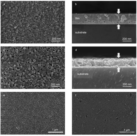
Fig.2 is the SEM images of as-deposited and PbO-PbI2hybrid thin films with and without application of ultrasonic rinsing.The number of deposited cycles is 20.The top-view images of asdeposited films with ultrasonic rinsing were depicted in Fig.2a.As indicated in which,as-deposited films were smooth and covered the substrates completely.Grains with size smaller than 20 nm made up the as-deposited films.Fig.2c shows that after heat treating,grains size of the PbO-PbI2hybrid thin films became slightly bigger and scattered voids among adjacent grains presented which caused by PbO grains growing up and Pb(OH)2decomposing,respectively.For the same reason,the cross section of PbO-PbI2hybrid films was full of pores which could be obviously observed via contrasting Fig.2(b,d).These pores acted as transport tunnel of CH3NH3I gas in vapor-process,therefore pores were beneficial for vapor reaction proceeding.
In ultrasonic-assisted SILAR process,ultrasonic rinsing is of great importance for obtaining uniform films.Fig.2(e,f)shows the surface of PbO-PbI2hybrid thin films with and without application of ultrasonic rinsing.For PbO-PbI2hybrid thin films without ultrasonic rinsing,certain amount of large grains and film peeling off from substrates were observed clearly while smooth surface and full surface coverage were obtained after ultrasonic rinsing.In every SILAR cycle,lead nitrate complex ETA reacted with sodium iodide.And the precipitates,with different adsorptive attraction and particles size,attached on film surface.The function of ultrasonic rinsing is primarily to remove loose and large grains of film.So PbO-PbI2hybrid thin films obtained from ultrasonicassisted SILAR are more smooth and compact.
Fig.3 shows the relationship between PbO-PbI2hybrid thin films thickness and the number of ultrasonic-assisted SILAR cycles.Alinear dependence on the number of cycles was observed which was consistent with traditional SILAR technique results.However,an amazing growth rate of average 13 nm per cycle was obtained which was significantly higher than traditional SILAR technique.22With this high growth rate,PbO-PbI2hybrid thin films with 656 nm thickness could be achieved only after 50 deposition cycles.The morphology characterization of different cycles is similar.

Fig.2 Top-view SEM images of(a)as-deposited films,(b)cross section of(a),(c)PbO-PbI2hybrid films,(d)cross section of(c), (e)lower resolution image of(c),and(f)hybrid films without ultrasonic rinsing

Fig.3 cross section SEM images of PbO-PbI2hybrid films with (a)10 cycles and(b)50 cycles
3.3 Morphology characterization of CH3NH3PbI3thin films
Fig.4a shows the top-view SEM images of CH3NH3PbI3thin films.It was clearly that the CH3NH3PbI3thin films had full surface coverage on the substrates.Detail surface morphology is shown in Fig.4b which is the high resolution of Fig.4a.The CH3NH3PbI3grain size is up to 400-500 nm which is one order of magnitude bigger than that of PbO-PbI2hybrid films.The relative high temperature of vapor process promotes rearrangement and growing up of small grain in PbO-PbI2hybrid films so that grain size of CH3NH3PbI3thin films increases up to sub-micrometers.The smooth surface of PbO-PbI2hybrid films resulted in relatively small roughness of CH3NH3PbI3films.All the characteristics of CH3NH3PbI3thin films suggested its promising application in photovoltaic devices.
In vapor process,the reaction temperature has a giant effect on CH3NH3PbI3thin film quality.As shown in Fig.4d,the CH3NH3PbI3thin films fabricating at 150°C pelt off glass sub-strate so that a number of cracks between film and substrate appeared.However,impact cross section was achieved when the reaction temperature reduced to 110°C.The reaction rate between PbO-PbI2hybrid films and CH3NH3I vapor is crucial for fabricating high quality CH3NH3PbI3thin films.150°C temperature results in very fast reacting which produces large internal stress in CH3NH3PbI3thin films.So CH3NH3PbI3thin films peel off from substrates easily and the quality of CH3NH3PbI3thin films intensively deteriorates.

Fig.4 (a)Top-view SEM images of CH3NH3PbI3thin films,(b)high resolution of(a),cross section SEM images of CH3NH3PbI3thin films at(c)110°C and(d)150°C
The surface SEM images of CH3NH3PbI3thin films which prepared by different methods are shown in Fig.5.Details about CH3NH3PbI3perovskite film fabrication process including twostep solution method and vapor-assisted solution process could be found elsewhere.11,13By contrast,it is observed that the ultrasonicassisted SILAR derived CH3NH3PbI3thin films have uniform and compact morphology without any voids and cracks.However,the CH3NH3PbI3perovskite films fabricated by the other two processes are full of voids and cracks between perovskite grains.The two-step solution method and vapor-assisted solution process are all based on PbI2films prepared by solution spin-coating process. The solution spin-coating based PbI2films exhibit big grains of a few hundred nanometers and larger voids among grains.13Hence, after the perovskite films formation,voids and cracks do not vanish completely,even the perovskite grains growing up. Compared to the conventional PbI2films prepared by solution spin-coating process,the PbO-PbI2hybrid films are composed by much smaller grains with a few tens of nanometers and cracks between grains.During the transformation from PbO-PbI2hybrid films to perovskite films,the crystalline grains rearrange and the cracks disappear.

Fig.5 Top-view SEM images of CH3NH3PbI3films fabricated by(a)two-step solution method,(b)vapor-assisted solution process,and (c)ultrasonic-assisted SILAR technique
3.4 Composition and crystallinity of thin films
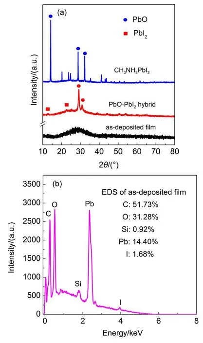
Fig.6 shows XRD pattern and EDS mapping of thin films.XRD pattern revealed the amorphous structure of as-deposited films caused by low operation temperature in ultrasonic-assisted SILAR process.Further identification of chemical compositions in asdeposited films was conducted by EDS analysis.Due to relatively thinfilms′thickness,the elements in glass substrates were also detected.Hydrogen element was neglected because of the limited detection of EDS.Atom ration of Pb and I was determined to be about 8.6:1 and this ration heavily deviated from 1:2 in pure PbI2. The departure of atom ration demonstrated the main component in as-deposited films was Pb(OH)2.Carbon element may come from ETAwhich would be removed in annealing procedure.
XRD pattern of PbO-PbI2hybrid films is shown in Fig.6(a).In XRD pattern,the diffraction peak of PbO could be clearly observed,but not for PbI2because of relative small amounts. Looking closely,there was a tiny signature peak at 12.69°corresponding to the(001)diffraction peak for PbI2.The presence of weak peak indicated PbI2phases in hybrid films.In XRD pattern of CH3NH3PbI3thin films,a series of main diffraction peaks at 14.16°,28.49°,and 31.85°which were assigned to(110),(220), (310)of the CH3NH3PbI3perovskite crystal respectively suggested formation of CH3NH3PbI3perovskite.The disappearance of PbO and PbI2characteristic peaks implied that CH3NH3PbI3perovskite films were high purity.Hence,the CH3NH3PbI3perovskite films fabricated by our method are high crystallinity and have few impurities.
3.5 Optical properties of thin films
Fig.7(a)shows the transmittance spectra in the wavelength range of 300 to 1000 nm of as-prepared films,PbO-PbI2hybrid films,and CH3NH3PbI3thin films.As contrast,optical property of glass slides without any films was included.The as-deposited films performed high transparency in the visible region and transmittance decreased slightly after annealing.However,for theCH3NH3PbI3thin films,high absorbance could be observed.In visible wavelength,CH3NH3PbI3thin films showed low transmittance below 10%.So the CH3NH3PbI3thin films were dark brown by naked eye.

Fig.6 (a)XRD patterns of films,(b)EDS of as-deposited films
The band gap of CH3NH3PbI3thin film was estimated by studying the relationship between adsorption coefficient(α)and photo energy(hv)as


Fig.7 (a)Transmittance spectra of thin films and glass slide substrate and(b)plot of(αhν)2-hν for CH3NH3PbI3films
In which,k is constant;the exponent m equals 1/2 for direct band gap materials and 2 for indirect gap materials.The absorption coefficient α was calculated after subtracting absorbance of glass substrate and neglecting reflectance at normal incidence.Fig.7(b) shows the plot of(αhν)2-hν for CH3NH3PbI3thin films.By elongating the linear part of the plot,the intercept of photo energy was determined as the band gap.For CH3NH3PbI3thin films,the band gap is 1.58 eV,which is well comparable with the band gap (1.51 eV)reported in previous article.23
3.6 Electrical properties of thin films

Fig.8 (a)Surface resistivity and(b)dielectric constant of CH3NH3PbI3perovskite films as a function of frequency
Fig.8(a)shows current-voltage(I-V)dependence of CH3NH3PbI3thin films.A remarkable behavior which can be easily spotted from I-V curve is the strongly non-Ohmic characteristics.Being repeatedly displayed at different applied voltages,the non-Ohmic properties are suggested to be attributed to ferroelectric response in CH3NH3PbI3.24The calculated surface resistivity value forprepared CH3NH3PbI3thin films by ignoring the nonlinear parts of the plot is about 1000 MΩ at room temperature.Interestingly, the surface resistivity value varies slightly with the applied voltage.A higher applied voltage generates a higher surface resistivity.Generally speaking,CH3NH3PbI3shows poor electrical conductivity.The conductivity type of CH3NH3PbI3thin films determined by Hall effect measurement is a p-type semiconductor with carrier concentration in the order of 1015cm-3.The carrier mobility is 5.8 cm2·V-1·s-1.The poor electrical conductivity could be related with low hole concentration.
The characteristic behavior of the frequency dependent of the dielectric constant of CH3NH3PbI3is also been detected as shown in Fig.8(b).The dielectric constant of CH3NH3PbI3thin films decreases from a low frequency value of about εr(100 Hz)=155 to the high frequency value in the order of tens.The high dielectric constant in low frequency implies that CH3NH3PbI3could be a candidate in energy devices.25
4 Conclusions
In summary,CH3NH3PbI3thin films were fabricated on glass substrates by reacting ultrasonic-assisted SILAR derived PbO-PbI2hybrid films with CH3NH3Ivapor at high temperature of 110°C. SEM,XRD,EDS,UV-Vis spectroscopy,surface resistivity,and dielectric constant test were performed to characterize the prepared CH3NH3PbI3thin films.The results showed that CH3NH3PbI3thin films derived from our approach exhibited full surface coverage,uniform structure with grain size up to 400 nm.The suitable band gap of 1.58 eV and electrical properties of high dielectric constant suggest that CH3NH3PbI3thin films prepared by our technique could be used in photovoltaic or other photoelectrical devices.Our method offers a relatively low-cost and convenient way to synthesize CH3NH3PbI3thin films with high quality for large-scale application.
(1)Noh,J.H.;Jeon,N.J.;Choi,Y.C.;Nazeeruddin,M.K.; Grätzel,M.;Seok,S.I.J.Mater.Chem.A2013,1,11842.doi: 10.1039/c3ta12681a
(2)Im,J.H.;Lee,C.R.;Lee,J.W.;Park,S.W.;Park,N.G. Nanoscale2011,3,4088.doi:10.1039/c1nr10867k
(3)Xing,G.C.;Mathews,N.;Sun,S.Y.;Lim,S.S.;Lam,Y.M.; Grätzel,M.;Mhaisalkar,S.;Sum,T.C.Science2013,342, 344.doi:10.1126/science.1243167
(4)Burschka,J.;Pellet,N.;Moon,S.J.;Humphry-Baker,R.;Gao, P.;Nazeeruddin,M.K.;Grätzel,M.Nature2013,499,316. doi:10.1038/nature12340
(5)Etgar,L.;Gao,P.;Xue,Z.S.;Peng,Q.;Chandiran,A.K.;Liu, B.;Nazeeruddin,M.K.;Grätzel,M.J.Am.Chem.Soc.2012,134,17396.doi:10.1021/ja307789s
(6)Kim,H.S.;Lee,J.W.;Yantara,N.;Boix,P.P.;Kulkarni,S.A.; Mhaisalkar,S.;Grätzel,M.;Park,N.G.Nano Lett.2013,13, 2412.doi:10.1021/nl400286w
(7)Chen,Q.;Zhou,H.P.;Song,T.B.;Luo,S.;Hong,Z.;Duan,H. S.;Dou,L.T.;Liu,Y.S.;Yang,Y.Nano Lett.2014,14,4158. doi:10.1021/nl501838y
(8)Jeng,J.Y.;Chen,K.C.;Chiang,T.Y.;Lin,P.Y.;Tsai,T.D.; Chang,Y.C.;Guo,T.F.;Chen,P.;Wen,T.C.;Hsu,Y.J.Adv. Mater.2014,26,4107.doi:10.1002/adma.v26.24
(9)Liu,M.Z.;Johnston,M.B.;Snaith,H.J.Nature2013,501, 395.doi:10.1038/nature12509
(10)Kim,H.S.;Lee,C.R.;Im,J.H.;Lee,K.B.;Moehl,T.; Marchioro,A.;Moon,S.J.;Humphry-Baker,R.;Yum,J.H.; Moser,J.E.;Grätzel,M.;Park,N.G.Sci.Rep.2012,2,591.
(11)Yella,A.;Heiniger,L.P.;Gao,P.;Nazeeruddin,M.K.;Grätzel, M.Nano Lett.2014,14,2591.doi:10.1021/nl500399m
(12)Mei,A.Y.;Li,X.;Liu,L.F.;Ku,Z.L.;Liu,T.F.;Rong,Y.G.; Xu,M.;Hu,M.;Chen,J.Z.;Yang,Y.;Grätzel,M.;Han,H.W. Science2014,345,295.doi:10.1126/science.1254763
(13)Chen,Q.;Zhou,H.P.;Hong,Z.;Luo,S.;Duan,H.S.;Wang,H. H.;Liu,Y.S.;Li,G.;Yang,Y.J.Am.Chem.Soc.2014,136, 622.doi:10.1021/ja411509g
(14)Kanniainen,T.;Lindroos,S.;Ihanus,J.;Leskela,M.J.Mater. Chem.1996,6,161.doi:10.1039/jm9960600161
(15)Kanniainen,T.;Lindroos,S.;Resch,R.;Leskela,M.; Friedbacher,G.;Grasserbauer,M.Mater.Res.Bull.2000,35, 1045.doi:10.1016/S0025-5408(00)00298-1
(16)Zhuge,F.W.;Li,X.M.;Gao,X.D.;Gan,X.Y;Zhou,F.L. Mater.Lett.2009,63,652.doi:10.1016/j.matlet.2008.12.010
(17)Zhang,Q.B.;Feng,Z.F.;Han,N.N.;Lin,L.L.;Zhou,J.Z.; Lin,Z.H.Acta Phys.-Chim.Sin.2010,26,2927.[张桥保,冯曾芳,韩楠楠,林玲玲,周剑章,林仲华.物理化学学报,2010,26,2927.]doi:10.3866/PKU.WHXB20101113
(18)Jambure,S.B.;Patil,S.J.;Deshpande,A.R.;Lokhande,C.D. Mater.Res.Bull.2014,49,420.doi:10.1016/j. materresbull.2013.09.007
(19)Sall,T.;Raidou,A.;Elfarrass,S.;Hartiti,B.;Mari,B.;Qachaou, A.;Fahoume,M.Opt.Quantum Electron2014,46,247.doi: 10.1007/s11082-013-9786-x
(20)Gao,X.D.;Li,X.M.;Yu,W.D.Thin Solid Films2004,468, 43.doi:10.1016/j.tsf.2004.04.005
(21)Shei,S.C.;Chang,S.J.;Lee,P.Y.J.Electrochem.Soc.2011,158,208.
(22)Su,Z.H.;Yan,C.;Sun,K.W.;Han,Z.L.;Liu,F.Y.;Liu,J.; Lai,Y.Q.;Li,J.;Liu,Y.X.Appl.Surf.Sci.2012,258, 7678.doi:10.1016/j.apsusc.2012.04.120
(23)Noh,J.H.;Im,S.H.;Heo,J.H.;Mandal,T.N.;Seok,S.I. Nano Lett.2013,13,1764.
(24)Stoumpos,C.C.;Malliakas,C.D.;Kanatzidis,M.G.Inorg. Chem.2013,52,9019.doi:10.1021/ic401215x
(25)Juarez-Perez,E.J.;Sanchez,R.S.;Badia,L.;Garcia-Belmonte, G.;Kang,Y.S.;Mora-Sero,I.;Bisquert,J.J.Phys.Chem.Lett.2014,5,2390.doi:10.1021/jz5011169
Optical and Electrical Properties of CH3NH3PbI3Perovskite Thin Films Transformed from PbO-PbI2Hybrid Films
DING Xu-Kun LI Xiao-Min*GAO Xiang-Dong ZHANG Shu-De HUANG Yu-Di LI Hao-Ran
(State Key Laboratory of High Performance Ceramics and Superfine Microstructures,Shanghai Institute of Ceramics, Chinese Academy of Sciences,Shanghai 200050,P.R.China)
Organic-inorganic halide perovskites have been shown to be outstanding photovoltaic materials, achieving remarkably high power conversion efficiency(15%)of sunlight to electricity within the past 4 years. The controllable synthesis of organic-inorganic halide perovskites is fundamental to their applications in photovoltaic devices.Here we explore a novel strategy to prepare a typical halide peroskite CH3NH3PbI3by transforming PbO-PbI2hybrid materials.CH3NH3PbI3thin films were deposited on glass substrates by reacting ultrasonic-assisted successive ionic layer adsorption and reaction(SILAR)-derived PbO-PbI2hybrid films with CH3NH3I vapor at 110°C.The microstructure and crystallinity of the films,together with the optical and electrical properties were characterized.Results show that CH3NH3PbI3thin films possess perovskite crystal structure and uniform surface morphology with grain size up to 400 nm.In the visible band,CH3NH3PbI3thin films showed low transmittance(below 10%),with a band gap of 1.58 eV.The surface resistivity of CH3NH3PbI3thin films was as high as 1000 MΩ,indicating the dielectric nature of obtained CH3NH3PbI3films,with a dielectric constant of εr(100 Hz)=155 on low frequency.The current work opens an effective route toward high quality organicinorganic halide perovskite films with good crystallinity and optical properties,which make them suitable for application in photovoltaic devices,and other optical and electrical applications.
O649
10.3866/PKU.WHXB201501201www.whxb.pku.edu.cn
Received:November 13,2014;Revised:January 19,2015;Published on Web:January 20,2015.
∗Corresponding author.Email:lixm@mail.sic.ac.cn;Tel:+86-21-52412554.
The project was supported by the National Natural Science Foundation of China(50502038,10576036).
国家自然科学基金(50502038,10576036)资助项目
