A reconfigurable active-Gm-RC filter for multistandard wireless receivers①
2015-04-17FanXiangning樊祥宁
Fan Xiangning (樊祥宁)
(Institute of RF-&OE-ICs, School of Information Science and Engineering, Southeast University, Nanjing 210096, P.R.China)
A reconfigurable active-Gm-RC filter for multistandard wireless receivers①
Fan Xiangning (樊祥宁)②
(Institute of RF-&OE-ICs, School of Information Science and Engineering, Southeast University, Nanjing 210096, P.R.China)
A 4th-order low-pass filter (LPF) based on active-Gm-RC structure for multi-standard system application is presented in this paper. The performances of LPF are controlled by a 1-bit control-voltage, and the cut-off frequency, channel selectivity, and linearity of the proposed filter can be reconfigured accordingly. In order to improve the accuracy of the cut-off frequency, a binary-weighted switched-capacitor array is employed as the auto-tuning circuits to calibrate the RC-time constant. Fabricated in TSMC 0.18μm RF CMOS process, the proposed LPF achieves a measured cut-off frequency of 1.95 and 12.3MHz for WCDMA and GPS/Galileo application with a bandwidth deviation less than 4%. The measured 1dB compression points are -3.0dBm and -5.1dBm respectively for different modes. The core circuit of LPF consumes 1mW and 1.6mW for WCDMA and GPS/Galileo respectively. And the proposed LPF occupies an area of 0.78mm2.
low pass filter (LPF), multi-standard, active-Gm-RC, auto-tuning, WCDMA, GPS, Galileo, reconfigurability
0 Introduction
Recently, as the emerging of various wireless communications standards for commercial and personal communication, there is a strong trend in integrating multi-functions in one receiver with very low cost and power consumption[1]. One single receiver with digitally-controllable re-configurability is a good solution to provide multi-standard communication capability[2,3]. As the channel bandwidth of different communication standards varies a lot, it is necessary to reconfigurate the cut-off frequency of the low pass filter (LPF) in the front end of the receiver in terms of channel selection and interference attenuation[4-6]. In this paper, WCDMA and GPS/Galileo are included in a direct-conversion receiver, which are intended to provide seamless indoor/outdoor navigation and communication capability[7,8]. This paper focuses on the design and measurement of a LPF with reconfigurable characteristics such as cut-off frequency, power consumption, linearity, etc. The proposed LPF can provide different signal channel selectivity for multiple communication standards.
In recent years, some attempts at a reconfigurable
filter have been made for multi-mode applications[9-14]. A fully reconfigurable filter architecture that employs sub-blocker arrays and a digital assistant was proved to be the best candidate to implement a baseband filter for SDR applications[4]. However,there are lots of room for the performance improvement of filters’ reconfigurability, chip area and power consumption, etc.
Typically a continuous analog filter is cascade combination of several 1stand 2ndorder filtering cells[15]. The 2ndorder cell is also called biquad. Active RC integrators are commonly used as the 1storder cell to generate 1 pole in the filter’s transfer function[15]. And active RC biquad, Gm-C biquad, and MOSFET-C biquad are widely used to generate a pair of conjugated poles[16]. Filters based on active RC structure have high linearity and large dynamic range and are insensitive to parasitic parameters and widely used in reconfigurable low pass filters to achieve high linearity and accurate cut-off frequency. However, as for some communication standards with channel bandwidth larger than 10MHz, the required unit gain bandwidth of the OPA in the active RC filter is very large, which consequently causes much higher power consumption[6]. Gm-C structure[11,12]is suitable for filters to realize high bandwidth filtering and is easy for the tuning of cut-off frequency. However, it has limited dynamic range and poor linearity. MOSFET-C structure[12]enables transistors operating in linear region to realize and voltage-controlled variable resistors and to replace conventional resistors. This is a solution for integrated high precision monolithic continuous time filters, but there exists serious nonlinearity problem in MOS resistor.
Considering both linearity and power consumption, an active-Gm-RC structure[16-18], a combination of the active-RC structure and Gm-C structure, is employed in this paper. In order to obtain sufficient out of band rejection, the filter employs a 4th-order Butterworth topology.
Due to process variation, changing of operation environment (such as power supply voltage, temperature, etc.) and device aging, the transfer function of filters will also change. So an automatic tuning system is needed to adjust the device parameters to calibrate the transfer function to the designed value[15]. This paper uses indirect frequency tuning program with capacitor array to calibrate the non- ideality of the cut-off frequency of the filter.
1 The reconfigurable active-Gm-RC biquad
An active-Gm-RC structure has the advantage of very low power consumption due to the small required unit-gain-frequency (ωu) of the OTA[16]. To achieve the reconfigurability of the cut-off frequency, a reconfigurable 2ndorder low pass active-Gm-RC biquad in its single-ended fashion is shown in Fig.1. This biquad consists of a reconfigurable OTA that can be configured to different ωμ, two resistor-arrays (R1and R2) and one capacitor array (C1) that can be reconfigured according to the required pole frequency and Q factor.
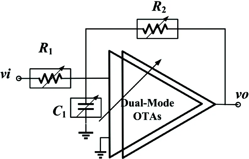
Fig.1 The dual-mode active-Gm-RC biquad
As discussed in Ref.[18], the transfer function of a biquad can be derived as
(1)
where ωμis the unity-gain-bandwidth of the OTA.
From Eq.(1), the DC gain ADC, pole frequency f0(i.e., the cut-off frequency fLP) and quality factor QLPof the biquad can be calculated as
(2)
The relationship between the cut-off frequency fLPand the ωuof the OPA is
ωu=2πQLP(1+ADC)fLP
(3)
During reconfiguration of the LPF, the pole frequency of the biquad is reconfigured while the quality factor and DC-gain of the biquad are kept constant. For example, when the unit-gain-frequency of the reconfigurable OTA is increased by a ratio K, R1and R2should decrease to the 1/K of their original value, by which the low pass biquad’s pole frequency ωKis changed while the quality factor Q, and DC-gain ADCare kept constant, as derived in Eqs(4-6).
(4)
(5)
(6)
This active-Gm-RC cell exhibits the following features that make it preferable for the implementation of baseband filter of wireless multi-standard applications.
1) Low power consumption and high linearity

2) Power-scalable reconfigurability
The cut-off frequency along with the power consumption of the filter is desired to be adjustable according to the requirement of different communication standards[6]. The power consumption of the flexible LPF is needed to be proportional to the level of performance. Programmability of the power consumption for the analog front-end allows minimizing the energy consumption in each functioning mode. As discussed in Eqs(4-6), the cut-off frequency of the active-Gm-RC filter can achieve flexible reconfigurability with programmable passive component arrays and OPAs arrays. The power consumption is also reconfigured by changing the current of the OPAs. Furthermore, to achieve a more accurate frequency response, a tuning system is necessary to prevent suffering from the spread of fabrication process.
2 Dual-mode active Gm-RC LPF design
The LPF proposed in this paper is designed for a dual mode communication receiver for WCDMA and GPS/Galileo, which is intended for wireless mobile communication and seamless indoor/outdoor navigation capability. This section will talk about the detail design of the main circuit and the RC-constant tuning circuits of the proposed LPF.
2.1 Main circuits
Table 1 summarizes the frequency response characteristics for each cell for the synthesis of a 4th-order Butterworth filter transfer function. The key feature of this structure is the use of low ωuOPAs. In fact, the ratio fu/fLPfor both cells is lower than 3, which reduces the OPA power consumption strongly. The above value has been optimized in order to minimize the power consumption according to the specification set (noise, linearity, transfer function) of all the device sizes with the key target of the power minimization.
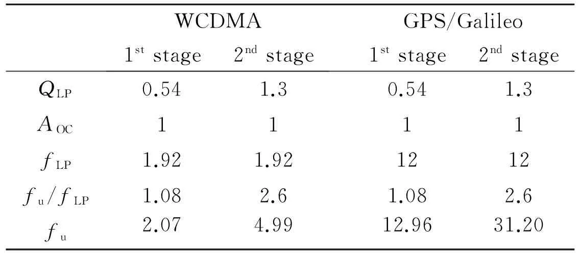
Table 1 Parameters of the proposed LPF required by WCDMA and GPS/Galileo
Fig.2 shows the architecture of the 4th-order WCDMA and GPS/Galileo reconfigurable filter. It is a cascade of 2 active-Gm-RC biquad cells. The challenge of this design is the realization of an efficient dual-mode filter in terms of power and area occupation, while guaranteeing the large linear range required by the WCDMA and GPS/Galileo standards. The filter can be reconfigured in order to adjust the filter bandwidth to the selected standard (1.92MHz and 12MHz for WCDMA and GPS/Galileo standards, respectively), by a single standard-selection (SS) bit that controls the values of the resistors. In addition, for the WCDMA case the power consumption is reduced by controlling the input stage device MOS sizes and its current levels. For both standards, the capacitors are grounded in order to be also active for the common-mode signal; otherwise a resonance at high frequency for input common-mode signals would be present.

Fig.2 Architecture of the 4th-order LPF
Fig.3 shows the fully-differential 2-stage OPA implementation in CMOS technology of the proposed LPF. The input transconductance stage consists of a pair of reconfigurable differential transistors M1 and M2. By controlling switch SS, gmof OPA is configured according to the requirement of the unit gain bandwidth. M7~9 provide 3 reconfigurable current sources for OPA, which improves the power efficiency of LPF. The common-mode feedback circuit is implemented with an additional differential pair. A Miller compensation scheme (RCand CC) is used to stabilize OPA[15].
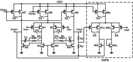
Fig.3 Schematic of the OPA
From Eqs(4-6), the cell’s DC gain K is determined by resistor ratio and is less affected by process, because resistor matching can be well done on the same chip. Quality factor Q is determined by R2/R1, gm1, R2and C1/CC. And both R2/R1and C1/CCare stable, so the constant transconductance technology which makes gm=1/Rrefis applied to improve the stability of Q. Fig.4 shows the constant gm circuit and it also provides bias to OPA. So the cell’s pole frequency f0and quality factor Q can be derived as:
(7)
From Eq.(7), the filter’s frequency response and quality factor is only related to the RC time constant. Similarly, when the operating mode changes, the constant gmcircuit should also be able to be reconfigured to maintain gm=1/Rref.
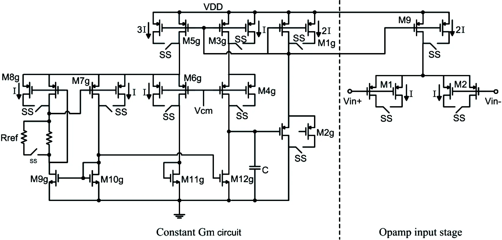
Fig.4 Constant Gm circuit
2.2 Tuning circuit design
The proposed filter can be reconfigured to adjust the bandwidth to the selected communication standard (1.92MHz and 12.28MHz for WCDMA and GPS/Galileo, respectively), which is realized by controlling a single standard-selection (SS) bit. The main factor to change the filter pole frequency f0is the RC time constant deviation[18]. The RC time constant auto-tuning circuit in Fig.5 mainly consists of an error amplifier, comparator, charging loop and digital module. This circuit firstly compares its RC time constant with a precise external clock period, and generates a 5-bits code. When calibration ends, this 5-bits code is sent to arrange the binary-weighted capacitors array. The resistor Rrefand capacitor array Cbankshould be respectively matched with the ones in the filter’s main circuit in order to undergo the same process. Finally the RC constant is equal or as close as possible to the default value, and then the accuracy of filter bandwidth will be ensured.

Fig.5 RC time constant auto-tuning circuit
Because of the negative feedback formed by the error amplifier and transistor M3, the voltages of the amplifier’s positive and negative input are approximately equal, i.e., Vs=Vref. So current ICflowing through reference resistor Rrefis
(8)
This current is copied to the capacitor branch by the current mirror and charges on the capacitors array when the charge clock comes. Suppose the charge clock is △t in one tuning period, after charging, Vcis
(9)
where Cnomis the capacitor array value before tuning. The comparator compares charge voltage Vcwith reference voltage Vcom. If Vcis larger (smaller) than Vcom, the control word produced by the digital unit pluses (minuses) “1”, i.e., the capacitors array value increases (decreases) a capacitor unit. Then another new tuning period will begin. Fig.6 describes the tuning period.

Fig.6 One tuning period
At last, Vcis equal to Vcomin theory, and then
(10)
It is assumed that both resistor and transconductance are ideal, and all the deviation of time constant is caused by the capacitor. So the binary-weighted switch capacitor array which is shown in Fig.7 is adopted. The capacitor array consists of a set of fixed capacitor and a set of N bits binary-weighted capacitors. The fixed capacitor is made up of Cfix1, Cfix2and some switches. In the N bits binary-weighted capacitors, C0is the minimum capacitor, i.e. basic unit of capacitor. The switches are controlled by the N bits digital code which is outputted by the tuning circuit. The capacitor array can also correspondingly switch according to the external control signal. Considering MOS switches will also contribute some parasitic capacitance, the switch connected to XC0consists of X MOS switches in parallel to achieve the same capacitance ratio. The total capacitor array value is[18]:
(11)
where n=0…(2N-1). Take into account the process variation as ξ%,

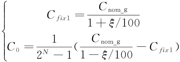
(12)
where Cnom_wand Cnom_gis the designed capacitor array value in WCDMA and GPS/Galileo respectively.
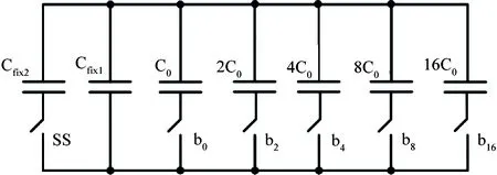
Fig.7 Binary-weighted switch capacitors array
In order to ensure the tuning circuit to work, 4 clocks are required, respectively for discharging, charging, collecting the compared result and outputting the control code. So a divided clock generation module is needed to generate 4 clocks in the digital tuning module. In addition, there also needs a register to capture the result of the comparator, a decoder to decode the result, an adder to generate the next 5-bits control code value and a register to output the final 5-bits control code. In order to allow power saving, the calibration circuit can be switched off after tuning. The internal block diagram in the digital tuning module is shown in Fig.8.

Fig.8 The internal block diagram in the digital tuning module
3 Measurement results
The proposed active-Gm-RC filter is fabricated in TSMC 0.18μm RF CMOS technology. Symmetrical structure and the common centered technique are employed in the layout designing to reduce mismatches and nonlinearities of the filter. And the digital parts of the filter are well isolated from the analog part to prevent the disturbance of the noise from digital circuits. The chip die of the filter occupies a silicon area of 0.78mm2. The right side of the chip is the analog circuits, including two biquads and a buffer. The left part is the tuning circuit, where the digital circuit is located in the upper left corner of the chip, and as far as possible from the other. Both power supply and ground of analog and digital circuits are separated, and digital circuit is surrounded by guard-ring to reduce noise coupling.
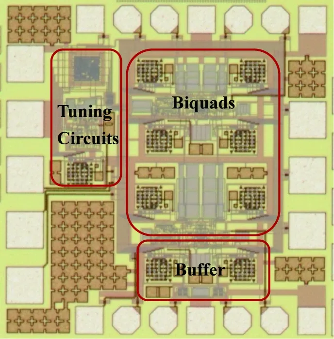
Fig.9 Die-photograph of the proposed LPF
The amplitude-frequency characteristic curves are shown in Fig.10. Two -3dB bandwidths are achieved: 1.95MHz and 12.28MHz for WCDMA and GPS/Galileo, respectively. The out of band attenuation rate is about -78dB/decade.
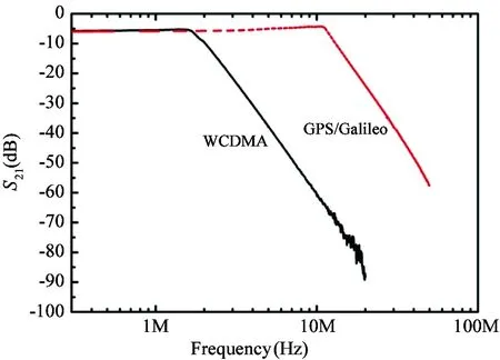
Fig.10 The amplitude-frequency characteristic curves
Fig.11 shows the 1dB compression point (1dBcp) for both modes. And the measured 1dBcp is respectively -3.0dBm for WCDMA and -5.1dBm for GPS/Galileo.

Fig.11 1dBcp for both modes
Table 2 summarizes the filter performance and comparison with other LPFs published resently. The comparison results shows that the proposed LPF exhibits an obvious advantage of low power consumption, high linearity and bandwidth reconfigurability, and is a good alternative for multi-standard applications.
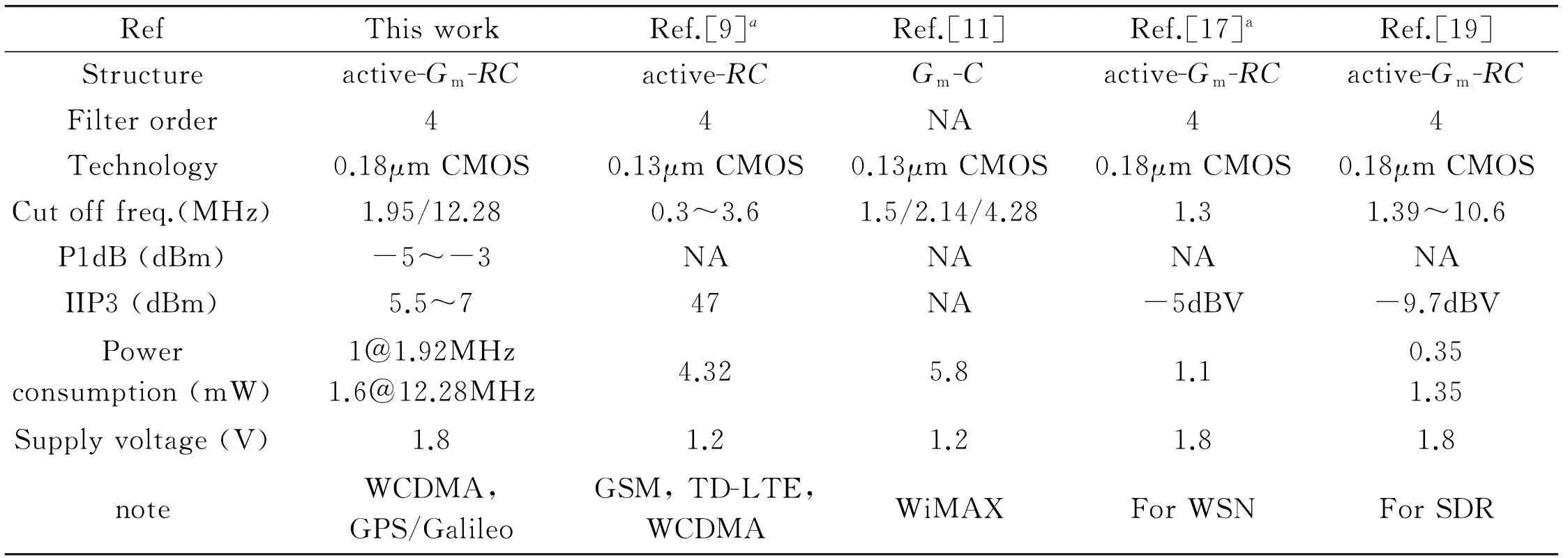
Table 2 Summary of the proposed LPF and the comparison with other resent publications
aSimulated results
4 Conclusion
This paper reports a 4th-order reconfigurable Butterworth low-pass filter for multi-mode of dual mode (WCDMA and GPS/Galileo) applications. Low power active-Gm-RC biquads are employed to achieve a 4thorder filtering transfer function. The RC time constant auto-tuning circuit is also designed to calibrate the frequency variation caused by process corner and temperature, by which the bandwidth error is less than 4%. The chip test results show that the reconfigurable filter exhibits flexible reconfigurability, very low power consumption and high linearity. The proposed LPF provides an excellent alternative for multi-mode multi-standard communications.
[ 1] Abidi A A. The path to the software-defined radio receiver. IEEE Journal of Solid-State Circuits, 2007, 42(5): 954-966
[ 2] Giannini V, Nuzzo P, Soens C, et al. A 2-mm20.1-5 GHz software-defined radio receiver in 45-nm digital CMOS. IEEE Journal of Solid-State Circuits, 2009, 44(12): 3486-3498
[ 3] Chen J M, Xu Y B, Ma L, et al. A dynamic programming algorithm for network selection in 3G/WLAN. High Technology Letters, 2013,19(4):364-370
[ 4] Brandolini M, Rossi P, Manstretta D, et al. Toward multistandard mobile terminals-fully integrated receivers requirements and architectures. IEEE Transactions on Microwave Theory and Techniques, 2005, 53(3):1026-1038
[ 5] D’Amico S, Giannini V, Baschirotto A. A 4th-order active-Gm-RC reconfigurable (UMTS/WLAN) filter. IEEE Journal of Solid-State Circuits, 2006, 41(7):
[ 6] Giannini V, Craninckx J, D’Amico S, et al. Flexible baseband analog circuits for software-defined radio front-ends. IEEE Journal of Solid-State Circuits, 2007, 42(7): 1501-1512
[ 7] Kuan B, Xiangning F, Wei L, et al. A wideband LNA employing gate-inductive-peaking and noise-canceling techniques in 0.18 μm CMOS. Journal of Semiconductors, 2012, 33(1): 015003
[ 8] Chen Y M, Jing Y K, Zhang L. Design of a programmable frequency divider in GPS frequency synthesizers. Chinese High Technology Letters, 2011, 21(4): 434-437 (In Chinese)
[ 9] Yongchang Y, Kefeng H, Lifang W, et al. A baseband LPF for GSM, TD-SCDMA and WCDMA multi-mode transmitters. Journal of Semiconductors, 2011, 32(2): 025003
[10] Lim J, Cho Y, Jung K, et al. A wide-band active-RC filter with a fast tuning scheme for wireless communication receivers. In: Proceedings of IEEE Custom Integrated Circuits Conference, California,USA, 2005. 637-640
[11] Xin C, Haigang Y, Tongqiang G, et al. A CMOS Gm-C complex filter with a reconfigurable center and cutoff frequencies in low-IF WiMAX receivers. Journal of Semiconductors, 2013, 34(7): 075004
[12] Kurahashi P, Hanumolu P K, Temes G C, et al. Design of low-voltage highly linear switched-R-MOSFET-C filters. IEEE Journal of Solid-State Circuits, 2007, 42(8):1699-1709
[13] Crombez P, Craninckx J, Wambacq P, et al. A 100-kHz to 20-MHz reconfigurable power-linearity optimized-biquad in 0.13-m CMOS. IEEE Transactions on Circuits and Systems II: Express Briefs, 2008, 55(3): 224-228
[14] Weiwei W, Xuegui C, Xiao W, et al. A 4th-order reconfigurable analog baseband filter for software-defined radio applications. Journal of Semiconductors, 2011, 32(4): 045008
[15] Chi Baoyong. Analog integrated Circuits and Systems, Tsinghua University Press, Beijing, 2012 (In Chinese)
[16] Junbo L, Xiangning F, Kuan B. A 4th-order active-Gm-RC low-pass filter with RC time constant auto-tuning for reconfigurable wireless receivers. In: Proceedings of 2012 IEEE 11th International Conference on Solid-State and Integrated Circuit Technology, Xi’an, China, 2012. 1-3
[17] Fan X N, Zhang L, Zhu C S. An active-Gm-RC structured CMOS analog filter with time constant auto-tuning. In: Proceeding of International Conference Wireless Communications Networking and Mobile Computing, Chengdu, China, 2010. 1-4
[18] Amico Stefano D’, Baschirotto A. Active-Gm-RC continuous-time biquadratic cells. Analog Integrated Circuits and Signal Processing, 2005, 45: 281-294
[19] Bao K, Fan X N, Wang Z G. A 0.18μm-CMOS low-power reconfigurable low pass filter for multi-standard receivers. In: Proceedings of International Conference on Advanced Technologies for Communications, Vietnam, 2013. 370-373
Fan Xiangning, born in 1964. He received the BS and MS degrees both from Nanjing University of Posts and Telecommunications in 1985 and 1988 respectively. From 1997, he became a part time Ph.D in National Communications Research Laboratory (NCRL), Southeast University and received the Ph.D degree in 2005. Since 1988, he works in Southeast University and now he is a Professor in Institute of RF-&-OE-ICs, School of Information Science and Engineering, Southeast University. Prof. Fan has finished more than 20 national projects and published over 100 papers. His current research interests include RF ICs, receiver design and signal processing of wireless systems.
10.3772/j.issn.1006-6748.2015.02.001
①Supported by the National Basic Research Program of China (No. 2010CB327404) and the Priority Academic Program Development of Jiangsu Higher Education Institutions.
②To whom correspondence should be addressed. E-mail: xnfan@seu.edu.cn Received on Apr. 9, 2014, Bao Kuan, Tang Li, Liu Junbo, Gu Chengjie
杂志排行
High Technology Letters的其它文章
- Improving wavelet reconstruction algorithm to achieve comprehensive application of thermal infrared remote sensing data from TM and MODIS①
- Security analysis of access control model in hybrid cloud based on security entropy①
- Multi-sensor federated unscented Kalman filtering algorithm in intermittent observations①
- MPLPK: A mobile path localization protocol based on key nodes①
- Research on suppress vibration of rotor misalignment with shear viscous damper①
- Design and development of real-time query platform for big data based on hadoop①
