DISCONTINUOUS GALERKIN TIME DOMAIN METHOD FOR SOI THIN-RIDGE WAVEGUIDE PROBLEM
2013-12-02GaoSiping高思平CaoQunsheng曹群生
Gao Siping(高思平),Cao Qunsheng(曹群生)
(College of Electronic and Information Engineering,Nanjing University of Aeronautics and Astronautics,Nanjing,210016,P.R.China)
INTRODUCTION
In the emerging area of silicon photonics,silicon-on-insulator(SOI)waveguides have attracted much attention because of their importance for many integrated photonic devices[1].Unlike common semiconductor waveguides like glass,polymer,and III-V,the SOI waveguides retain relatively large mode areas with large index of refraction contrast between the core and both the upper and the lower cladding layers.However,when operated in transverse-magnetic (TM)modes,this kind of shallow ridge waveguides[2]show strong evanescent fields and experience severe inherent lateral radiation leakage loss[3-4],which causes strong waveguide width dependence of the propagation loss[5].This strong width-dependent loss can limit usefulness of this SOI waveguide for traditional optic applications.Therefore,effective simulation methods are highly required for modeling SOI waveguide structure to acquire leakage loss minima.It is noted that many methods have been used to analyze SOI waveguide,including analytical mode matching technique[4,6-7]and numerical methods such as finite difference time-domain(FDTD)approach based on traditional Yee′s scheme[8]and the finite element method(FEM)using vector wave equation[3,9].However,these numerical methods suffer from low accuracy,low efficiency and complex boundary condition.
Therefore,a high-order three-dimensional(3-D) discontinuous Galerkin time domain(DGTD)method[10-11]is introduced and first applied to simulate thin shallow ridge structure.The DGTD method dates back to the utilization in the context of steady-state neutron transport[12]in 1973.In later works,it has also been used in other research fields such as acoustics,plasma physics,and photonics.Combined with Runge-Kutta scheme[13],the DGTD method shows promising results for hyperbolic systems.Recently,this method has been developed for dispersive media and the uniaxial perfectly matched layer(UPML)[14-15].Compared with FDTD and FEM methods,the DGTD method has shown obvious advantages including:(1)High-order accuracy in both spatial and temporal domain,(2)Unstructured meshes for conforming structure,(3)Discontinuous boundary easy treatment,(4)High efficient parallel implementation.In this paper,we adopt the DGTD method to analyze the structure of SOI ridge waveguide by utilizing mentioned advantages.
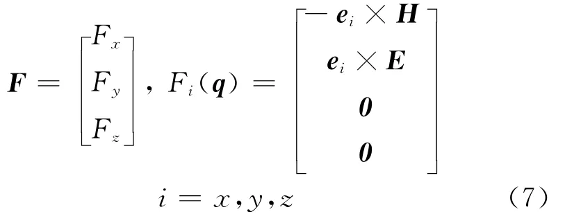
1 UNIFIED FORMULATION OF MAXWELL′S EQUATIONS WITH UPML
In order to normalize the Maxwell′s equations,the following unit-free variables are first used
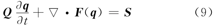
where the quantities with wavy lines″~″denote the non-normalized fields,c0and Z0= (μ0/ε0)1/2are the speed of light and wave impedance in free space,respectively,Eand Hthe electric field and the magnetic field vectors,and Lis the reference length relating to a given problem.
Then the fully 3-D time-dependent Maxwell′s equations in physical and UPML regions are considered,and the x-component variables are given as follows,where the auxiliary differential equation (ADE)technique[16]is used to handle the temporal convolution of the electromagnetic fields in the UPML region
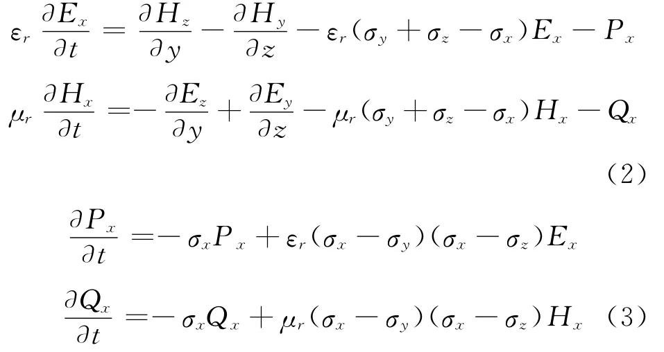
where Pand Qare the auxiliary polarization currents and Eq.(3)is ADE.The UPML lossσis usually set to get a polynomial profile[16]as
where r is the distance away from the interface between UPML and the physical solution domain,dthe thickness of UPML,andσmaxthe maximum loss in each direction.
The material property matrix is as follows
And the flux is
The source term which represent body forces(here the body forces are actually polarization currents)is
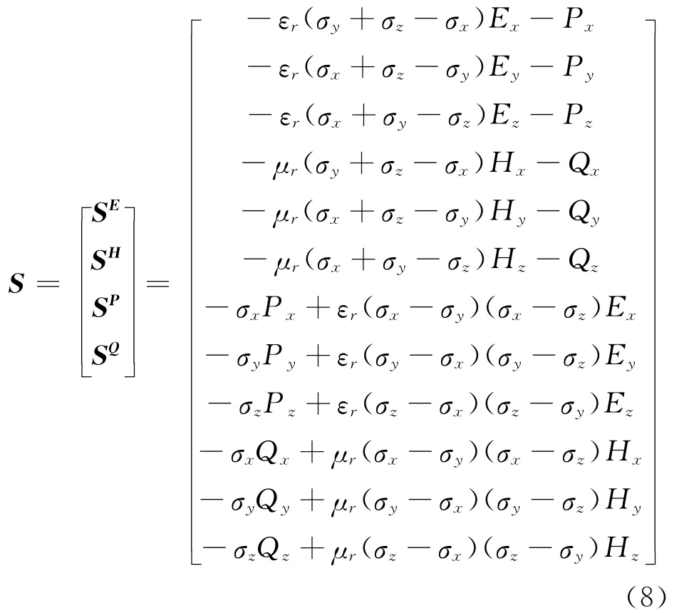
Then,it is easy to reformulate Eqs.(2-3)as the conservation law
2 DGTD METHOD
In order to solve Eq.(9)for general geometries problem,the physical domainΩ under consideration is tessellated into Knon-overlapping physical elementsΩk,k=1,…,K.Typically in 3-D cases,the domains are meshed by tetrahed-rons.For arbitrary elementΩk,the fields are then expanded in terms of interpolating Lagrange polynomials Li(r)
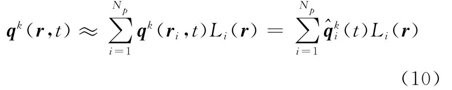
where r=(x,y,z)is the position vector,Npthe number of the coefficients that have been utilized as well as the number in the term in the local expansion.The relationship between Npand the polynomial expansion order Nis given as Np=(N+1)(N+2)(N+3)/6for tetrahedrons.The state vector^qkcontains the unknown fields′values to be solved.A carefully chosen set of interpolation nodes rilead to good numerical behavior[17].
The classic Galerkin method involves multiplying Eq.(9)with Li(r)and integrating over an elementΩk,which yields
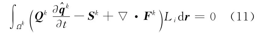
To facilitate the coupling with the neighbor elements,we integrate Eq.(11)by parts and obtain
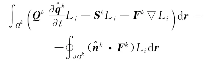
where^nk= (nx,ny,nz)is the outward-pointing unit vector normal to the contour of element k.
Then,after replacing the physical flux F(^qk)in the right-hand with the so-called numerical flux F*(^qk)and conducting a second integration by parts,we get
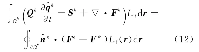
This is the strong formulation of Eq.(9).We can obtain the proper numerical flux by solving a local Riemann problem[10,14],which can make this formulation a stable and convergent scheme.One preferable choice is the well established pure upwind flux[18]as Eq.(13),which leads to strong damp of the unphysical modes
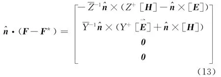
where[E]=E--E+and[H]=H--H+measure the jump in the field values across an interface,i.e.superscript″+″refers to the field values from the neighbor element while″-″the field values from the local element.For the possible difference of material properties between two elements,it is required to define local impedance and conductanceof the local impedance and conductance,respectively.Here the superscript kis dropped for clarity of notation.
Now,inserting the expansions Eq.(10)together with the numerical flux Eq.(13)into Eq.(12)and assuming parametersεr,μrandσiconstant in each element,we obtain the explicit expressions for the fields,which are ordinary differential equations(ODEs)
where Ek,Hk,Pk,and Qkare actually Np-vectors in elementΩk.And we have also defined the mass matrixΜk,the stiffness matrices∑kmalong the coordinate axes m,and the face mass matrix Fkwith respect to the element contour∂Ωkas below
To recover the solution of the above ODEs,a forth order,five-stage,low-storage Runge-Kutta scheme[13]is chosen,which is more efficient than the traditional methods like finite difference method and Newmark difference method.
3 NUMERICAL RESULTS AND DISCUSSIONS
In this section,we introduce a 3-D numerical scheme based on DGTD to analyze the lateral leakage of the TM-like mode in thin-ridge SOI straight waveguides.
3.1 Simulation geometry and parameter visualization experiment
Fig.1shows the cross-sectional geometry of the SOI thin-ridge waveguide,and the refractive indices nof each layer.This waveguide geometry consists of a core which has a thin ridge formed in a silicon slab,a lower cladding which is typically SiO2and an upper cladding which can be air or other dielectrics.Despite the high index contrast between the core and the cladding regions,this structure here can remain single-model at central frequency of 1.55μm wavelength according to Soref′s and Powell′s criteria[19-23].The main interest of this waveguide is the width dependence of its lateral leakage loss with TM-like mode excitation,where minima exists at a particular width wusually called the″magic width″[5].And this lateral leakage loss is not caused by any side-wall roughness but only the TM/transverse electric mode(TE)conversion at the ridge boundaries[4].
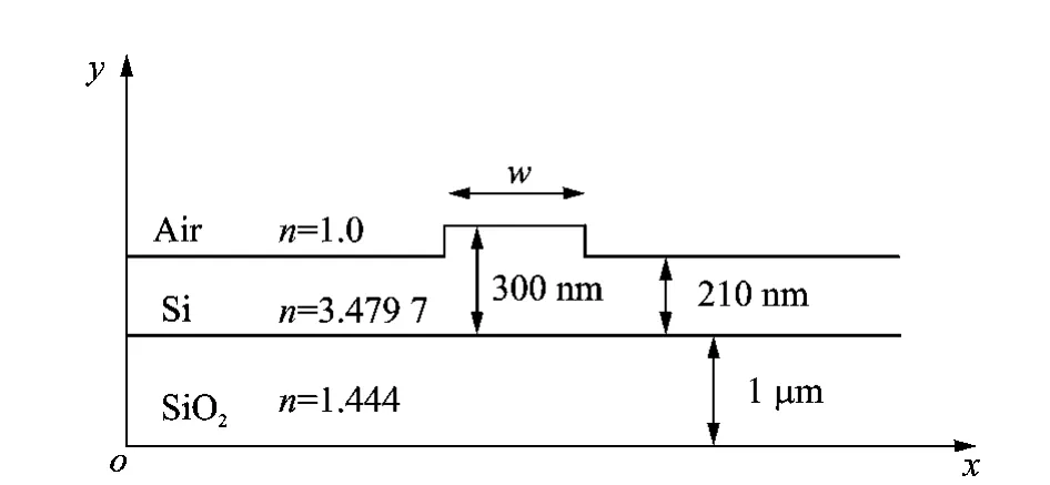
Fig.1 Cross section of SOI thin-ridge waveguide
In our simulation,as shown in Fig.2where TF means the total field and SF scattering field,the computational domain is 8μm×8μm in cross section and 9λ in the longitude,whereλ =1.55μm.And a 1μm-thick UPML is placed inside the computational domain,closed to the computational boundary.The boundary is considered as perfectly electric layer (PEC)withσmax=30 and m=3.Afterwards,we place a SOI thin-ridge waveguide in the middle of the computational domain,and set the center of the ridge as the origin of the coordinate system.The width of waveguide denoted as wvaries from 0.5to 1.6μm in 0.05 μm increment.
Modeling and meshing process is carried out by Gambit v2.4.As DGTD has a high-order accuracy,the average edge length of grids is usually less than 0.8λof the interesting central frequency to reduce the numerical dispersion[24].Therefore,an average edge length of 0.5μm is used and about 11 000vertexes and 60 000tetrahedrons are obtained.
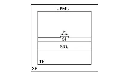
Fig.2 Cross section of computational domain (not to scale)
3.2 Source injection
The total field (TF)and scattering field(SF)technique[16]is employed to incorporate plane wave sources by simply changing the flux in Eq.(13)on the interface between TF and SF.As the TF is the caring fields,the SF domain and UPML is fully overlapped in this simulation.
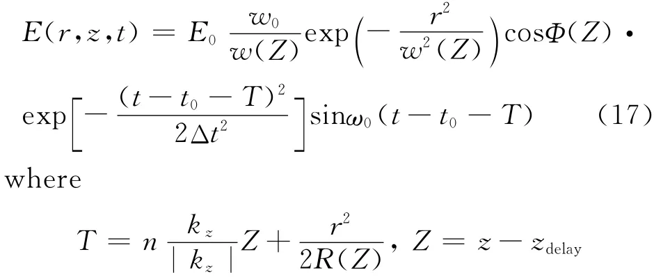
The introduced source is a pulsed source with 1.55μm wavelength,including both spatial and temporal distribution.In spatial domain,the source is a Gaussian beam imitating the laser in optical
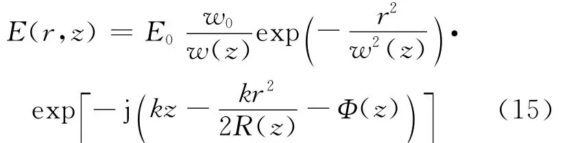
And consider the time dependence
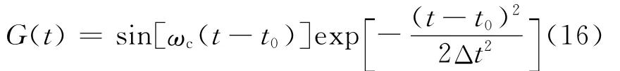
whereωcis the central frequency of 1.55 μm wavelength here,t0the location of the pulse peak in time domain andΔt half the pulse width.
After the combination and the normalization of Eqs.(15-16),the whole source is as below
3.3 Monitors and output
In order to recover the loss of SOI waveguides,two monitors in the longitude of the waveguide is placed to compare the incident power with the transmitted one.As the length of the waveguide is 9λ,both two monitors are 3λapart from the beginning and the end of the waveguide to let the evanescent waves decay,thus the effective length is 3λ. As the longitude of the waveguide is z-directional,the only power we care about is the time-averaged Poynting vector〈Sz〉as
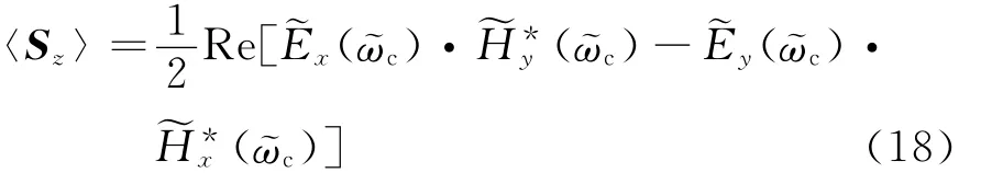
With the above information,the transmittance Tat central frequency is easily obtained via
And finally,the leakage loss of SOI thinridge waveguide can be evaluated by
3.4 Simulation results
Firstly,the simulation results of Excomponent of different basis function order Nis shown in Fig.3.They are all from the same modeling.From these curves,we can observe a good convergence of this method working on the SOI thin-ridge waveguide model.
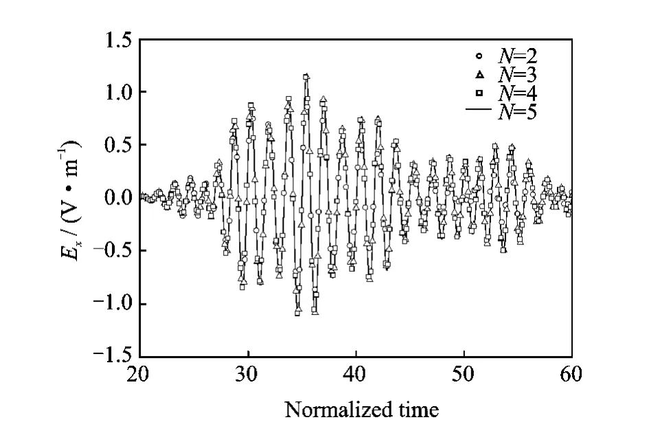
Fig.3 Exof different Nwith respect to time
Then,compared to analytical mode matching method,the L2-norm of the error of Exwith different orders Nis shown in Fig.4.It indicates that the error decreases exponentially with the increase of order N.Combining Fig.3and Fig.4,we can conclude that N=3is accurate enough for this problem.
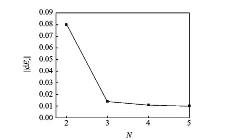
Fig.4 L2-norm of error of Exwith different orders N
Finally, the simulation results of SOI waveguides with different rib widths using DGTD are shown in Fig.5by the line with triangles.The other two results are represented by the line with squares carried out by Lumerical FDTD Solutions v7.5,and the solid line which is the result of mode matching method from Ref.[25],noted as MM.It is found that the result of DGTD agrees very well with that of the mode matching method.And competing with the commercial FDTD,the main advantages of DGTD method are as follows.
(1)The accuracy of the DGTD method dealing with SOI thin-ridge waveguide is better than that of the FDTD method,as the result of the former is closer to the analytical result.
(2)The efficiency of the DGTD method exceeds that of the FDTD method,as the average computation time of different modelings is about 5 h by the DGTD method compared to more than 6 h by the FDTD method.
In addition,it can be observed that for particular width such as 0.71μm and 1.43μm,the destructive interference of radiating TE waves result in low loss for TM-like guided mode.And it coincides with the width dependence of the leakage loss of such SOI waveguides.Hence,it can be concluded that the width-dependent leakage loss due to TM-TE conversion of straight SOI thin-ridge waveguides can be simulated efficiently and accurately by our DGTD scheme.
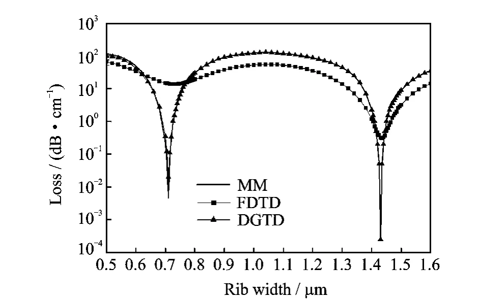
Fig.5 Simulation results between DGTD and FDTD
4 CONCLUSION
A high-order accuracy 3-D DGTD method is proposed for the calculation of the leakage loss of SOI thin-ridge waveguides.The method accurately predicts the strong width-dependent leakage loss of the TM-like mode in these waveguides,which proves it to be a more suitable scheme than the FDTD method for SOI thin-ridge waveguides or even more complex nano-optical devices.
[1] Jalali B,Fathpour S.Silicon photonics[J].Journal of Lightwave Technology,2006,24(12):4600-4615.
[2] Webster M A,Pafchek R M,Sukumaran G,et al.Low-loss quasi-planar ridge waveguides formed on thin silicon-on-insulator [J].Applied Physics Let-ters,2005,87(23):1-3.
[3] Nguyen T G,Tummidi R S,Koch T L,et al.Lateral leakage of TM-like mode in thin-ridge silicon-on-insulator bent waveguides and ring resonators[J].Optics Express,2010,18(7):7243-7252.
[4] Ogusu K.Optical strip waveguide:A detailed analysis including leaky modes[J].Journal of the Optical Society of America,1983,73(3):353-357.
[5] Webster M A,Pafchek R M,Mitchell A,et al.Width dependence of inherent TM-mode lateral leakage loss in silicon-on-insulator ridge waveguides[J].IEEE Photonics Technology Letters,2007,19(6):429-431.
[6] Sv Sudbo A.Improved formulation of the film mode matching method for mode field calculations in dielectric waveguides[J].Pure and Applied Optics,1994,3(3):381-388.
[7] Nguyen T G,Tummidi R S,Koch T L,et al.Rigorous modeling of lateral leakage loss in SOI thin-ridge waveguides and couplers[J].IEEE Photonics Technology Letters,2009,21(7):486-488.
[8] Yliniemi S,Aalto T,Heimala P,et al.Fabrication of photonic crystal waveguide elements on SOI[C]∥Integrated Optical Devices:Fabrication and Testing.Belgium:Giancarlo C R,2002:23-31.
[9] Srinivasan H,Bommalakunta B,Chamberlain A,et al.Finite element analysis and experimental verification of SOI waveguide bending loss[J].Microwave and Optical Technology Letters,2009,51(3):699-702.
[10]Hesthaven J S,Warburton T.Nodal discontinuous Galerkin methods:Algorithms,analysis,and applications[M].USA:Springer,2008.
[11]Liu Meilin,Liu Shaobin.High-order runge-Kutta discontinuous Galerkin finite element method for 2-d resonator problem[J].Transactions of Nanjing University of Aeronautics & Astronautics,2008,25(3):208-213.
[12]Reed W H,Hill T R.Triangular mesh methods for the neutron transport equation[R].LA-UR-73-479.Los Alamos:Scientific Laboratory,1973:73-79.
[13]Carpenter M H,Kennedy C A.Fourth-order 2N-storage Runge-Kutta schemes[R].NASA Technical Memorandum 109112,USA,1994.
[14]Lu T,Zhang P,Cai W.Discontinuous Galerkin methods for dispersive and lossy Maxwell′s equations and PML boundary conditions[J].Journal of Computational Physics,2004,200(2):549-580.
[15]Busch K,König M,Niegemann J.Discontinuous Galerkin methods in nanophotonics [J].Laser and Photonics Reviews,2011,5(6):773-809.
[16]Taflove A,Hagness S C.Computational electrodynamics: The finite-difference time-domain method[M].Third Edition.Boston:Artech House,2005.
[17]Warburton T.An explicit construction of interpolation nodes on the simplex[J].Journal of Engineering Mathematics,2006,56(3):247-262.
[18]Hesthaven J S, Warburton T. Nodal high-order methods on unstructured grids,I:Time-domain solution of Maxwell′s equations[J].Journal of Computational Physics,2002,181(1):186-221.
[19]Soref R A,Schmidtchen J,Petermann K.Large single-mode rib waveguides in GeSi-Si and Si-on-SiO2[J].IEEE Journal of Quantum Electronics,1991,27(8):1971-1974.
[20]Rickman A G,Reed G T,Namavar F.Silicon-on-insulator optical rib waveguide loss and mode characteristics[J].Journal of Lightwave Technology,1994,12(10):1771-1776.
[21]Pogossian S P,Vescan L,Vonsovici A.The singlemode condition for semiconductor rib waveguides with large cross section [J].Journal of Lightwave Technology,1998,16(10):1851-1853.
[22]Powell O.Single-mode condition for silicon rib waveguides[J].Journal of Lightwave Technology,2002,20(10):1851-1855.
[23]Lousteau J,Furniss D,Seddon A B,et al.The single-mode condition for silicon-on-insulator optical rib waveguides with large cross section [J].Journal of Lightwave Technology,2004,22(8):1923-1929.
[24]Hesthaven J S,Warburton T.High-order accurate methods for time-domain electromagnetics [J].CMES-Computer Modeling in Engineering and Sciences,2004,5(5):395-407.
[25]Tummidi R S,Nguyen T,Mitchell A,et al.Anomalous losses in curved waveguides and directional couplers at″magic widths″[C]∥21st Annual Meeting of the IEEE Lasers and Electro-Optics Society.Newport Beach,CA:IEEE,2008:521-522.
杂志排行

Transactions of Nanjing University of Aeronautics and Astronautics的其它文章
- FLEXURAL CAPACITY OF RC BEAM STRENGTHENED WITH PRESTRESSED C/AFRP SHEETS
- MINIMUM ATTRIBUTE CO-REDUCTION ALGORITHM BASED ON MULTILEVEL EVOLUTIONARY TREE WITH SELF-ADAPTIVE SUBPOPULATIONS
- OUTPUT MAXIMIZATION CONTROL FOR VSCF WIND ENERGY CONVERSION SYSTEM USING EXTREMUM CONTROL STRATEGY
- ACTIVE VIBRATION CONTROL OF TWO-BEAM STRUCTURES
- IMPROVED DOPPLER WARPING METHOD FOR AIRBORNE RADAR WITH NON-SIDELOOKING ARRAY
- MULTI-OBJECTIVE PROGRAMMING FOR AIRPORT GATE REASSIGNMENT