A novel topology with controllable wideband baseband impedance for power amplifiers∗
2024-03-01YaoYAOZhijiangDAIMingyuLI
Yao YAO ,Zhijiang DAI ,Mingyu LI
1School of Intelligent Technology and Engineering,Chongqing University of Science and Technology, Chongqing 400065, China
2School of Microelectronics and Communication Engineering, Chongqing University, Chongqing 400065, China
Abstract: This paper presents a novel topology to control the baseband impedance of a power amplifier (PA) to avoid performance deterioration in concurrent dual-band mode.This topology can avoid pure resonance of capacitors and inductors LC,which leads to a high impedance at some frequency points.Consequently,it can be applied to transmitters that are excited by broadband signals.In particular,by adjusting the circuit parameters and increasing stages,the impedance of the key frequency bands can be flexibly controlled.A PA is designed to support this design idea.Its saturated output power is around 46.7 dBm,and the drain efficiency is >68.2% (1.8–2.3 GHz).Under concurrent two-tone excitation,the drain efficiency reaches around 40% even under 5.5 dB back-offpower with the tone spacing from 10 MHz to 500 MHz.These results demonstrate that the proposed topology is capable of controlling wideband baseband impedance.
Key words: Baseband impedance;Concurrent dual-band;Power amplifier
1 Introduction
With the development of mobile communication,the bandwidth of the transmitted signal must be increased to improve the amount of information transmitted per unit time,such as the reported broadband and dual-band power amplifiers(PAs) (Liu et al.,2020;Kilinc et al.,2022;Latha and Rawat,2022;Li M et al.,2022;Sheikhi and Hemesi,2022).This requires that PAs can transmit broadband signals,and because the signal’s instantaneous bandwidth may exceed 400 MHz,new challenges have emerged in the design of PAs.Efficiency and linearity would be the key indicators(Li C et al.,2019;Feng et al.,2022;Cui et al.,2023).Because of the influence of the transistor’s nonlinear capacitance and nonlinear operating state,the baseband signal will be generated under multi-tone/broadband signal excitation.Conversely,the baseband signal will act on the transistor,which influences the memory effect and produces new modulation components.
The effect of baseband impedance was verified by adding different inductors and capacitors in the bias network,and good linear results were obtained by choosing an appropriate bias network in Brinkhoffand Parker (2003) and Brinkhoffet al.(2003).In the dual-band concurrent scenario,Chen et al.(2013) conducted in-depth research on overdrive effects.Nunes et al.(2018) showed that the baseband impedance of the output is the dominant factor in efficiency degradation.Barros et al.(2019)further showed that both input and output baseband impedances impact the PA performance.As presented in Nunes et al.(2018),efficiency degradation can reach 18%.
Previous studies have shown that the baseband impedance significantly impacts PA performance.The critical point was to avoid resonance in the baseband frequency band,where a high impedance will be presented at the current source plane.The baseband impedance was controlled by carefully designing the bias network in Nunes et al.(2018)and Barros et al.(2019).Although Zhu et al.(2017)proposed an in-package output impedance matching topology,it supports 395 MHz instantaneous bandwidth,and the output matching network needs to be carefully designed to prevent resonance.
When the baseband frequency is close to the operating frequency band,it is difficult to control flexibly,because capacitors need to be added in the power supply network in traditional baseband impedance control methods.However,there is a certain physical distance from the package of the transistor to the position of the filter capacitor,so it is difficult to obtain a low baseband impedance in a wide frequency band.In addition,the direct current (DC) bias capacitors may cause resonance,which results in high impedance at some frequency points.Therefore,in this paper we propose a novel topology to control baseband impedance covering the 10–500 MHz band,which can prevent PA performance deterioration under concurrent dual-band mode.
2 Analysis of the proposed topology
2.1 Analysis of an LC resonant network
It is well known that the expression of two parallel impedances(ZA=RA+jXA,ZB=RB+jXB)can be written as
IfRA=0 andRB=0,thenZAB →∞whenXA=-XB.
Furthermore,the input impedance function of a pureLCnetwork can be expressed as(Wing,2008)
wherei=0,j=1 ori=1,j=0.Kis a constant,andωm(m=1,2,...) are the poles or zeros of reactance function.There are two conclusions: (1) the reactance function of anLCimpedance function has a non-negative slope for allω;(2) the poles and zeros of anLCimpedance(admittance)function alternate on the jω-axis.This means that if the baseband impedance is controlled only through the bias branch with a pureLCnetwork,theLCimpedance function will circle around the edge of the Smith chart.In other words,controlling the baseband impedance with a small value in a broad bandwidth would be difficult.If it can be realized,it needs to depend on the parasitic resistance ofLorC.Therefore,it is necessary to propose a topology that can accurately control baseband impedance.
2.2 Proposed topology
A topology is proposed for avoiding the resonance mentioned above,as shown in Fig.1.The baseband impedance control unit (BICU) is connected in parallel with the input/output matching network,and each unit is composed of a microstrip transmission line (TL),a radio frequency (RF) capacitorCRF,a resistorRbb,and a low-frequency capacitorCSR.The primary function of RF capacitorCRFis to short the RF signal and reduce the loss of the fundamental signal in the BICU.The function ofCSRis to form seriesLCresonance with the circuit between pointsAandCi,orBandDj(as marked in Fig.1)and to reduce the baseband impedance.TheRbbfunction is introduced to avoid pureLCresonance among the BICUs.To control the baseband impedance in a wideband,four BICUs are shunted in the input and output matching networks.
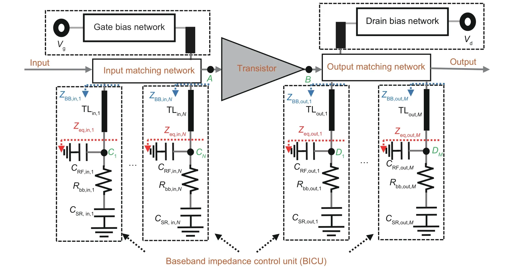
Fig.1 The proposed topology to control baseband impedance (Zeq,in,i=1/(jωCbb,in,i)+Req,in,i, Zeq,out,j=1/(jωCbb,out,j)+Req,out,j)
In this way,the impedance of each BICU can be written as
whereCbb,iandReq,iare the equivalent capacitance and resistance of theithBICU at pointC(D),and the impedance function can be written as
To intuitively describe the circuit characteristics of the proposed topology,the BICU parameters are assigned to observe how the overall equivalent impedance changes.First,several parameters are determined: the transmission line’s characteristic impedance is 77 Ω and the electrical length is 90◦at 2.2 GHz.CRFis a 10 pF capacitor of the Murata GRM series.CSRvalues of the three BICUs are 18,35,and 70 pF.ThenZBB,packagechange could be observed under different values ofRbb(Rbb={3,5,8,12}Ω).ZBB,ivalues of the three BICUs are shown in Fig.2a,and the impedance curves of the three cases are shown in Fig.2b.It can be seen from Fig.2 that the selection ofRbbis neither the higher the better,nor the smaller the better.Rbbneeds to be flexibly selected according to the BICU parameters and the number of parallel circuits;otherwise,the high impedance ofZBBor a local resonance point (reactance value becomes larger)would occur.

Fig.2 ZBB,i under different CSR= {18,35,70} pF(a) and three cases of ZBB with different baseband impedance control units (BICUs) (b).The solid and dotted lines represent the real and imaginary parts of ZBB,i or ZBB,respectively
In general,multiple parallel BICUs are used simultaneously to control the baseband impedance with a small value in a wide frequency band,and each selected BICU is used to manage the baseband impedance at different frequency points(f1,f2,...).An appropriateCSR,iis used to form a resonance with corresponding TLiatfi,so the impedance value ofZBB,iatfiis small.Due to the existence ofRbb,multiple parallel BICUs can achieve a small baseband impedance in a wideband by using Eq.(4).Then if we design BICUs carefully,the baseband impedance can be adequately controlled in a wideband,and high impedance resonance state can be avoided by using BICUs.
ZBBof a BICU changing along withRbbandCSRis given in Fig.3.It can be seen that the imaginary part ofZBBdepends mainly onCSR.The real part ofZBBwill change greatly withRbbandCSR.Therefore,in the design,we can first define the resonant frequency point throughCSR,and then adjust the impedanceZBBby changingRbb.
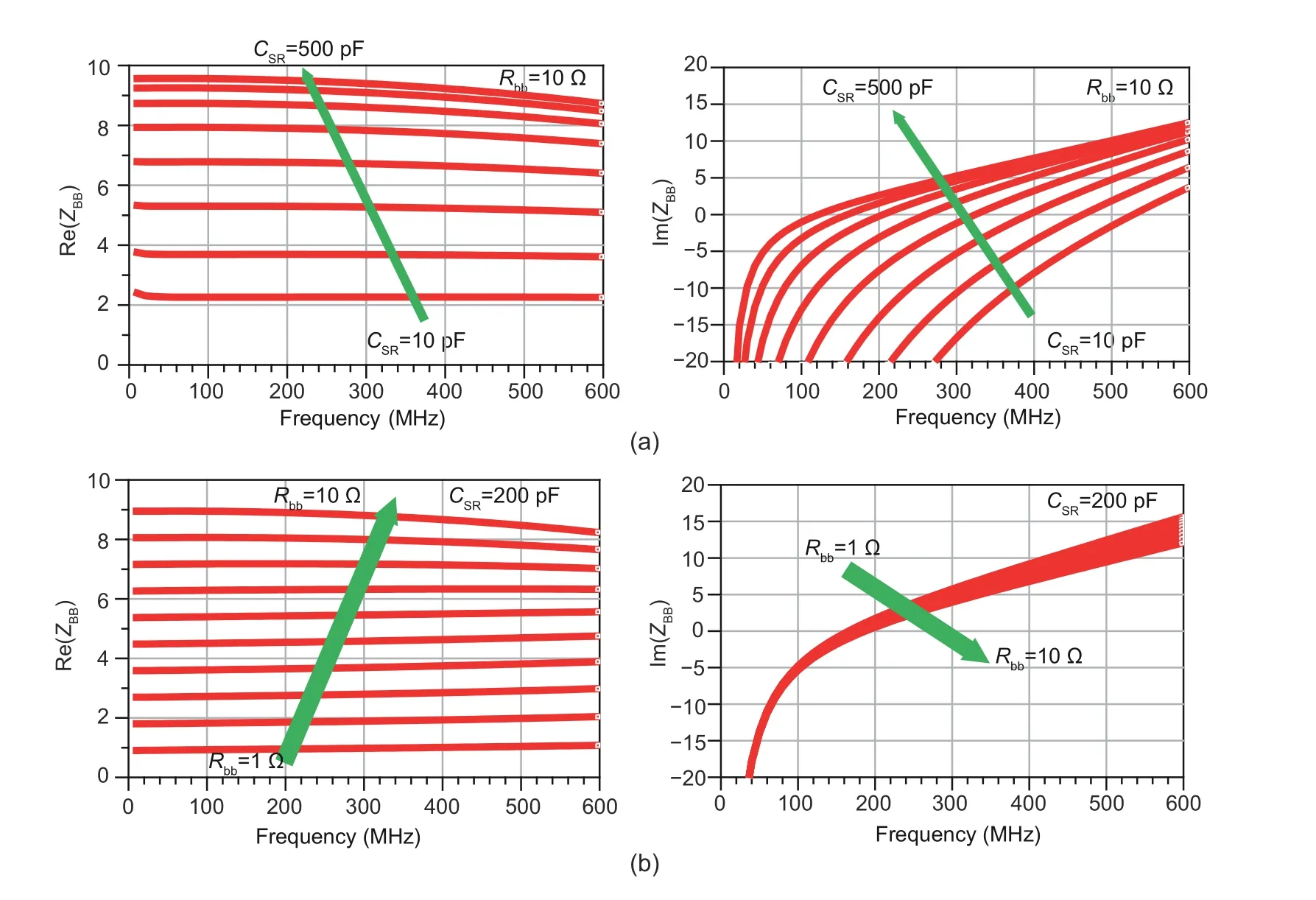
Fig.3 Impedance of a baseband impedance control unit: (a) ZBB vs. CSR;(b) ZBB vs. Rbb
The parameters of the BICUs can be determined using the following procedures: (1)First,choose the size of TL(length and width)according to the working frequency band,and select RF capacitorCRFaccording to the operating frequency band.(2) Determine the resonant frequency points of the BICUs and the number of BICUs,and calculateCSR.Let each resonant frequency point be dispersed in the target frequency band.(3)AdjustRbbto makeZBBas small as possible on the package plane and meet the target requirements,such as|ZBB,package|<5 Ω.
2.3 Design example
A PA working in the 1.8–2.3 GHz band is designed as an example to explain how to control baseband impedance.The output matching network is given in Fig.4 with four BICUs.Four BICUs are as close to the package of transistors as possible to achieve a small baseband impedance in the 0–500 MHz band.Accordingly,the impedance at the low-frequency band is provided in Fig.5a whenRbb=0.1 Ω andRbb=6 Ω.By comparing these two cases,it can be found that when the impedanceRbbis close to 0,the resonance phenomenon will appear in the circuit,leading to impedance spikes at some frequency points,i.e.,{55,130,235,380}MHz,which will worsen the PA performance in the concurrent mode.The fundamental and harmonic impedances are plotted in Fig.5b.It could be found that BICUs have little influence on harmonic impedance.
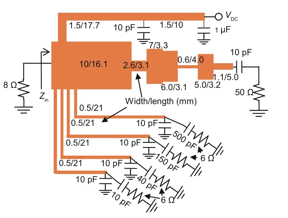
Fig.4 Output matching network with four baseband impedance control units
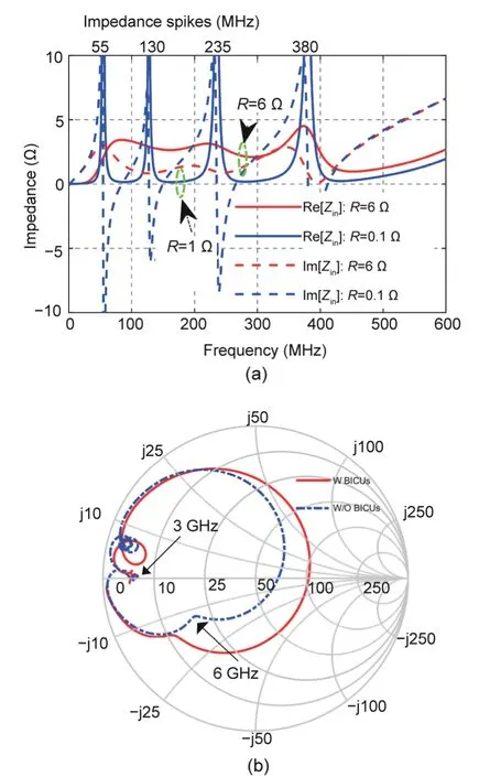
Fig.5 Output matching: (a) impedance with different Rbb;(b) S11 with/without baseband impedance control units in 1.5 to 7.0 GHz (w: with;w/o: without;BICUs: baseband impedance control units)
On the other hand,to evaluate the impact of the BICU on the fundamental impedance and loss of the matching network,the fundamental impedance andS21values are shown in Fig.6 (the circuit parameters are the same as those in Fig.4).The simulation results show that it has little effect on the fundamental impedance,while the maximum loss in the 1.5–2.6 GHz band is<0.05 dB.
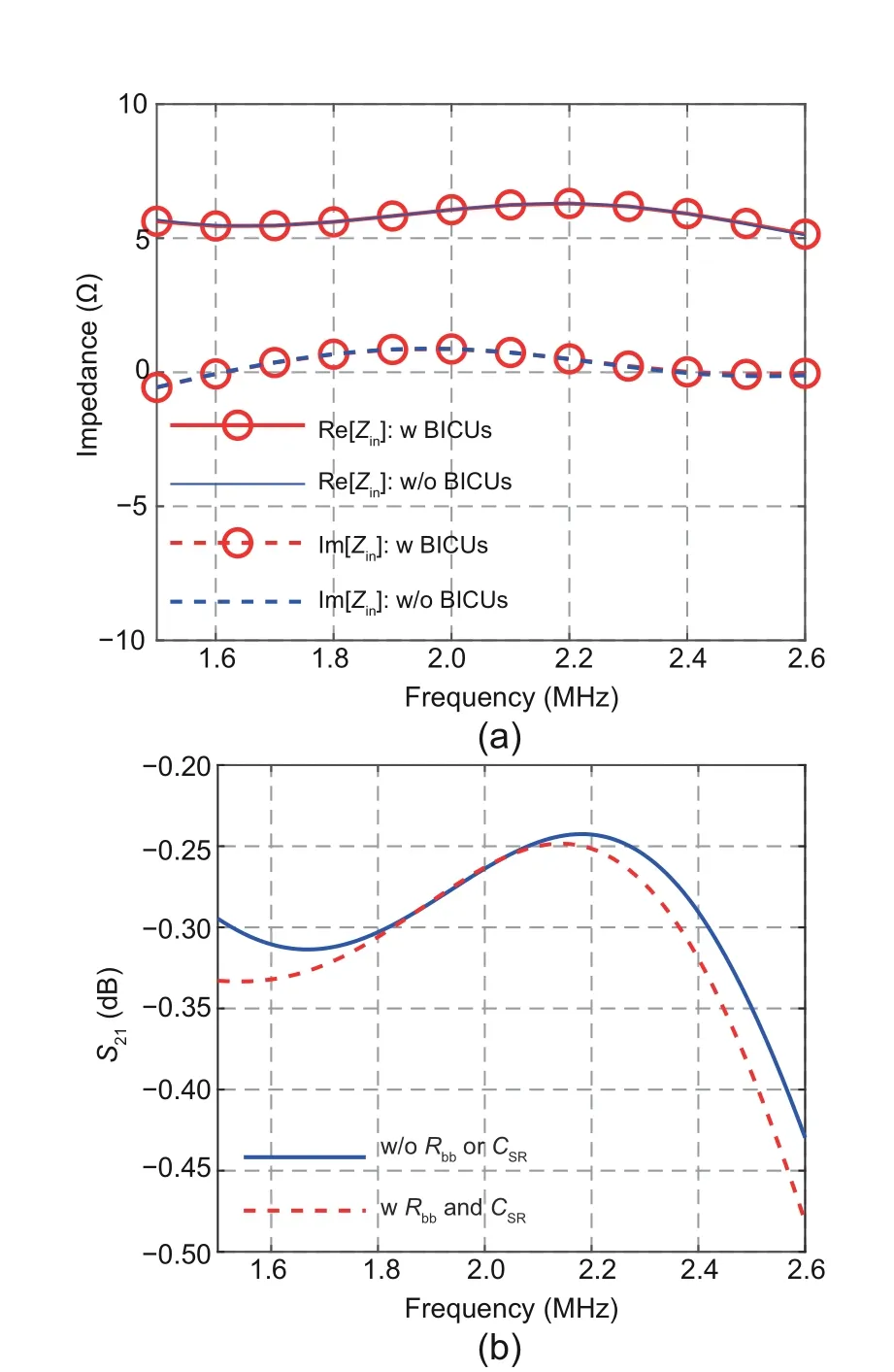
Fig.6 Output matching network simulation: (a)input impedance with/without CRF and Rbb;(b) S21 with/without CRF and Rbb (w: with;w/o: without;BICUs: baseband impedance control units)
This shows that by using this topology,the lowfrequency baseband impedance can be adjusted with little effect on fundamental frequency impedance.In other words,it can achieve good PA performance in the concurrent mode without affecting its performance in the narrowband mode.
Under two-tone excitation,the efficiency and IMD3 (the difference between the output power and three-order intermodulation product in dBc) with different numbers of BICUs are shown in Fig.7 when the output power of each tone is 35 or 38 dBm.Observing Figs.2b and 5a,we can see that the impedance within the 500 MHz frequency band is relatively small at three and four BICUs (their impedance is <5 Ω).From the simulation results,it can also be seen that their performance is similar.In actual experiments,to flexibly adjust the parameters of the circuit,we choose a topology structure of four BICUs.

Fig.7 Simulated efficiency(a)and IMD3(b)with different numbers of baseband impedance control units(BICUs) and output power
It is worth noting that when the number of BICUs exceeds 3,the parasitic reactance from the transistor packaging plane to the current source plane significantly impacts the baseband impedance.However,due to the commercial transistor limitations,the parasitic network part cannot be changed.This leads to inability to design baseband impedance.
3 Measurement results
The adopted printed circuit board (PCB) is Rogers 4350B with a thickness of 0.508 m (εr=3.66),and a Wolfspeed CGH40045 GaN transistor is used to verify our proposed approach.Fig.8 is a photograph of the implemented PA.BICUs are added in the input and output matching networks.

Fig.8 Fabricated printed circuit board
First,under the excitation of a single-tone continuous wave,the saturation output power and drain efficiency are presented in Fig.9.The measured saturated output power and efficiency range from 46.3 to 47.1 dBm and 68.2% to 71.6% within the 1.8–2.3 GHz band,respectively,where gain compression is about 3 dB.Because the efficiency curve of this band is relatively flat (about±1.7%),this band is selected to evaluate the performance of PA under two-tone excitation and increasing spacing.The simulated and measured results show that the PA efficiency is higher without BICUs than that with BICUs in continuous single-tone mode.
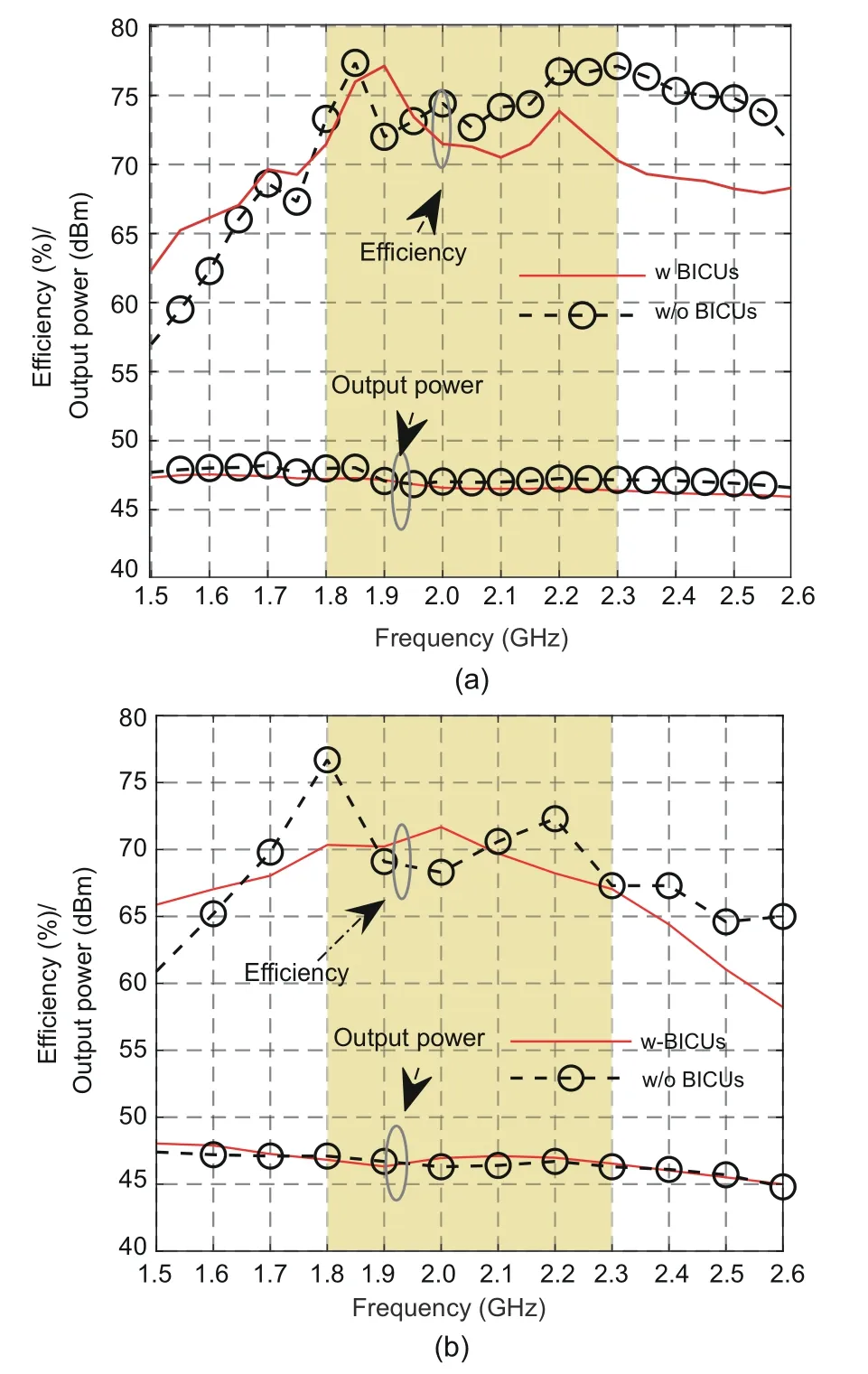
Fig.9 Efficiency and output power vs.frequency with/without baseband impedance control units (BICUs): (a) simulation;(b) measurement
Furthermore,with the excitation of a two-tone(F1andF2) continuous wave,the output powers of the two frequency bands are equal by independently adjusting the input signal power of the two frequency points.The test block diagram is given in Fig.10.With the increasing tone spacing from 10 to 500 MHz(i.e.,spacing=F2-F1),simulated and measured efficiency and IMD3 at two output power levels (35 and 38 dBm) are shown in Figs.11 and 12 respectively,where we determine whether to connect BICUs by cutting or not cutting the transmission lines in BICUs.It can be observed in Figs.11 and 12 that using BICUs can improve efficiency,at least,when the frequency is >180 MHz.The measured efficiency is about 28.5%when the output power per tone is 35 dBm (about 8.5 dB power back-off).The measured efficiency is about 40% when the output power per tone is 38 dBm(about 5.5 dB power backoff).When the output power of each tone is 35 and 38 dBm,IMD3 is about-34 and-27 dBc in the 10–300 MHz range and-22 and-22 dBc in the 300–500 MHz range,respectively.Compared with test and simulation results,efficiency values are compatible.The simulation results and test IMD3 are not consistent within the 300–500 MHz band.The main reasons are: (1)the parasitic parameters of the lumped elements used in the circuit have a significant influence in the 300–500 MHz band;(2) IMD3 is related to the impedance at the frequency ofF1+F2,which may have a large deviation from the simulation results.
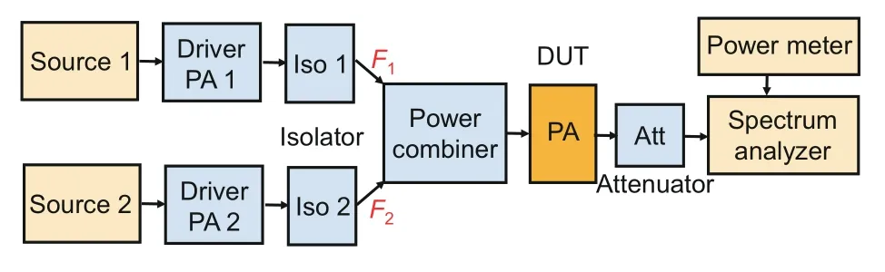
Fig.10 Test block diagram under two-tone excitation
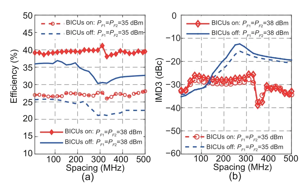
Fig.11 Simulated efficiency (a) and IMD3 (b) under concurrent two-tone excitation (F1=1.8 GHz, F2=F1+spacing)

Fig.12 Measured efficiency (a) and IMD3 (b) under concurrent two-tone excitation (F1=1.8 GHz, F2=F1+spacing)
Comparison is given in Table 1.It could be noted that the proposed topology is competent for wideband baseband impedance control.
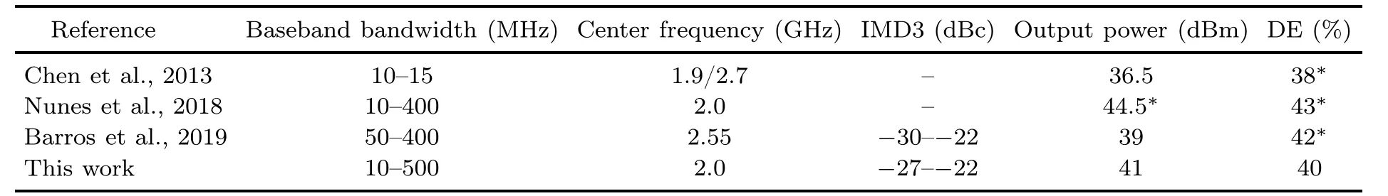
Table 1 Comparison with reported power amplifiers under two-tone excitation
4 Conclusions
In this paper,a novel baseband impedance control network topology is proposed,and a power amplifier design example is presented to explain the application of the topology.The experimental results show that the baseband impedance can be controlled up to 500 MHz with low impedance,and that there is no resonance generation when four parallel BICUs are used.In addition,the proposed topology can help avoid PA efficiency deterioration with an increase in the tone spacing.This topology offers an opportunity to control more complex baseband impedance with more BICUs,such as the application of tri-band concurrent mode.
Contributors
Yao YAO and Zhijiang DAI designed the research.Yao YAO drafted the paper.Mingyu LI helped organize the paper.Zhijiang DAI revised and finalized the paper.
Compliance with ethics guidelines
Yao YAO,Zhijiang DAI,and Mingyu LI declare that they have no conflict of interest.
Data availability
The data that support the findings of this study are available from the corresponding author upon reasonable request.
杂志排行

Frontiers of Information Technology & Electronic Engineering的其它文章
- Secure control and filtering for industrial metaverse
- The engineering of circular causality for specialization and design of complex systems:cad2CAS and casCAD2∗
- A low-noise,high-gain,and large-dynamic-range photodetector based on a JFET and a charge amplifier*
- Empowering smart city situational awareness via big mobile data∗
- Asynchronous gain-scheduled control of deepwater drilling riser system with hybrid event-triggered sampling and unreliable communication∗#
- Estimation of Hammerstein nonlinear systems with noises using filtering and recursive approaches for industrial control*