Silicon-based optoelectronic heterogeneous integration for optical interconnection
2024-02-29LeLiangLi李乐良GuiKeLi李贵柯ZhaoZhang张钊JianLiu刘剑NanJianWu吴南健KaiYouWang王开友NanQi祁楠andLiYuanLiu刘力源
Le-Liang Li(李乐良), Gui-Ke Li(李贵柯), Zhao Zhang(张钊), Jian Liu(刘剑),Nan-Jian Wu(吴南健), Kai-You Wang(王开友), Nan Qi(祁楠),†, and Li-Yuan Liu(刘力源)
1Institute of Semiconductors,Chinese Academy of Sciences,Beijing 100083,China
2Center of Material Science and Optoelectronics Engineering,University of Chinese Academy of Sciences,Beijing 100049,China
Keywords: silicon-based heterogeneous integration, heterogeneous integrated materials, heterogeneous integrated packaging,optical interconnection
1.Introduction
As the foundation stone of the information society, the development of integrated circuits has been following the Moore’s law, and has driven economic progress ubiquitously.However, since 2000, integrated circuits encounter process bottlenecks (frequency bottlenecks or power wall problems)and architectural bottlenecks (von Neumann memory wall problems).With the further development of advanced technology nodes from fin field effect transistor(FinFET)to gate all around field effect transistor (GAAFET), the miniaturization is stalling because of their physical limits,leakage,reliability,and yield problems.The global semiconductor industry has entered the post-Moore era.[1]
However, with the outbreak of data-intensive computing applications and communication in post-Moore era, such as artificial intelligence (AI), high performance computing(HPC), hyper-scale data centers, disaggregated memory and storage, it has led to the development of a variety of powerful, high-throughput, system-on-chip (SoC) solutions that redefine traditional computing architectures, such as GPU and machine learning(ML)ASIC scaling,disaggregation of computation and memory,etc.[2–5]In these new computing architectures, higher bandwidth density and energy efficiency are required, but traditional electrical interconnection will be extremely challenging because of the large signal losses in copper interconnects at high data rate, such as 112 Gb/s, make it hard to transmit data further than a few centimeters.[6]The next-generation high-performance interconnection requires a new form of universal interconnection that eliminates the bottlenecks created by electrical interconnection.[7]Optical interconnection takes the advantages of photons with high bandwidth,high speed,low power consumption,and low latency.It is widely used in optical communication and computing.[8–12]The optical interconnection is expected to continue the rapid development of information technology in the post-Moore era.
At present, optical interconnection mainly relies on the heterogeneous integration of discrete photonic integrated circuit (PIC) and electronic integrated circuit (EIC) by hybrid packaging.Discrete PIC, such as lasers, modulators, photodetectors,is mainly based on materials such as silicon,III/V compound,LiNbO3,and EIC is mainly based on CMOS process, SiGe process and III/V process.The advantage is that PIC and EIC can be optimized separately.However, as the requirements for area, power consumption, and bandwidth density further increase, this single material and integration method is hard to meet the demand.Silicon-based optoelectronic heterogeneous integration is the most promising way and has become a research hotspot in the world.[4,13]Heterogeneous integration includes two cases, one is that different material systems are physically bonded or grown to a common substrate and processed together to form the final component,[14,15]and the other is that it integrates components from different foundry technology platforms,usually post fabrication,using physical attach processes,i.e.,packaging.[16]
In this paper,we review the recent progress of the siliconbased optoelectronic heterogeneous integration for optical interconnection.The organization of this paper is as follows.In Section 1, we introduce the background and significance of the development of silicon-based optoelectronic heterogeneous integration chips.In Section 2,we present the advances of silicon-based heterogeneous integration with other materials, such as III–V active materials, LiNO3.In Section 3, we focus on the research progress of silicon based heterogeneous integrated packaging technology,such as 2.5D and 3D.In Section 4, we summarize and look forward to the silicon-based optoelectronic heterogeneous integration for optical interconnection.
2.Heterogeneous integrated materials enhance silicon photonic devices performance and add functionalities
Silicon photonics is compatible with CMOS technology,and it can employ the existing manufacturing infrastructure established by the CMOS electronics industry to achieve largescale mass production.It has the advantages of low cost,high manufacturing scale, high integration, high energy efficiency and high reliability.[17,18]Over the last decade, silicon-based optoelectronic devices have made many breakthroughs, such as detector and modulator.[19–24]However, the performance and functionalities of silicon-based optoelectronic integrated chips are limited by the silicon material itself, such as low loss high-speed modulator and integrated high density light source.But the rapid development of the information society has put forward higher requirements for photonic integrated devices in terms of speed,power consumption,footprint,and integration.It is difficult to meet these requirements by a single material system.Heterogeneous integration of silicon photonics with advanced CMOS, RF electronics and III–V optical sources and detectors has enabled complex systems,which is not possible with the native material.It can achieve high performance silicon photonics and then realize the true sense of silicon-based optoelectronic monolithic integration system.That is also a significant advantage of silicon photonics platforms compared to other platforms.Heterogeneous integration with co-packaged silicon photonics and electronics is the key towards future high performance optical interconnection.
Heterogeneous integration allows performance optimization for both passive and active devices.We will introduce the most recent results in high-performance silicon photonic devices using heterogeneous integration.
The typical silicon waveguide loss is on the order of 0.1 dB/cm to 1 dB/cm.[25]As the scale and complexity of integrated photonic circuits increase, the availability of low loss integrated photonic waveguides is critical.Silicon-based heterogeneous integrated silicon nitride waveguides have low loss, and they are compatible with CMOS processing.Recent advances in silicon nitride waveguides have demonstrated waveguide loss ranging from 0.1 dB/cm to 0.001 dB/cm(0.1 dB/m)by using CMOS processing.Silicon nitride waveguide with loss lower than 0.1 dB/cm has been reported.[26]A recent publication has reported losses as low as 0.1 dB/m using high-temperature treatment in CMOS foundries.[27]It is worth noting that ultra-low loss waveguides make some new technologies possible,such as on-chip soliton microcombs[28]and ultra-narrow linewidth integrated lasers,[29]which will be further discussed later.
Germanium has a higher mobility than silicon,so siliconbased heterogeneous integrated germanium devices, such as modulator and photodetector, have high bandwidth and high responsivity, and they are fully compatible with CMOS processing.A 56 Gbps high-speed Ge electro-absorption modulator(EAM)has been reported.[30]A recent publication has demonstrated a 110 Gbit/s NRZ and 160 Gbit/s PAM-4 SiGe electro-absorption modulator.[24]The bandwidth of the germanium photodetector (PD) has also been greatly improved,reaching 60 GHz[31]or even 265 GHz under the condition of low dark current and good responsivity.[32]Silicon-based heterogeneous integrated germanium effectively expands the operating wavelengths of silicon photonic EAM and PD, and it also greatly improves the bandwidth of the modulator and PD,thus meeting the needs of high-performance optical interconnection.In addition, silicon-based heterogeneous integration of other group IV materials,such as GeSn,also shows promising potential.
德公公招集义子及得力部下,分派护卫任务。德公公虽说一向阴险,但终究是个俗人,私心难除。鉴于老四死得不明不白,他让老五、老六、老八担任灯节禁区护卫头领,其他爪牙则在内城巡视。
Most of group III–V materials are direct bandgap,therefore heterogeneous integration III–V active materials onto silicon or silicon-on-insulator (SOI) provides optical gain and thus enables lasers and amplifiers, expanding the complexity and improving the performance of PICs,such as on-chip integrated high-performance InP directly modulated laser(DML),externally modulated laser (EML) and PD.Another advantage of heterogeneous III–V/Si lasers is the availability of on-chip Si mirrors or Si facets as the laser mirror.The degradation of cleaved facets in monolithic III–V lasers can thus be eliminated due to the excellent robustness of passive Si-based mirrors.In 2017, Ghent University demonstrated 56 Gb/s nonreturn to zero on–off keying (NRZ-OOK) either by direct modulation or by electro-absorption modulation based on a high bandwidth heterogeneously integrated III–V on silicon distributed feedback (DFB) laser.[33]Another type of Bragg grating-based laser is a distributed Bragg reflector(DBR)laser.DBR lasers have the potential to achieve narrow linewidth with ultra-long external cavity.Recently,University of California Santa Barbara (UCSB) has reported heterogeneous integrated III–V on silicon extended DBR lasers, with∼1 kHz linewidth and over 37 mW output power, as well as a ring-assisted DBR laser with less than 500 Hz linewidth.[34]The extended DBR lasers are fabricated by heterogeneously integrating III–V material on Si as a gain section plus a 15 mm long, low-kappa Bragg grating reflector in an ultralow-loss silicon waveguide.By incorporating thermally sensitive silicon waveguides in the laser cavity, heterogeneous integration allows for widely tunable lasers while maintaining low round-trip losses.A heterogeneous integrated coherent tunable laser(ICTL)has been demonstrated that provides a record 118 nm of wavelength tuning and Lorentzian linewidth below 95 Hz, with-155 dBc/Hz RIN, and a maximum chip power of∼12 mW.[35]As discussed in the previous, Si3N4waveguide loss can be lower than that of Si.Further noise reduction through laser active–passive integration can be achieved if Si3N4can be integrated within the laser cavity.Heterogeneous integrated IIIV/Si/Si3N4extended DBR lasers with high-QSiN resonators have been reported,[36]as shown in Fig.1.The extended DBR lasers have over 20 mW output powers with Lorentzian linewidth down to 400 Hz.
In addition to bonding,direct on-chip epitaxial heterogeneous integration quantum dot (QD) provides a new way, so it has become a research highlight.QD lasers offer new opportunities for improved performance towards lower threshold current density, narrower linewidth, higher temperature stability, better immunity to epitaxy and fabrication defects,and reduced linewidth enhancement factor.In 2016,Hewlett-Packard Lab demonstrated the first QD laser on a silicon substrate with efficient coupling of light to a silicon waveguide under the QD gain region, and continuous wave operation at 100◦C.[37]Subsequently, a series of silicon-based light sources were developed by University College London and the University of California using silicon-based direct epitaxial quantum dot technology.[38–40]It is worth noting that,a 1310 nm heterogeneous quantum-dot DFB laser on silicon with high efficiency and modulation capability has been reported,[41]25 Gb/s data-links isolator-free modulation with a metal-oxide semiconductor capacitor microring modulator has been achieved, as shown in Fig.2.A directly modulated QD/Si heterogeneous DFB laser with 3-dB modulation bandwidth of 13 GHz has also been demonstrated.[42]Fortunately,several foundries, such as Tower Semiconductor, AIM Photonics, CEA-LETI, IMEC and IME, are currently exploring the process of integrating III–V materials with CMOS.
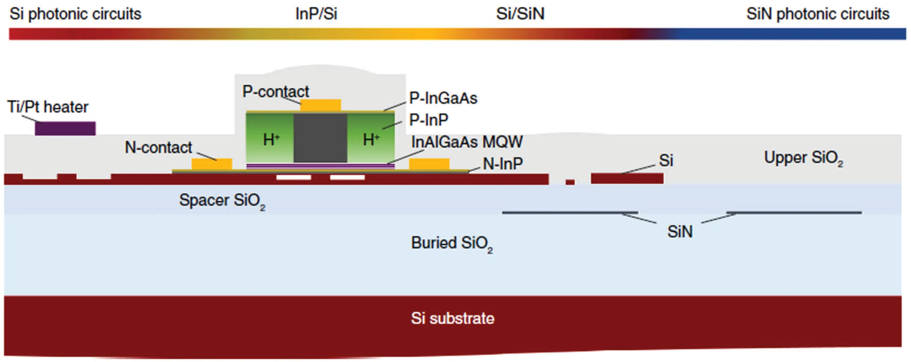
Fig.1.Heterogeneous integrated IIIV/Si/Si3N4 extended DBR lasers.[36]

Fig.3.On-chip comb laser for integrated transmitter.[14]
As previously discussed, low loss waveguide integrated gain materials make on-chip optical comb possible.Comb lasers are ideal for multi-wavelength data interconnects due to the natural fit with WDM systems.In 2017, an integrated III–V-on-silicon comb laser with a line spacing of only 1 GHz consisted of more than 1400 densely and evenly spaced optical lines with below 400-kHz optical linewidth has been demonstrated.[43]In 2018, UCSB designed a lowloss low-reflection taper to seamlessly integrate the ultra-lowloss waveguide with standard heterogeneous Si/III–V integrated photonics platform.[44]They also realized low threshold power optical frequency combs on silicon-based heterogeneously integrated AlGaAs-on-insulator platform.[45]Recently, due to the advantages of quantum dot as mentioned above, QD-based III-V/Si comb lasers have demonstrated remarkably flat optical spectra,and the optical output is continuous wave(CW).[46]On-chip modulators have been added to realize a fully integrated transmitter and open eye diagrams at 10 Gb/s for the 15 highest power channels, and 14 of those channels have a BER 10-12or better, as shown in Fig.3.It is worth noting that,a recent publication has reported the application of comb laser to silicon photonic systems,[47]which fully demonstrates the broad prospects of silicon based heterogenous integration of group III–V materials.
Lithium niobate (LiNbO3) has excellent electro-optical properties.Silicon-based heterogeneous integrated thin film lithium niobate(TF-LiNbO3)has become a research hotspot.TF-LiNbO3greatly improves the performance of silicon-based modulator, with ultrahigh bandwidth, low loss, and high linearity, and has made great progress in recent years.In 2018, Harvard University demonstrated monolithically integrated TF-LiNbO3electro-optic modulators that feature a CMOS-compatible drive voltage, support data rates up to 210 Gb/s PAM-8, as shown in Fig.4.[48]In 2020, University of Rochester reported an ultra-miniature silicon-based TFLiNbO3modulator based on photonic crystals, with a tiny electro-optic modal volume of only 0.58 µm3.[49]The Sun Yat-sen University demonstrated integrated TF-LiNbO3inphase/quadrature modulators.The bandwidth of silicon-based coherent TF-LiNbO3modulator exceeds the equipment test range 67 GHz for 7.5 mm length, and it supports modulation data rate up to 320 Gbps.[50]Coherent communication has higher data rate.A dual-polarization TF-LiNbO3coherent modulator has been reported,with sub-1-V driving voltage and 110-GHz bandwidth, enabling a single-wavelength 1.96-Tb/s net data rate with ultrahigh energy efficiency.[51]Recently, a TF-LiNbO3Mach–Zehnder modulator with a 3 dB bandwidth exceeding 110 GHz has been demonstrated,which shows the potential of boosting the throughput and reducing cost.[52]Due to the outstanding advantages of TF-LiNbO3, it will become the preferred solution for high-performance on-chip modulators.

Fig.4.CMOS compatible TF-LiNbO3 modulator.[48]
3.Heterogeneous integrated packaging improves the performance of optical interconnection
In additional to heterogeneous integrated materials, heterogeneous integrated packaging also shows advantages in optical interconnection.In early telecom and datacom applications, optical interconnection was realized by discrete electronic integrated chips (EICs) and photonics integrated chips(PICs)connection,which limited performance in terms of energy efficiency, bandwidth, and latency.To improve performance of optical interconnection, efforts have been made to bring electrical–optical chiplets closer by heterogeneous integration between EICs and PICs.We will introduce it from 2D/2.5D/3D integration to monolithic integration.
3.1.The 2D integration
This approach involves the EIC and PIC being connected on a printed circuit board (PCB) through a wire-bonding assembly process.The advantage of 2D integration is that it can design and prepare EIC and PIC separately, which has high flexibility, and the 2D integrated packaging process is relatively simple.Importantly, compared with discrete devices,2D integration greatly reduces the distance between EICs and PICs,so it has a great improvement in performance,and it has been widely used in academic research and commercial applications as discussed below.
In 2013, University of Pennsylvania and Cisco demonstrated a 20 Gb/s data rate and sub-pJ/bit modulation energy optical transmitter through 2D integrated CMOS drivers and CMOS compatible multi-segment silicon photonic modulator.[53]Note that, CMOS driver and silicon photonic modulator were fabricated by different processes.In 2015,the University of Southampton reported a 2D integrated optical transmitter achieving 30 Gb/s with the power consumption of main driver being 323 mW.[54]In 2016, a low-cost, smallsize 10×11.3 Gbps dense wavelength division multiplexing(DWDM)optical transmitter through 2D integrated SiGe BiCMOS driver with MZ modulator has been demonstrated.[55]It showed the integration density advantage of heterogeneous integration.In 2019, Intel presented a 112 Gb/s PAM4 optical receiver by using a 35 GHz Ge-on-Si-PD wire-bonded to a 28 nm CMOS linear TIA, and the energy efficiency is 0.96 pJ/bit.[56]It demonstrated the bandwidth and the energy efficiency advantages of heterogeneous integration.In 2020,Intel demonstrated a 112 Gb/s PAM4 compact low power optical transmitter using silicon photonic MRM with on-chip laser and 28 nm CMOS driver.[57]Importantly,it demonstrated the very high performance of heterogeneous integrated materials and packaging, such as small footprint, low power, and high bandwidth.In addition, removing a fiber-to-chip optical coupler between the on-chip laser and modulator leads to less overall loss, which can improve the link budget.The emitted light from a semiconductor laser is also highly polarized, eliminating any polarization-based ambiguity at the input to the modulator.Note that, Intel released large-scale,high-volume heterogeneous 100 G and 400 G silicon photonic quad small form-factor pluggable (QSFP) transceivers with heterogeneously integrated laser in CMOS foundry in 2016 and 2020, respectively, which are shipping millions of units per year.[58]
Over the past few years,great progress has been made on 2D integration for optical interconnection in China.
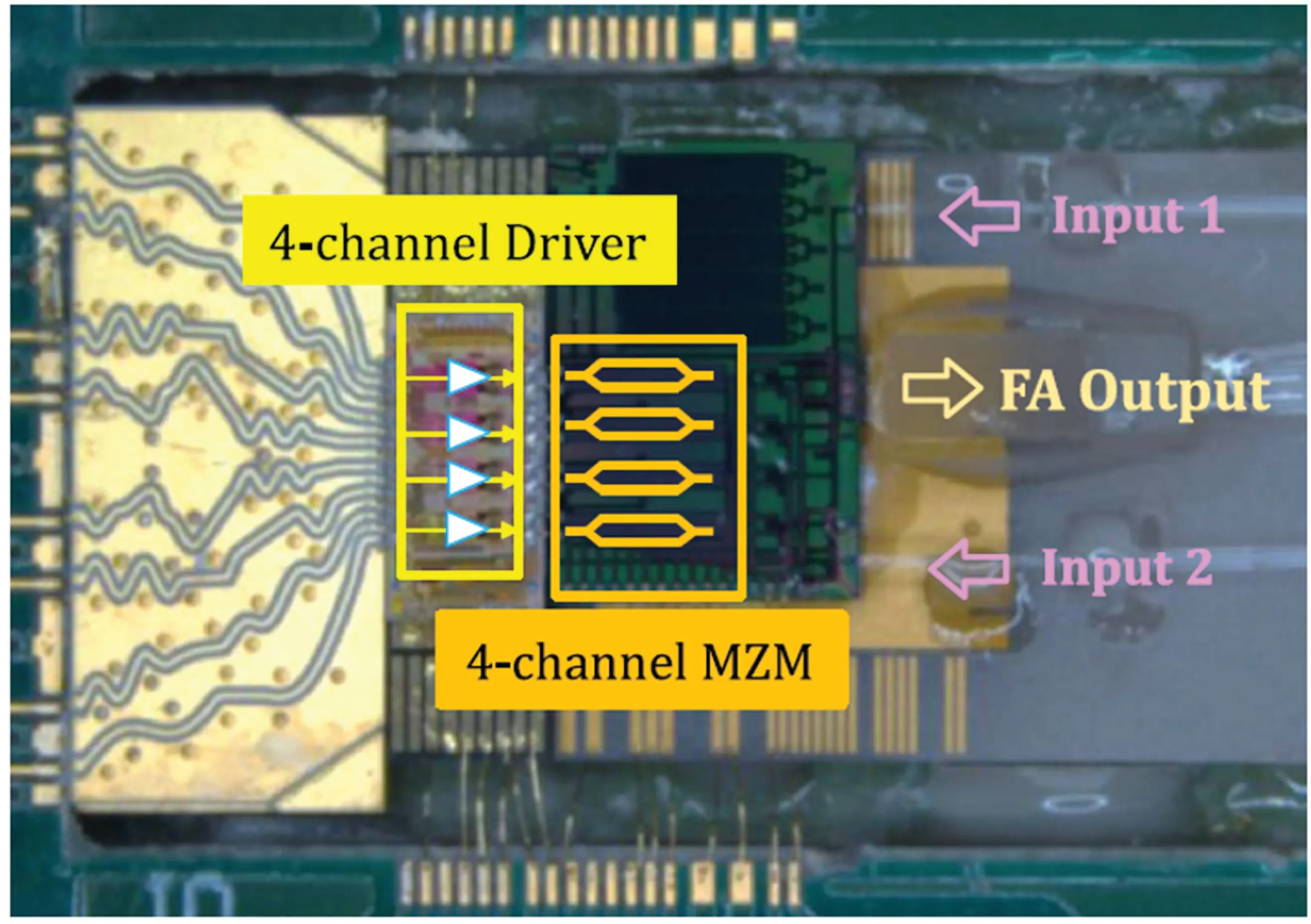
Fig.5.A 800G silicon photonic transmitter.[61]
In 2021,Huazhong University of Science and Technology demonstrated a co-designed optical receiver,which is hybridintegrated with a silicon-photonic PD and silicon-germanium trans-impedance amplifier(TIA),and 100 Gb/s NRZ operation is successfully achieved with a soft-decision forward error correction(SD-FEC)threshold,as shown in Fig.6.[62]The Southeast University presented a low noise 28 Gbaud/s linear receiver front-end for PAM4 signal.The PAM4 optical receiver front-end achieves a maximum differential transimpedance gain of 76 dBΩ and-3 dB bandwidth of 27 GHz.[63]Southern University of Science and Technology demonstrated an CMOS process optical receiver analog front-end.[64]Wuhan University designed a 25 Gb/s inductorless optical receiver,with a high sensitivity and wide dynamic range.[65]
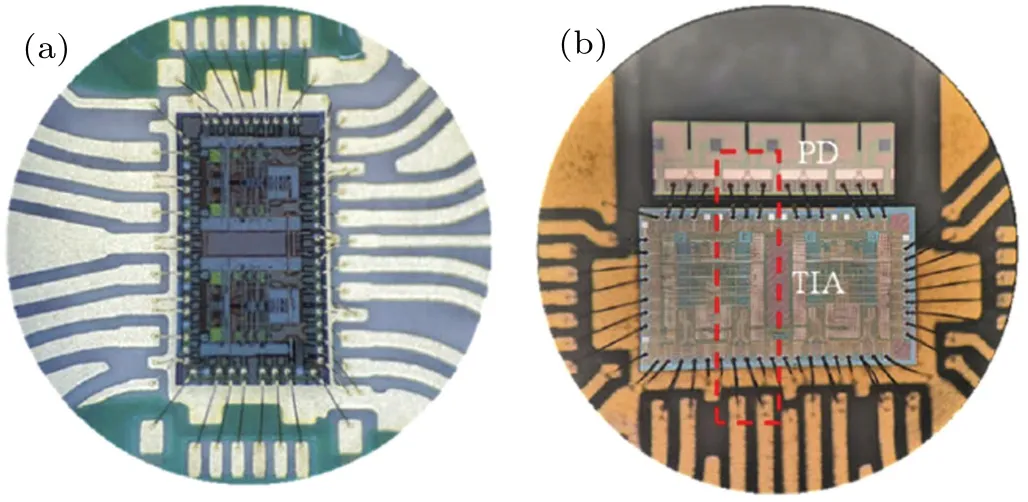
Fig.6.A 100 Gb/s co-designed optical receiver.[62]
In 2022, Institute of Semiconductors, Chinese Academy of Sciences proposed a high bandwidth lumped 50 Gbps PAM-4 optical transmitter.[66]By grouping these lumped-segment Mach–Zehnder modulator (LS-MZM) segments in the thermometer code,high linearity modulation is achieved.A reconfigurable silicon photonics transmitter for short-reach optical interconnects was also presented.[67]The driver employs a reconfigurable distributed topology to achieve high swing,wide bandwidth, and flexible operation.A hybrid-integrated optical transceiver front-end for beyond-400G short-reach optical links with 8-channel laser drivers and the transimpedance amplifier (TIA) was also demonstrated.[68]Xi’an Jiaotong University designed a low-power TIA chip for 50G PON.[69]
In 2023, Peking University demonstrated a 16-channel silicon transmitter based on co-designed PICs and electrical chiplets.The power consumption of the Si transmitter with a high integration density featuring a throughput up to 800 Gb/s is only 5.35 pJ/bit.[70]
The 2D integration packaging is promising and cost,so it will exist for a long time.Therefore, how to further improve the performance is an important research direction in the future.
3.2.The 2.5D integration
Although 2D integration packaging is economic, but the link between EICs and PICs is longer,which incites parasitic inductances and capacitances.And it also limits the shoreline density of edge electrical interconnections where the EICs and PICs can be interconnected, restricting its scalability.Therefore, advanced packaging forms have been proposed.2.5D packaging involves the integration of EICs and PICs on an interposer, which mediates electrical signals between the EIC and PIC as well as PCB.At present,2.5D integrated approach is an important method to develop packaging solutions for current state-of-the-art photonic system.This is due to the scalability and flexibility of the assembly of photonic and electronic interconnects associated with this approach.The electrical losses can be reduced by using a suitable low-loss material such as high resistivity silicon,low-temperature co-fired ceramic(LTCC)or glass as an interposer.
In 2017, the Singapore Institute of Microelectronics implemented a 2.5D silicon optical interposer for 400 Gbps,achieving 50 Gbps per channel.[71]In 2022, Broadcom introduced a 2.5D integrated 25.6 Tbps optical switch for data center.[72]In 2023,University of Toronto demonstrated a linear TIA receiver based on CMOS technology, which realizes the rate of 112 bps and the sensitivity is as low as-8.2 dBm.[73]In 2023, Marvell presented their work in the area of heterogeneous optical integration, where higher levels of integration also allow for closer placement of devices which minimizes the parasitic power consumed and realizes higher speed,as shown in Fig.7.[16]
Although the performance of 2.5D package has no obvious advantages, mainly because the demand is not so strong,and the technology has yet to be further mature.Therefore,how to further improve the performance of 2.5D packaging will become an important research direction in the future, including interposer and integration methods.This is particularly important in China because there are few reports on advanced packaging in China.
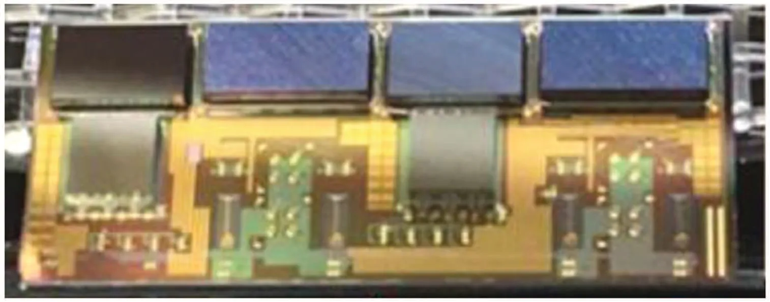
Fig.7.The 2.5D assembly of the optical engine.[16]
3.3.The 3D integration
This approach involves the EIC stacked on top of the PIC through copper pillar bumps allowing the electrical signals to be transmitted through redistribution lines and through silicon vias(TSVs)in the EIC.So that will considerably shorten the traces.It is worth noting that, 3D integration can greatly improve the bandwidth density.
In 2018, Fujitsu developed a high-density optical transceiver of 363 Gbps/cm2by 3D integration, and all 16 channels error-free operations with low crosstalk penalties were demonstrated simultaneously, as shown in Fig.8.[74]In 2021, Columbia University presented a compact, 3Dintegrated CMOS silicon photonic transceiver for DWDM interconnects.The transceiver interleaves 64 parallel wavelength channels enabling the energy efficient scaling of multi-Tbps/mm2bandwidth density for future co-packaged chipsets.[75]In the same year, Cisco proposed a new solution to reduce the interconnect loss in both transmitter and receiver paths and a new low-power driver architecture to realize 800G optical links.[76]In 2021,Intel demonstrated a silicon photonic engine for high bandwidth density 800 Gbps using 3D integration.[13]Obviously, 3D packaging greatly improves bandwidth density and reduces power consumption,and higher performance is expected to be achieved through research on 3D packaging materials and integration methods.
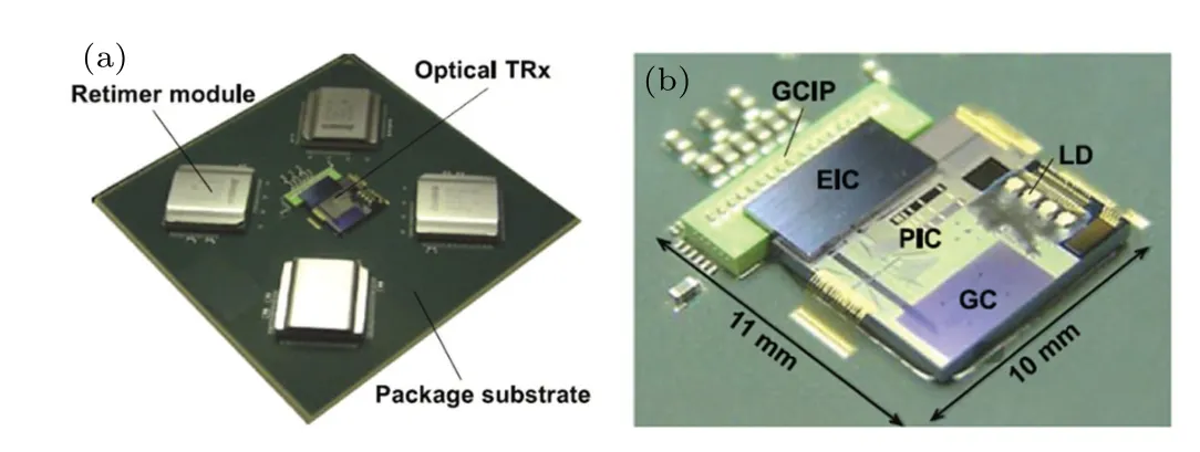
Fig.8.Photographs of(a)perspective view,and(b)magnified view of a developed optical TRx.[74]
3.4.Monolithic integration
This approach involves fabricating the electronic and photonic elements together on the same platform, using state-ofthe-art processing techniques.The electrical losses and parasitics are the lowest in this case due to the co-location of both functionalities on the same chip.So it will have a better performance in terms of energy efficiency and bandwidth density.At the same time,the design of EICs and PICs will lose some flexibility due to the varied node sizes.
In 2013, MIT demonstrated a monolithically integrated 2.5 Gb/s optical modulator with an all-digital driver circuit,operating with an energy-cost of 1.23 pJ/bit and better than 3 dB extinction ratio in a commercial 45 nm SOI process.[77]In 2016, IBM demonstrated a monolithic CMOS-integrated transmitter to achieve single-channel 32 Gb/s error-free transmission with insertion loss as low as 3.8 dB.[78]In 2016,University of California Berkeley proposed a monolithically integrated auto-tuning micro-ring DWDM transmitter with subpJ/bit energy efficiency and a high-density, high-sensitivity full-differential splitter receiver based on CMOS 45 nm SOI process.[79,80]It is worth noting that, the receiver improves the sensitivity by fully differential suppression of commonmode and power noise.This is an advantage of monolithic integration.In 2016, IHP demonstrated a silicon photonic transmitter with monolithically integrated segmented linear driver and Mach–Zehnder modulator (MZM), achieving 30 pJ/bit energy efficiency at 50 Gb/s.[81]In 2018, University Paderborn demonstrated the first monolithically integrated coherent receiver with bitrates up to 128 Gb/s for a single polarization.[82]In 2018, University of California Berkeley demonstrated an optical NRZ transmitter based on micro-ring modulator in a monolithic process, achieving 330 fJ/bit energy efficiency and 6.7 Tbps/mm2bandwidth density.[83]In 2020, Ayar Labs demonstrated a monolithically integrated low power,Tbit-level optical interconnection.[84]In 2023,Ranovus demonstrated a monolithically integrated 800G optical interconnection with high bandwidth density and good energy efficiency.[2]
Due to the limitation of the process, the research on monolithic integration in China started late.Institute of Semiconductors, Chinese Academy of Sciences began to explore monolithic integration in 2018.In 2019, the optical receiver integrated silicon photodetector (PD) and trans-impedance amplifier(TIA)into a single chip has been designed to achieve high bandwidth density and good energy efficiency.The test results showed that the data rate of the receiver can reach 64 Gb/s PAM4 per channel and the energy consumption is lower than 100 mW.By optimizing the circuit, it should be able to achieve 112 Gb/s or even 224 Gb/s per channel in the future.
Monolithic integration has excellent performance.The development of monolithic integration process,including heterogenous integration of other materials,will have a broad development space.
4.Conclusion and perspectives
In the post-Moore era, with the rapid growth of highperformance interconnection demand,optical interconnection has ushered in the best opportunity for development.To date,heterogeneous integration of materials such as silicon nitride,germanium,III–V compounds,and lithium niobate,as well as heterogeneous integrated packaging technologies such as 2D,2.5D,3D,and monolithic integrations,have achieved high performance, high bandwidth density, and low power consumption.These advances have had a revolutionary impact on the current integrated circuit technology.However,heterogeneous integration still faces many challenges.First,in terms of material epitaxy.Increasing waveguide thickness is an effective method for further reducing the loss of silicon nitride waveguides,but silicon nitride waveguides face serious stress problems,and they will crack when the films are thick.It is still difficult to grow thick silicon nitride at low temperature.Directbandgap IV group alloys such as GeSn epitaxy still have a large number of dislocations.The problems of lattice mismatch, thermal mismatch and reverse phase domain exist in the heterogeneous epitaxy of III–V materials,and it is difficult by bonding, making low product yield.Currently, thin-film lithium niobate is prepared by bonding, which is also hard to improve production yield, resulting in high cost.In addition,the device manufacturing process of thin-film lithium niobate is not yet mature, and a standard process has not been established, making large-scale production difficult.Secondly, in terms of packaging integration.Advanced packaging(such as chiplet)still faces a series of problems such as heat dissipation,pressure,and reliability,and the standards have not been established.The advanced materials and devices required for advanced optoelectronic packaging are still in the development stage,and the industrial chain is not mature.These hinder the large-scale deployment of advanced packaging.
In the future, heterogeneous integration has a package of issues to be studied and broken through to achieve more functions, better performance, higher energy efficiency and lower costs.First of all, in terms of material growth integration.It is also necessary to explore the growth mechanism,growth method or bonding way to improve material quality and reduce the complexity of the manufacturing process.Researching high heat dissipation capacity, high performance,and high reliability packaging materials is the key to the future application of heterogeneous integration.Furthermore,facing new applications, new types of devices need to be developed, including but not limited to low-loss, micro-scale,multi-functional, and multi-dimensional reconfigurable photonic devices such as low-loss waveguides, couplers, microring(disk)modulators,and developing low-cost,miniaturized,simple and reliable packaging connectors.Breakthroughs in traditional device integration methods, new integration architectures are studied,such as multi-bus optical paths to reduce insertion loss and improve parallelism,and multi-FSR designs to reduce crosstalk,etc.Finally,in terms of system integration,multi-material system integration (lasers and amplifiers), and ultra-large-scale integration(12 inches)will become the development trend,so the following three aspects need to focus on research.(1) Ultra-high-density (Tbps/mm2) and low-energy consumption(pJ/bit)on-chip optical interconnect technology,to achieve an order of magnitude increase in bus bandwidth density and promote revolutionary innovation in the architecture of computing systems.(2) High-bandwidth (Pb/s) and low-latency(10 ns)key processes and technologies for optical interconnects between chips,enhancing the computing power of AI chips.(3) The 12-inch CMOS compatible electronicphotonic convergence integration, realizing disruptive architecture innovation of chips.However, multi-material integration and advanced packaging will be the key enablers for success.
Acknowledgements
Project supported in part by the National Key Research and Development Program of China (Grant No.2021YFB2206504), the National Natural Science Foundation of China (Grant No.62235017), and the China Postdoctoral Science Foundation(Grant No.2021M703125).
猜你喜欢
杂志排行
Chinese Physics B的其它文章
- Unconventional photon blockade in the two-photon Jaynes–Cummings model with two-frequency cavity drivings and atom driving
- Effective dynamics for a spin-1/2 particle constrained to a curved layer with inhomogeneous thickness
- Genuine entanglement under squeezed generalized amplitude damping channels with memory
- Quantum algorithm for minimum dominating set problem with circuit design
- Protected simultaneous quantum remote state preparation scheme by weak and reversal measurements in noisy environments
- Gray code based gradient-free optimization algorithm for parameterized quantum circuit