Correspondence:A low-profile dual-polarization programmable dual-beam scanning antenna array*#
2023-11-06ShichaoZHUYuanfanNINGHongboCHUPeiXIAOGaoshengLI
Shichao ZHU,Yuanfan NING,Hongbo CHU,Pei XIAO,Gaosheng LI
College of Electrical and Information Engineering,Hunan University,Changsha 410082,China
A low-profile dual-polarization dual-beam scanning antenna array based on holographic control theory is presented in this paper.The radiating elements are ingeniously designed to achieve reconfigurable polarization and modulation of the radiation phase by controlling the state of the PIN diodes integrated on each element.A 72-channel series-parallel equal-amplitude and in-phase feeding network is integrated with the radiating array to achieve low-profile characteristics.The two-dimensional (2D) dynamic and accurate deflection of the beam is achieved by a designed direct current (DC) bias circuit that digitally encodes the antenna array using the single-chip microcontroller.A 2-element subarray and a 6×12 array have been fabricated and the digitally controllable radiation pattern of this antenna system has been experimentally verified.The antenna system can achieve the beam scanning of -30° to 30°with a step-scan of 5° at 11 GHz.The proposed antenna system is characterized by low profile,low cost,easy integration,and accurate beam steering,and holds broad application prospects in radar systems,smart antennas,and other fields.
1 Introduction
A beam scanning antenna can adjust the direction of radiation over a physical aperture according to practical requirements and serve an important role in communication fields such as radar (Han et al.,2019;Wu et al.,2020;Xu P et al.,2020).The traditional method is to achieve beam scanning by mechanical scanning or phase shifters,such as a phased array(Latha et al.,2021),which is the most mature beam scanning antenna available,but it suffers from disadvantages such as complex design and high cost (Hum and Perruisseau-Carrier,2014;Rocca et al.,2016;Yang HN et al.,2020;Mirmozafari et al.,2021).In recent years,with the rapid development of wireless communication technology,the demand for high-gain,widecoverage,and high-capacity antennas is increasing,and a lot of reflectarray,transmitarray,and microstriparray antennas based on metasurface elements (discrete phase characteristic) have been designed to achieve good beam reconfiguration and scanning effect (Wan et al.,2016,2021;Yang X et al.,2018;Liu et al.,2020a).Compared with a phased array,the cost and complexity of such beam scanning antennas are greatly reduced (Li et al.,2021).Discrete phase states are achieved by tunable components integrated into the antenna,such as liquid crystal materials (Bildik et al.,2015;Gao et al.,2018),PIN diodes (Bai et al.,2020;Wang ZL et al.,2020;Wang ZY et al.,2020),and varactors (Dai et al.,2018;Zhao et al.,2019).
In Yang HH et al.(2017),a 1-bit dual-frequency electronically reconfigurable reflectarray antenna was proposed.The elements in the array have two states and the reflection phase difference between the two states is 180°.State switching is achieved by controlling an integrated PIN diode.The reflectarray antenna has 1600 elements,and the real-time dynamic adjustment of the beam is realized through the field programmable gate array (FPGA).In addition to reflectarray,there are many tunable transmitarray antennas(Iqbal et al.,2018;Nguyen and Pichot,2019;Liu et al.,2020b).A 2D beam-steering Fresnel-zone-plate antenna requiring only 180° phase tunability was proposed in Ma et al.(2021),and this array can achieve 45° deflection in both planes.However,both reflectarray and transmitarray antennas need an additional primary feed,which makes the overall profile of the antenna higher and requires installation considerations,and thus greatly limits the application of the antenna.
Consequently,low-profile pattern reconfigurable microstrip array antennas that do not require a primary feed have received attention (Hu et al.,2018;Geng et al.,2019;Lin et al.,2020;Niu et al.,2021).In Zhang et al.(2020),a reconfigurable planar array antenna with a low profile and high gain pattern was introduced.The radiating elements include digital “0” and “1”elements,which are realized by integrating PIN diodes on the microstrip line to control the radio frequency(RF) signal flow path.Real-time switching of different radiation beams can be achieved by dynamically encoding these digital elements.In Pan et al.(2022),a one-dimensional (1D) single-polarization beam scanning array for the Internet of Things was proposed.The two states of the antenna element belong to the opposite phase radiation sources and the beam scanning is realized by the coding method of holographic antenna theory.However,the antenna needs to be connected to the power divider through the RF cable,which adds complexity and is not conducive to system integration.
Based on the above research,a dual-polarization 1-bit element is proposed in this work.Four PIN diodes are integrated on the element.By adjusting the ON/OFF state of the diode in the same polarization direction,it is possible to change the different radiation states(opposite phase) and obtain 1-bit phase encoding characteristics.Because the element has adjustable diodes in both polarization directions,a dual-polarization function with horizontal/vertical polarization (HP/VP) is possible to achieve.Based on holographic modulation theory,the elements are coded,and the encoding is dynamically adjusted in real time using a microcontroller to realize dynamic beam scanning.The microstrip array,corresponding series-parallel feeding network,and DC bias circuit are designed,fabricated,and measured at X-band (11 GHz).The array is capable of achieving excellent dual-polarization beam scanning characteristics in both planes.In general,this antenna offers the advantages of a low profile,dual polarization,and easy integration.
2 Design of the dual-polarization element
2.1 Structure of the element
Fig.1a shows the overall view of the proposed radiation element.The element consists of substrate 1,substrate 2,bonding film,and four layers of the metal.Both substrates 1 and 2 are Rogers 4350B.The two substrates are bonded by Rogers 4450F bonding film.Fig.1b shows the radiation patch structure printed on the upper layer of substrate 1.The RF signal is fed to the antenna element through the microstrip line printed on the bottom layer of substrate 2 and the feed probe at the center,as shown in Fig.1c.The feed probe is also used as part of the DC bias circuit,and the other end of the microstrip line is connected to the ground through a high impedance line.The open-circuit line of the radial stub added to the high-impedance line corresponds to an open circuit at the bias point,so that the leakage of the RF signal is prevented.

Fig.1 Dual-polarization reconfigurable element: (a) overall configuration;(b) configuration of the radiation structure;(c) configuration of the feed structure;(d) configuration of the DC bias layer;(e) side view of the element;(f) equivalent circuit of the PIN diode;(g) layout and control schematic of PIN diodes
To achieve impedance matching,the microstrip line structure adopts a stepped impedance transition.Four PIN diodes are integrated on the radiation patch,two in each of the HP and VP directions,and the radiation phase difference characteristic of π is achieved by controlling the ON/OFF function of the PIN diodes.To achieve independent control of the four PIN diodes,the outer ring of the radiation patch is divided into two parts,and the two parts are connected by two capacitors,which ensures that the RF circuit is not affected,and increases the freedom of the DC bias circuit design.To achieve consistency of the dual-polarization performance of the antenna element,it is essential that the element should have a symmetrical structure as much as possible.Therefore,four high-impedance bias lines are designed and connected to the DC bias circuit printed on the upper layer of substrate 2 using metallized vias.Bias lines 1 and 2,and 3 and 4,are connected separately,finally forming two DC bias ports P1 and P2 on the DC bias layer,as shown in Fig.1d.The radial stub on the high-impedance lines is added to improve isolation between the RF and DC signals.The DC voltage reaches the radiation patch through the DC bias layer and metallized vias to control the PIN diodes,and then passes through the feed probe to the ground to form a complete DC path.The equivalent parameters of the PIN diodes are shown in Fig.1f.The forward bias state of the PIN diodes can be equivalent to the series of 5.2-Ω resistance and 30-pH inductance,and it is equivalent to the series of 30-pH inductance and 40-fF capacitance when reversely biased.
2.2 Simulation analysis of the element
During normal operation,the element needs only to turn on a PIN diode.Fig.1g shows the layout and control schematic of the PIN diode,in which the HP state of the element is determined by PIN 1 and PIN 3,and the VP state by PIN 2 and PIN 4.Because the radiation characteristics of the element are essentially the same when operating in the HP and VP states,only the element operating in the HP state is described here to make things easier.It is defined that PIN 1 is turned on and the others are turned off as state 0;otherwise,PIN 3 is turned on and others are turned off as state 1.Table 1 shows the PIN diode states under different DC bias voltages.With three DC bias voltages, the state switching of the element in HP/VP can be satisfied.
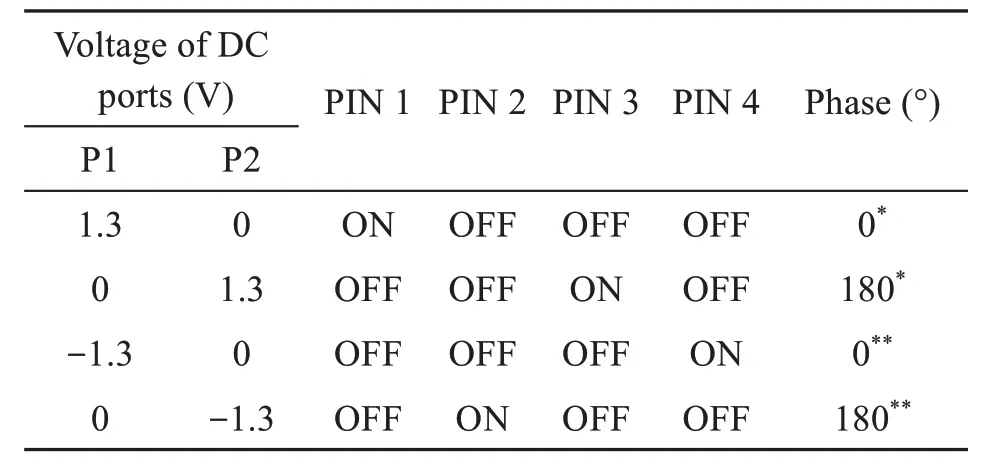
Table 1 DC port voltages corresponding to PIN diode states
Different resonant frequencies can be achieved by adjusting the size of the antenna element,and a detailed description of the effect of element sizerwon the operating frequency band can be found in Section 1 of the supplementary materials.
In the simulation,port 1 is the RF signal port of the array,and ports 2 and 3 are DC bias ports of the array.As seen in Fig.2a,theS11’s of the antenna element in the HP and VP are basically the same,and the -10-dB impedance bandwidth is 10.89-11.15 GHz.Meanwhile,in the operating band,S21is less than-30 dB,which means that the DC bias of the element has a good effect.The radiation patterns of the four states do not differ much,and the maximum gain reaches 4.7 dBi.For the dual-polarization characteristics,the cross-polarization performance is good in the main radiation direction,as shown in Fig.2b.
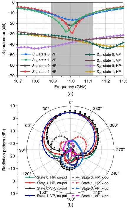
Fig.2 Simulation performance of the element: (a) Sparameter;(b) radiation pattern
The losses of the PIN diode and the designed DC bias circuit are analyzed.Because a part of the diode is equivalent to a resistance when it is turned on,there is a large resistance loss,so the loss from the PIN diode is calculated to be 0.7 dB by using the metal strip instead of the conduction diode.The simulation calculation by removing the DC bias circuit shows that the loss from the DC bias circuit is 0.66 dB,while the loss from other aspects (impedance mismatch,patch,etc.)is 0.54 dB.
To distinguish states 0 and 1 more intuitively,Fig.3 presents the current distribution of the element in the two states.It can be seen that the currents in the two states are opposite.

Fig.3 Surface current of the element in two states
This characteristic can be equivalent to logical 0 and 1,and a 2-element subarray is designed to verify the effect of different combinations of 0 and 1 on the radiation pattern (Section 2 of the supplementary materials).
3 Design of the dual-polarization and dual-beam antenna array
A 6×12 array antenna is designed to achieve dualpolarization and dual-beam scanning.To achieve realtime dynamic control of the polarization and beam of the array,a 72-channel,series-parallel,equal-amplitude,and in-phase feeding network and the corresponding DC bias circuit are designed.The structure of the feeding network printed on the bottom of substrate 2 is demonstrated in Fig.4.The feeding network primarily adopts the quarter-impedance transition from transmission line theory to achieve the current distribution ratio at the output port,and the in-phase is achieved by designing the distance between the two ports to beλg(waveguide wavelength).The feed structure adopts a grounded coplanar waveguide (GCPW).Due to the strong trunk signal of the feeding network,two rows of ground metal vias are designed on both sides of the microstrip line to suppress the leakage of the RF signal to the surroundings,thereby reducing coupling to surrounding antenna elements.
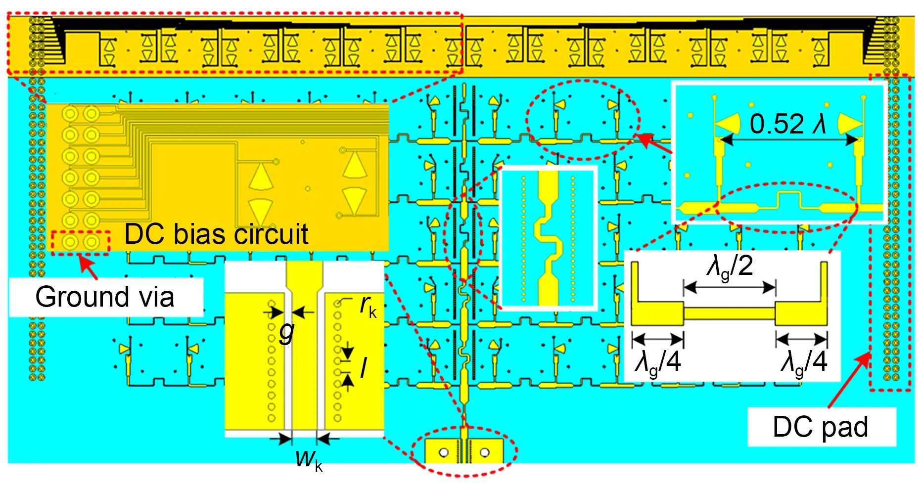
Fig.4 Structure of the series-parallel feeding network and DC bias circuit
The microstrip lines are bent to align with the spacing of the elements,as indicated in Fig.4,and the structure of the DC bias circuit is given.The array requires 144 independent I/O ports to control the states of all elements.To enable a stable control of the PIN diodes by the output voltage,ground vias are set in each row of the array to achieve the stable voltage difference.
Fig.5 shows the amplitude and phase of the simulatedS-parameters of the feeding network,whereS11less than -15 dB is at 11 GHz and the amplitudes of other ports are essentially the same.The phase difference of each output port is within 12°,which basically satisfies the equal phase requirement.

Fig.5 Simulated S-parameter and output phase of the feeding network
From the perspective of holographic theory (Johnson et al.,2015;Deng et al.,2021;Xu M et al.,2022),the antenna element is digitally encoded to verify the beam scanning capability of the antenna array.
More detailed introduction about the holographic control theory can be found in Section 3 of the supplementary materials,and based on the digital coding theory,the beam scanning characteristics of the array at 11 GHz are simulated.Fig.6 shows the far-field patterns of the array.The simulation results suggest that the array can achieve precise beam steering at the preset angle.

Fig.6 Far-field patterns corresponding to different angles
4 Prototype fabrication and measurement
To verify the performance of the proposed antenna,2-element subarray and 6×12 antenna array prototypes are fabricated and tested.In the test,the 2-element subarray is fed with a one-to-two power divider through the RF cable,with the integrated PIN diodes controlled by a DC voltage source capable of outputting±1.3 V.The PIN diodes in the 6×12 antenna array are controlled by a control board with 16×16 I/O ports based on a single-chip microcomputer,as shown in Fig.7.
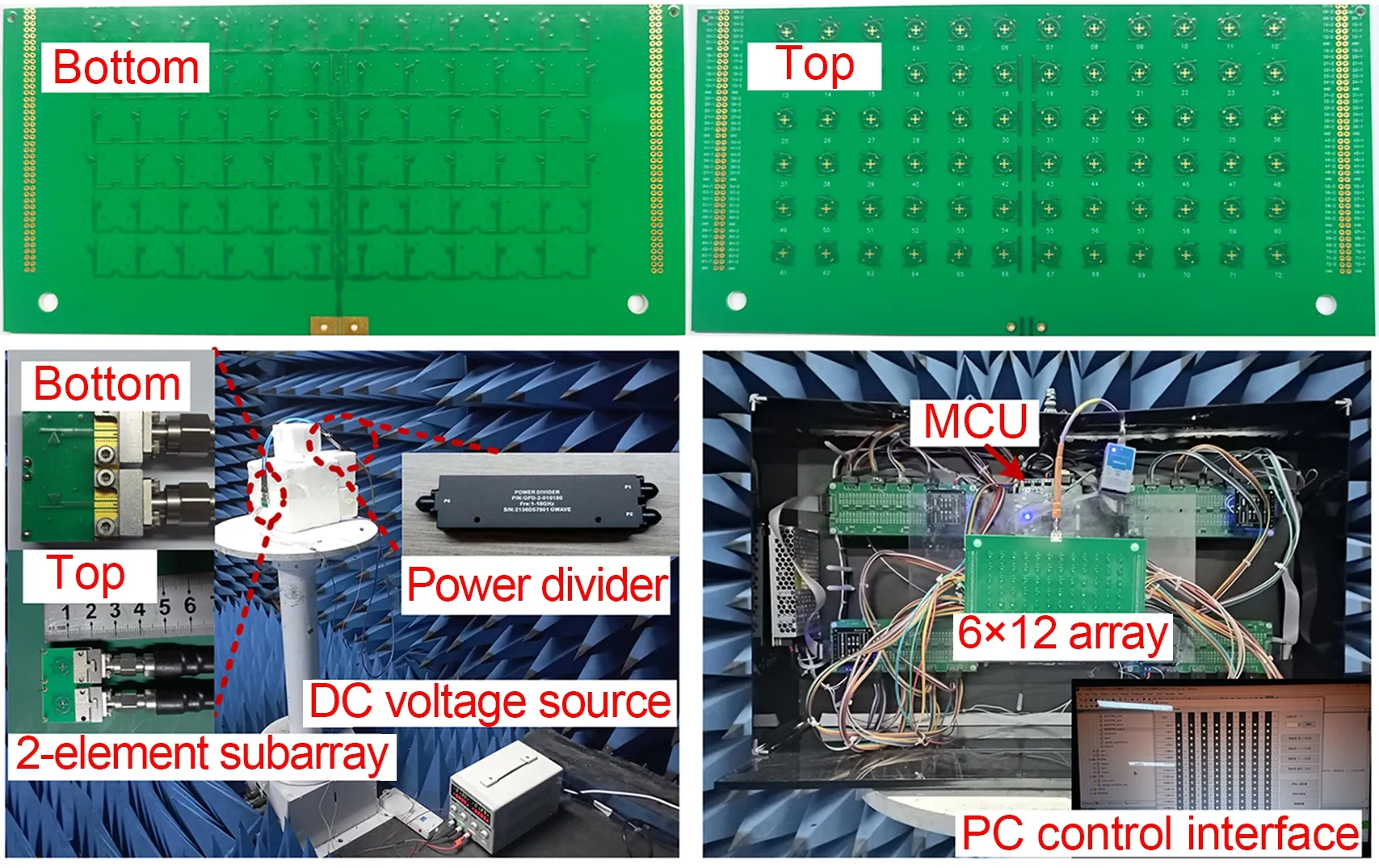
Fig.7 Photographs of the fabricated 2-element subarray,6×12 array,and environment of measurements
The measurement results of the 2-element subarray are given in Section 4 of the supplementary materials.
The measurement of the 6×12 array is shown in Fig.8.The code sequence of different deflection angles is imported into the single-chip microcomputer through the host computer,and the corresponding voltage is outputted from the extended I/O ports to control the PIN diodes;consequently,the beam deflection of the specific angle can be achieved.When ignoring the error of the antenna placement angle due to human factors,the simulation and measurement results are basically consistent,and the measured main lobe direction can be accurately deflected to the preset angle,which verifies the stable and accurate beam deflection of the proposed antenna system.
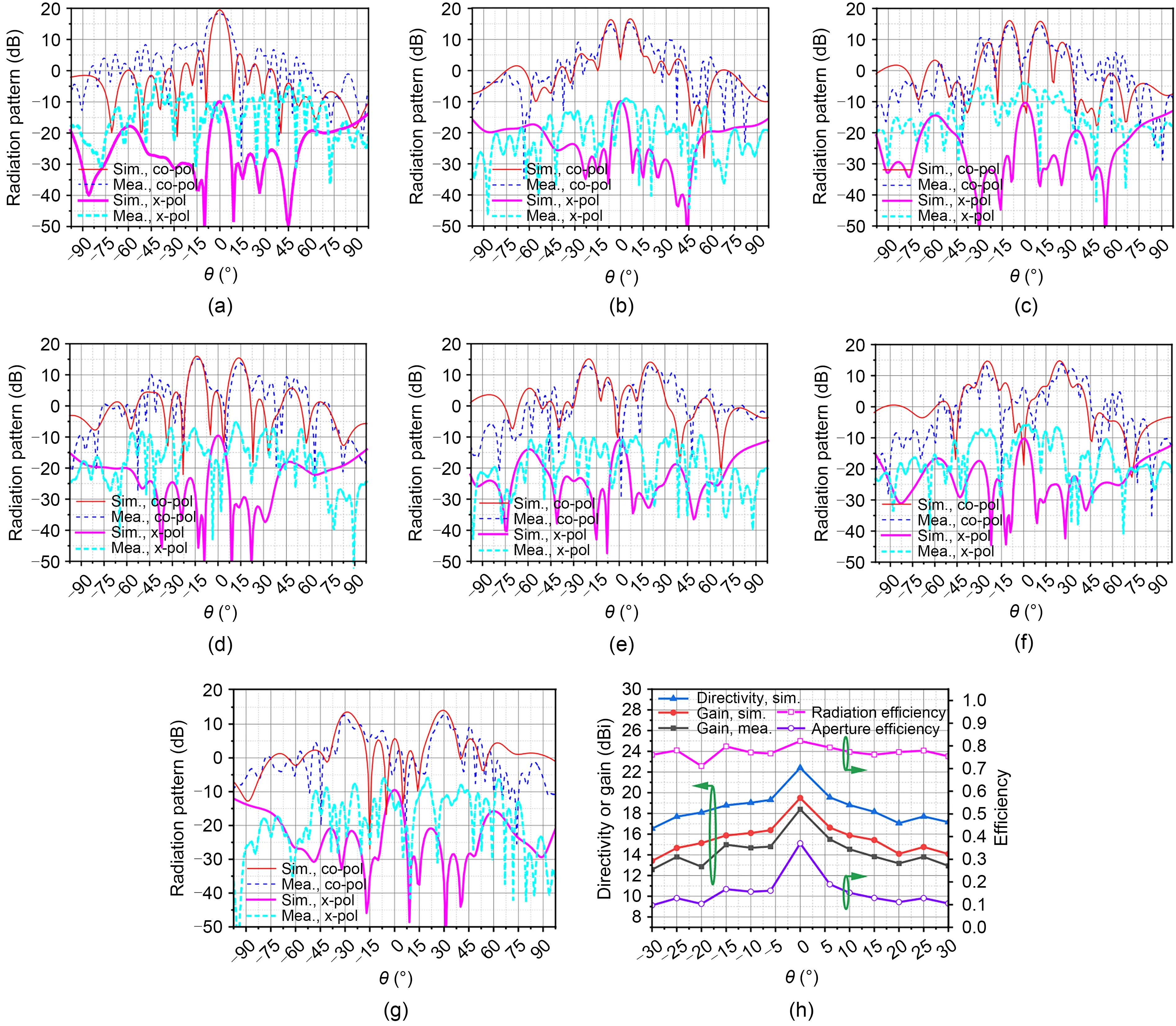
Fig.8 Simulated and measured radiation patterns (a-g) and directivity,gain,and efficiency of the 6×12 antenna array(h) at different steering angles: (a) θ0=0°,φ0=0°;(b) θ0=±5°,φ0=0°;(c) θ0=±10°,φ0=0°;(d) θ0=±15°,φ0=0°;(e) θ0=±20°,φ0=0°;(f) θ0=±25°,φ0=0°;(g) θ0=±30°,φ0=0°
Moreover,the cross-polarization of the dualpolarization antenna array is lower than -20 dB.However,the measured radiation pattern suffers from problems such as high-side lobe level and a little jitter in the main lobe,which may be caused mainly by the resonant frequency shift and the random phase difference introduced by the manufacture of the feeding network.In addition,the feeding network adopted in this study has equal amplitude at each port,and has an inherently high-side lobe level when used in the array antenna.Sidelobe performance can be improved by increasing the number of elements or using unequal amplitude feeding.
The simulated directivity and gain and measured gain and efficiency of the antenna system are shown in Fig.8h.Here,the measured efficiency is the ratio of the measured gain to the simulated directivity.The results suggest that the radiation efficiency at each scanning angle is >70%.Because of the shift of the resonant frequency and the loss of the feeding network,PIN diodes,and DC bias circuit,the measured gain is reduced to a certain extent.The maximum aperture efficiency is 37% at 0°.The aperture efficiency is low at other angles because the gain decreases rapidly with the increase of the scanning angle.The main reasons for the decrease in gain are as follows:First,the proposed antenna array has symmetrical dual beams except for the 0° direction;compared with the single beam in the 0° direction,the symmetrical dual beam peak value is reduced by 3 dB (the energy is divided into two parts).Second,the antenna element has only two-phase radiation states,that is,1-bit phase quantization,and the phase accuracy is low,which will lead to quantization loss.
A comparison with other antennas is given in Table 2.Most of the 1-bit beam scanning arrays proposed in recent years are reflection or transmission arrays,which are characterized by a high profile due to the need for a primary feed in space.In addition,there are few reports about the 2D radiation-type beam scanning antenna,and all of them are single polarization.In contrast,our antenna array features a low profile,dual-polarization,dual-beam,and a beam scanning step angle of 5° to ensure gain.

Table 2 Comparison between the proposed beam scanning antenna and other reported antennas
5 Conclusions
In this paper,a dual-polarization dual-beam scanning array antenna based on holographic control theory is proposed.The antenna element integrates four PIN diodes,two in each of the horizonal and vertical directions,to achieve reconfigurable polarization.By varying the states of two PIN diodes in the same direction to change the radiation phase of the element,the simulation and measurement of the 2-element subarray verify that the proposed element is capable of manipulating the radiation pattern.Based on digital coding theory,the phase-adjustable structure integrated with the PIN diodes can act as a holographic element,and the desired object wave can be accurately and stably obtained by modulating the reference wave excited by the feed and the holographic element.The simulation verifies that the antenna array can achieve satisfactory 2D beam scanning.To verify the simulation results,a 2-element subarray prototype and a 6×12 array prototype are fabricated and subjected to measurement.The results of measurement and simulation are in good agreement,which proves the feasibility of the dual-polarization dual-beam scanning antenna system.Due to its low profile,low cost,and easy integration,this antenna system excels in applications in fields such as radar systems and smart antennas.
Contributors
Shichao ZHU designed the research.Shichao ZHU,Yuanfan NING,and Hongbo CHU tested the antenna system.Shichao ZHU drafted the paper.Pei XIAO helped organize the paper.Shichao ZHU and Gaosheng LI revised and finalized the paper.
Compliance with ethics guidelines
Shichao ZHU,Yuanfan NING,Hongbo CHU,Pei XIAO,and Gaosheng LI declare that they have no conflict of interest.
Data availability
The data that support the findings of this study are available from the corresponding author upon reasonable request.
List of supplementary materials
1 Supplement to the analysis of the element
2 Supplement to the analysis of the 2-element subarray
3 Supplement to the holographic control theory
4 Supplement to the measurement results of the 2-element subarray
杂志排行

Frontiers of Information Technology & Electronic Engineering的其它文章
- Correspondence:Uncertainty-aware complementary label queries for active learning∗
- Path guided motion synthesis for Drosophila larvae*#
- Wideband and high-gain BeiDou antenna with a sequential feed network for satellite tracking
- Synchronization transition of a modular neural network containing subnetworks of different scales*#
- RFPose-OT:RF-based 3D human pose estimation via optimal transport theory∗
- Attention-based efficient robot grasp detection network∗