Multilevel optoelectronic hybrid memory based on N-doped Ge2Sb2Te5 film with low resistance drift and ultrafast speed
2023-11-02BenWu吴奔TaoWei魏涛JingHu胡敬RuiruiWang王瑞瑞QianqianLiu刘倩倩MiaoCheng程淼WanfeiLi李宛飞YunLing凌云andBoLiu刘波
Ben Wu(吴奔), Tao Wei(魏涛), Jing Hu(胡敬), Ruirui Wang(王瑞瑞),Qianqian Liu(刘倩倩), Miao Cheng(程淼), Wanfei Li(李宛飞),Yun Ling(凌云), and Bo Liu(刘波),2,§
1Suzhou Key Laboratory for Nanophotonic and Nanoelectronic Materials and Its Devices,School of Materials Science and Engineering,Suzhou University of Science and Technology,Suzhou 215009,China
2State Key Laboratory of Functional Materials for Informatics,Shanghai Institute of Microsystem and Information Technology,Chinese Academy of Sciences,Shanghai 200050,China
Keywords: multilevel optoelectronic hybrid memory, N-doped Ge2Sb2Te5 thin film, low resistance drift, ultrafast speed
1.Introduction
With the era of big data is coming and the data amount will reach more than 175 ZB in the year of 2025.[1]There is a great demand to increase storage capacity and density,where multilevel memory is an efficient method to address the above-mentioned issues.Among all kinds of memories, phase-change memory (PCM) is emerging as an attractive technology owing to its high-speed, scalable and nonvolatile characteristics.[2]The principle of PCM is that an electrical pulse is utilized to achieve the resistance changes by reversible phase transformation characteristics and thus data recording/erasing.In PCM,SET operation is defined that the initial amorphous phase(high resistance)is transformed into a crystalline state (low resistance) by applying a wide/multiple electrical/laser pulse with moderate intensity(sufficient to heat the film above the phase-transition temperature,but lower than the melting temperature).RESET operation is defined that the crystalline state(low resistance)is transformed into an amorphous state (high resistance) via the narrow electrical/laser pulse with high intensity to melt the phase-change film.Finally, the information is read out by measuring the resistance change of phase change materials.Fortunately,the resistance ratio of amorphous to crystalline phases is as high as several orders of magnitude,[3]allowing intermediate resistance states to be realized, which is beneficial for storing multiple bits of data in a single memory cell.Thus, its storage capacity increases exponentially without changing the physical volume and the memory cost per bit is dramatically reduced.Therefore, PCM may provide a promising solution for multilevel storage because of its low-cost, low power consumption and multiple resistance states.[4]
However, the SET/RESET operation based on electrical pulse is a pure thermal process and difficult to balance the contradiction between thermal stability and operation speed.Although the operation speed of PCM can be as fast as 700 ps or even 242 ps,where the operation speed is defined as the minimum pulse duration required to induce a given phase transformation, its ten-year data-retention is still poor.[5,6]On the other hand, when the thermal stability of PCM is improved and the ten-year data-retention temperature increases, its operation speed will decrease significantly because the improvement in thermal stability of phase change materials will make the crystallization process more difficult.For example,in Rudoped Sb2Te-based PCM,the ten-year data-retention temperature reaches 143°C, however, the SET speed is as slow as 6000 ps.[7]Interestingly, the laser pulse width as short as picosecond/femtosecond scale has been utilized to perform reversible phase transformation between amorphous and crystalline states.[8,9]The ultrashort laser pulse provides a powerful tool combining thermal processes and photon effects to achieve fast SET/RESET operation speed in PCM.Therefore, the combination of ultrafast laser writing and resistance readout is a more promising method to realize the ultrafast SET/RESET operation and multilevel memory.Thus,the concept of optoelectronic hybrid phase-change memory (OEHPCM)is proposed.
To achieve ultrafast multilevel OEH-PCM, appropriate phase change material is indispensable.Ge2Sb2Te5(GST)thin film,as a typical phase change material,has been widely investigated for multilevel storage due to its high resistance contrast and the rapid reversible transformation between the crystalline and amorphous phases.[10-12]However, its low thermal stability (ten-year data retention temperature of only 87°C[13]) restrains the storage application in high temperature environment while its high resistance drift(coefficient of 0.17[14]) will cause the merging of intermediate states during multilevel memory and thus lead to undesired bit errors.Doping engineering is a simple and effective method to improve the intrinsic properties of GST thin films.So far,various doping elements have been proposed to enhance the comprehensive properties of GST,such as Cr,[15]Sc,[13]C,[16]N,[17]Nb,[18]W,[19,20]Sm,[21]Al,[22]Si,[23]Ti,[24]and so forth.[25]Among others, N doping is a promising selection to enhance the resistance of amorphous and crystalline GST film as well as its thermal stability.[26-28]Its resistance ratio of amorphous to crystalline state is higher than two orders of magnitude under SET/RESET operation, however, the operation speed is reported only several hundreds of nanoseconds.[28]Therefore,it is necessary to further improve the comprehensive performance by optimizing the N-doping amount.
In this work, the thermal stability and resistance drift of N-doped GST (NGST) thin films are investigated.The multilevel memory performances of NGST-based OEH-PCM are analyzed and the structural evolution is further elucidated.This work may provide a useful reference for investigating the ultrafast multilevel phase change memory.
2.Experimental details
NGST thin films with the thicknesses of 200 nm are deposited onto Si substrate by magnetic co-sputtering method,where the sputtering power of GST target is 80 W and the N-doping content is adjusted by controlling the Ar/N2flow ratio of 40/2,40/4,and 40/6,respectively.The working pressure is 0.8 Pa and sample is rotated at 15 r/min to keep uniform film composition and thickness.The N concentrations are 20.8 at.%, 27.4 at.%, and 29.8 at.%, respectively, by energy dispersive spectrometry analysis.The dependence of resistance on temperature (R-Tcurve) is tested at N2gas protection and the heating rate of 30°C/min.The combination of resistance tester (KEITHLEY 2450) and heating platform (LINKAM HFS600E-PB4) is utilized to obtain theRTcurves, failure time and resistance drift characteristics of NGST thin films.Picosecond laser induced crystallization is analyzed by transmission electron microscopy(TEM,type:Tecnai G2 F20 S-TWIN)to elucidate the multilevel resistance states, where the NGST film with 20-nm thickness is firstly deposited on a copper mesh with a diameter of 2 mm attached with a carbon supporting film by magnetron sputtering.The binding environment of NGST thin film is characterized via x-ray photoelectron spectroscopy (XPS, Thermo ESCALAB 250XI)to understand the improved thermal stability.The oxide layers of all film surfaces are removed by Ar+bombardment before XPS measurement.During the measurement,AlKαray with the energy of 1486.6 eV and beam spot of 400µm is adopted.The scanning pass energy is 50 eV with the step of 0.1 eV and the scanning numbers of 5.All characteristic peaks of XPS spectra are calibrated by standard C 1s peak at 284.8 eV.
The memory unit is fabricated as follows: NGST film with the thickness of 50 nm is deposited on the T-type bottom electrode (fabricated by CMOS process), and ITO electrode film with the thickness of 10 nm is deposited onto the NGST layer as a protection film and top electrode.The phase change materials and ITO electrodes are patterned by optical lithography and subsequent etching methods.The OEH-PCM testing system is further built to measure the memory performance,where picosecond laser(the laser wavelength of 532 nm,half maximum pulse width of 13 ps,repetition frequency of 10 Hz and spot diameter of 1 mm)is applied to stimulate reversible phase transition of NGST thin films,and Keithley’s 4200 electrical testing module is adopted to collect resistance signals.When picosecond pulse is illuminated into the region of ITO electrode and NGST film,the resistance is measured by probe contacting the bottom W electrode and top ITO electrode.
3.Results and discussion
Figure 1(a) shows the dependence ofR-Tcurves in NGST thin films.The relationship of phase-change temperature (Tc) and N concentration is also plotted in the inset of Fig.1(a).It is noted that theTcis defined the minimum value after the derivative of the resistance to temperature(dR/dT).[29]One can see that the increment of temperature results in the gradual reduction of resistance at each N concentration due to the semiconductor behavior.The sudden reduction of resistance can be ascribed to the phase-change process.With increasing N content,Tcgradually increases from 171°C to 259°C,revealing the enhanced thermal stability.To evaluate the data-retention ability after N doping,figure 1(b)shows the Arrhenius fitting plots of NGST films obtained by Arrhenius equation.[20]When the initial resistance reduces to its half value at a given temperature, the required time is defined as the failure time.Results show that all NGST thin films possess excellent ten-year data-retention temperature (T10-year),much higher than those of pure Ge2Sb2Te5(T10-year=92°C),Sc-doped Ge2Sb2Te5(T10-year = 119°C),[13]Zn1.25Sb2Te3(T10-year = 105°C),[30]and Sb2Te (T10-year = 55°C).[3]In addition, theT10-year of NGST film gradually increases from 125°C to 191°C with increasing N concentration, implying that N doping is very favorable for enhancing data-retention ability of GST thin film.When the N concentration is 27.4 at.%, theT10-year reaches 175°C, which is sufficient to meet the long-term data storage requirements of consumer electronics(T10-year=85°C),vehicle chip(T10-year=120°C),and military electronics(T10-year=150°C).[15,31]
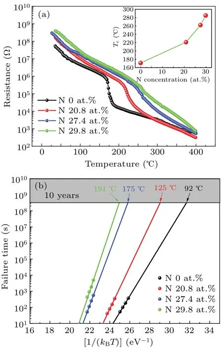
Fig.1.(a) Dependence of resistance on temperature at the heating rate of 30 °C/min, (b) Arrhenius fitting plots of NGST films to evaluate the dataretention ability.
The SET/RESET and reversible switching endurance performances of NGST film and corresponding memory device were further investigated.Figures 2(a)and 2(b)show the dependence of the film resistance on the laser fluence and pulse width during SET operation,respectively.It can be seen from Fig.2(a) that for NGST films with different N contents, the resistances all decrease with the increment of laser fluence at a given pulse width.This is due to the higher laser fluence leading to the increment of crystallization degree.When the N concentration is 0 at.%, the resistance ratio can reach three orders of magnitude at the pulse width of 130 ps and energy fluence of 0.14 mJ/cm2.However, the reduction amplitude of resistance becomes smaller and the required laser pulse width and laser fluence become larger with increasing N concentration.For instance, the resistance ratio with N concentration of 27.4 at.%reduces to two orders of magnitude at the pulse width of 780 ps and fluence of 1.91 mJ/cm2while only one order of magnitude can be obtained at the N concentration of 29.8 at.% with the pulse width of 780 ps and fluence of 2.34 mJ/cm2.In Fig.2(b),the similar situation can be observed.The resistance decreases with increasing pulse width at a given N concentration and laser fluence.It can also be explained that the contribution of laser fluence and pulse to crystallinity can be equivalent at a certain extent.The wider pulse and higher fluence both generate more energy to achieve higher crystallinity in NGST film.It can be found that the SET operation of pure GST thin film can be completed at 52 ps along with the resistance ratio as high as three orders of magnitude.With increasing the N concentration to 20.8 at.%and 27.4 at.%,the SET operation speed can be as fast as 390 ps and 520 ps, respectively, together with the resistance ratio of two orders of magnitude.However, the low resistance ratio of only one order of magnitude is obtained at the pulse width of 520 ps when the N concentration reaches 29.8 at.%.The increment of pulse width and laser fluence required to induce low resistance state with increasing N concentration can be ascribed to the enhanced thermal stability by N doping.In a word, the NGST thin film with the optimal N concentration of 27.4 at.%has the fast SET speed of 520 ps as well as large resistance ratio of two orders of magnitude.It is noted that picosecond laser could induce ultrafast phase transition rather than electrical pulse,which may be explained that laser pulse waveform is better,and energy density is higher.In addition to thermal effect, there are also parts of photon effects to induce phase transition, while only thermal effect exists in electrical pulse.[32]Figure 2(c)shows the relationship between the resistance and the laser fluence at the pulse width of 13 ps for RESET operation.The resistance increases with the laser fluence at each N concentration, which is induced by the higher amorphous degree at larger laser fluence.The resistance ratio is reduced from three orders of magnitude to one order of magnitude when the N concentration is increased from 0 to 29.8 at.%.It is well known that high resistance ratio is very helpful to implement good signal-to-noise ratio in data recording and readout.Thus,the NGST thin film with N content of 27.4 at.% is a promising candidate due to its fast RESET speed (13 ps), high resistance ratio (two orders of magnitude) and superior data-retention ability (T10-year =175°C).In this case,the reversible switching endurance characteristics of corresponding device are obtained in Fig.2(d),suggesting reversible switching was realized with the resistance ratio of two orders of magnitude.Due to the imperfection of the testing system, it is necessary to manually complete the SET/RESET operation, and the testing efficiency is extremely low.The number of cycles that can be tested is also very limited and the device fabrication process also needs to be further improved to obtain better fatigue properties.Nevertheless,it is still proved that NGST thin film is a promising phase change material for OEH-PCM with ultrafast operation speed and data-retention.
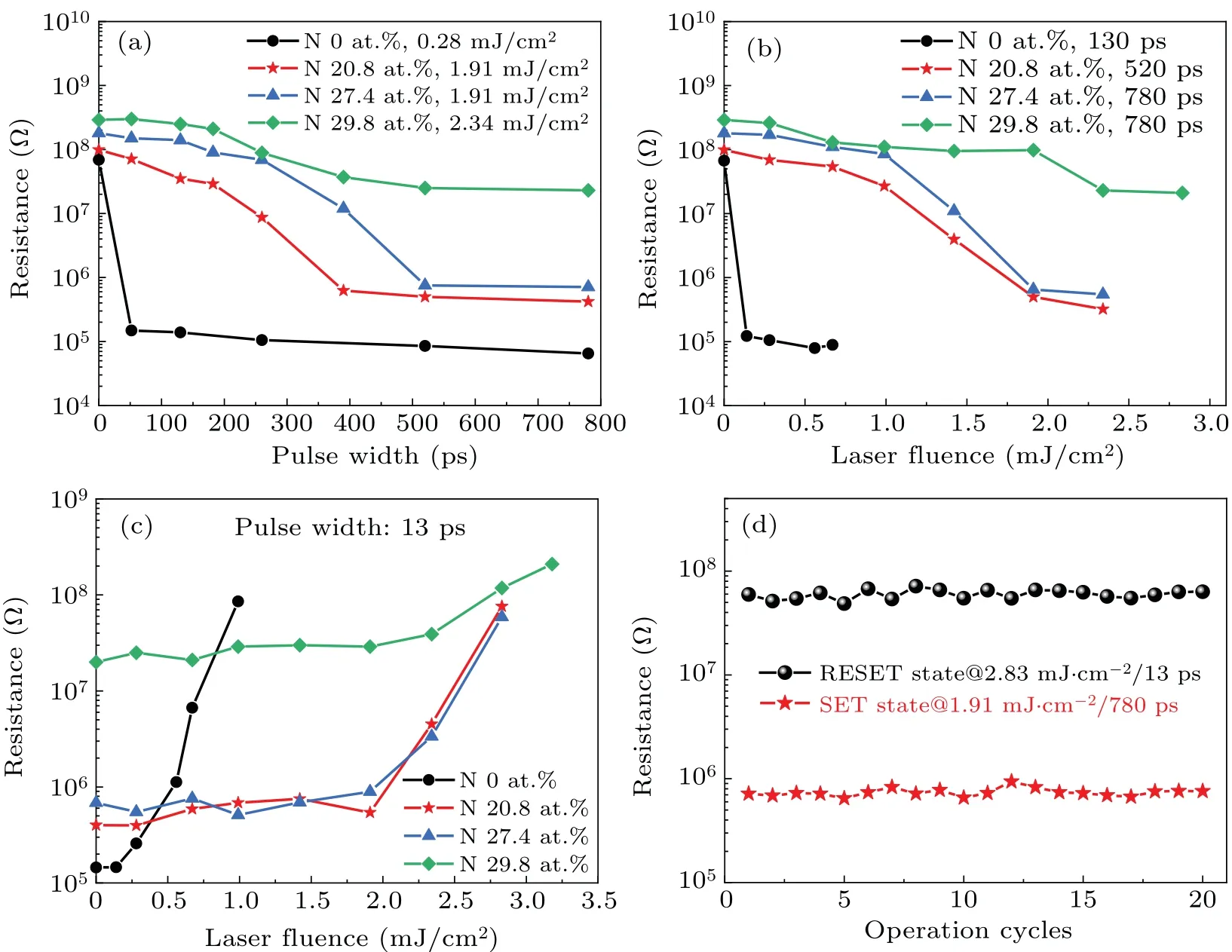
Fig.2.Dependence of resistance on(a)laser fluence,(b)pulse width for SET operation; (c)dependence of resistance on laser fluence at the single pulse for RESET operation;and(d)reversible switching endurance characteristics of NGST-based device with N content of 27.4 at.%
The NGST thin film with N content of 27.4 at.%is further used to estimate the multilevel OEH-PCM performance, as shown in Figs.3(a)and 3(b),where the SET laser pulse width is fixed at 520 ps with various fluences and RESET pulse width is 13 ps at the laser fluence of 2.83 mJ/cm2.Figure 3(a)indicates the resistance is reduced from 5×10⁸Ω (namely, level 1) to 1×10⁸Ω (namely, level 2) with large resistance ratio of five times when the energy fluence is 0.99 mJ/cm2, as the first SET operation(SET 1).The further increment of fluence to 1.42 mJ/cm2results in the reduced resistance to 1×10⁷Ω(namely,level 3)with the resistance ratio of level 2 to level 3 of ten times, as the second SET operation (SET 2).When the laser energy reaches 1.91 mJ/cm2,the resistance is further reduced to 1×10⁶Ω (namely, level 4) with large resistance ratio of level 3 to level 4 of also ten times, as the third SET operation(SET 3).Besides,each level at laser irradiation has stable resistance,beneficial for accurate multi-bit data storage.Figure 3(d) shows that the resistance at each level can be returned to the high resistance initial state when the laser fluence reaches 2.83 mJ/cm2with the pulse width of 13 ps.Therefore,NGST thin film can realize ultrafast multilevel SET/RESET operation.
The resistance as a function of time can be expressed asR=R0(t/t0)ν, whereR0is the initial resistance at timet0andνis the resistance drift coefficient.[33]The linear fitting on resistance as a function of time is plotted in Figs.3(c)and 3(d)to obtain the resistance drift for evaluating the resistance stability.Figure 3(c) reveals the very lowν(0.00024)at 85°C,0.00170 at 120°C,0.00249 at 150°C,much lower than those of GeTe film(~0.4)with the thickness of 100 nm at 85°C,[34]and AgInSbTe film (~0.061) with thickness of 15 nm at 30°C,[35]suggesting that NGST thin film has great potential in consumer electronics, vehicle chip, and military electronics.[15]The reduced resistance drift in NGST thin film is explained that the formation of strong Ge-N bonds increases the rigidity of the network.[35,36]In the multilevel storage,the high resistance stability of each level is beneficial for achieving accurate data recording and readout.In Fig.3(d),one can see the resistance drift coefficients of level 2,level 3,and level 4 are as low as 0.00005, 0.00652, and 0.05775, respectively.It is noted that when the resistance of NGST film reduces to the lower value, the resistance drift coefficient will increase obviously.Resistance drift is closely related to the structural relaxation process of thin film.The elevated laser fluence will accelerate the structural relaxation and leads to the increment of resistance drift coefficient.[37]In addition,higher laser fluence causes not only the higher crystallization degree but also more defects induced by inner stress, which is mainly due to the increased volume shrinkage of phase change materials as the crystallinity increases.But even so,the resistance drift of NGST is still very low compared with other reports (0.017,0.076, and 0.092, respectively, in Ge-Ga-Sb film at room temperature).[38]Thereby,NGST thin film with low resistance drift is advantageous for performing reliable multilevel OEHPCM.
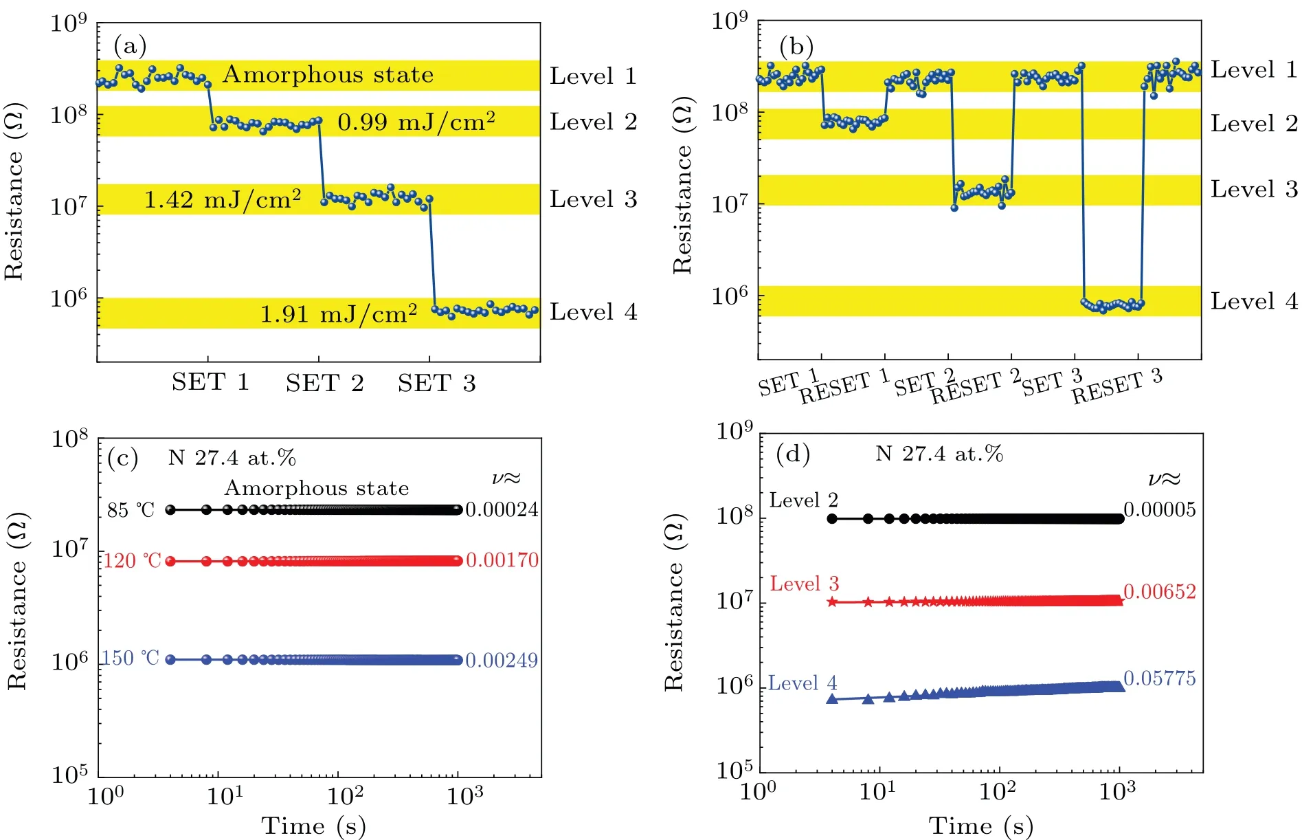
Fig.3.(a)Dependence of SET resistance on different laser fluences at 520 ps; (b)SET/RESET operation of multilevel resistance switching;(c)resistances of RESET or amorphous state at different temperatures as a function of time;(d)resistances at different levels as a function of time,where the laser is turned off after laser irradiation.The N concentration is fixed at 27.4 at.%for NGST thin film.
In order to elucidate the multilevel memory phenomenon,figure 4 shows the TEM images of the NGST films at different laser fluences, where the N concentration is 27.4 at.%.Figures 4(a), 4(c), and 4(e)indicate the higher crystallization degree and larger grain size with increasing the laser energy from 0.99 mJ/cm2to 1.91 mJ/cm2, corresponding to the resistance states at levels 2, 3, and 4, respectively.At the same time,the high-resolution TEM(HRTEM)images in Figs.4(b),4(d), and 4(f) all show the single face-centered-cubic crystalline phase in NGST film,indexed at(200)and(111)crystal planes.Therefore, it is concluded that the multilevel resistance states are realized by tuning crystallization degrees with the same crystalline phase.
In order to understand the bonding changes of NGST films under different laser fluences, where the N concentration is 27.4 at.%,XPS analyses of Ge,Sb,Te,and N elements are performed,as shown in Fig.5.Gaussian fitting is also performed to obtain concrete peaks.For the as-deposited NGST film (Fig.5(a)), the Ge 3d5/2, Sb 4d5/2, and Te 4d5/2peaks are located at higher 31.1 eV, 32.7 eV, and 40.4 eV, respectively, while the binding energies of Ge 3d5/2, Sb 4d5/2, and Te 4d5/2levels in pure GST film are located at lower 29.6 eV,32.3 eV,and 40.0 eV,respectively.[39]It is well known that the electronegativity of N atom is 3.0, much higher than those of Ge (1.8), Sb (1.9), and Te (2.1) atoms.[17]When the bonded atoms are replaced by the atoms with higher electronegativity,the binding energy will rise.Thus,the increased binding energies in NGST film are ascribed to the formation of Ge-N,Sb-N, and Te-N bonds, which can be further confirmed by N 1s spectra in Fig.5(b),where the N 1s peak at 397.4 eV is due to the nitride formation.[39]The nitride formation in NGST film is beneficial for enhancing the thermal stability,weakening the structural relaxation and thus the lower resistance drift.
When NGST film is irradiated by the laser fluence of 0.99 mJ/cm2,the binding energies are all shifted toward higher direction.This is because that the“wrong bonds”such as Ge-Ge,Sb-Sb,and Te-Te bonds existed in the as-deposited state are gradually broken and the Ge-Te,Sb-Te bonds and nitride with higher binding energy are further generated via the phase transition.When the fluence is increased to 1.42 mJ/cm2,the binding energies are all slightly shifted to lower direction.This is due to that parts of N-Ge, N-Te, and N-Sb bonds existed in the deposited-state begin to be broken, and the bond rearrangement occurs, resulting in the formation of Ge-Te and Sb-Te bonds with slightly lower binding energy.The excess N will combine with Sb to form a new N-Sb bond instead of the original N-Te bond, which is well illustrated by the reduced binding energy of N 1s level in Fig.5(b).However,the increment of fluence to 1.91 mJ/cm2results in the larger binding energies in Ge 3d5/2,Sb 4d5/2,and Te 4d5/2levels due to the further increment of structural order and the formation of more nitride.
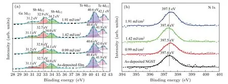
Fig.5.XPS spectra of(a)Ge 3d, Sb 4d, and Te 4d; (b)N 1s core-levels, where Gaussian fitting is performed to obtain concrete peaks.The solid line represents the fitting results while the dash line represents raw data.
4.Conclusion
In summary, NGST is proposed to achieve multilevel OEH-PCM with excellent thermal stability and fast operation speed.Results show that when N content is 27.4 at.%, the NGST can make the phase transition temperature up to 260°C and the ten-year data retention temperature up to 175°C.The SET operation speed of NGST thin film can reach 520 ps while the RESET operation speed can reach 13 ps.Meanwhile,the NGST based memory device can implement good reversible switching cycle accompanied by the large resistance ratio of two orders of magnitude.The multilevel storage investigation indicates NGST film can realize four reversible resistance states with very low resistance drift coefficients and large resistance ratio at the operation speed of 520 ps.Structural analysis implies that multiple resistance states are due to the various crystallization degree of NGST films and the existence of nitrides is favorable for improving the thermal stability.
Acknowledgements
Project supported by the National Natural Science Foundation of China (Grant Nos.62205231 and 22002102), the Postgraduate Research & Practice Innovation Program of Jiangsu Province, China (Grant No.KYCX223271), and Jiangsu Key Laboratory for Environment Functional Materials.
杂志排行
Chinese Physics B的其它文章
- Corrigendum to“Reactive oxygen species in plasma against E.coli cells survival rate”
- Dynamic decision and its complex dynamics analysis of low-carbon supply chain considering risk-aversion under carbon tax policy
- Fully relativistic many-body perturbation energies,transition properties,and lifetimes of lithium-like iron Fe XXIV
- Measurement of the relative neutron sensitivity curve of a LaBr3(Ce)scintillator based on the CSNS Back-n white neutron source
- Kinesin-microtubule interaction reveals the mechanism of kinesin-1 for discriminating the binding site on microtubule
- Investigation of Ga2O3/diamond heterostructure solar-blind avalanche photodiode via TCAD simulation
