Novel layout design of 4H-SiC merged PiN Schottky diodes leading to improved surge robustness
2023-10-11JiaHaoChen陈嘉豪YingWang王颖XinXingFei费新星MengTianBao包梦恬andFeiCao曹菲
Jia-Hao Chen(陈嘉豪), Ying Wang(王颖),†, Xin-Xing Fei(费新星), Meng-Tian Bao(包梦恬), and Fei Cao(曹菲)
1College of Electronics and Information,Hangzhou Dianzi University,Hangzhou 310018,China
2The Yangzhou Marine Electronic Instrument Institute,Yangzhou 225001,China
Keywords: merged PiN Schottky(MPS)diode,silicon carbide(SiC),surge capability,surge energy,reliability
1.Introduction
Silicon carbide (SiC) is a third-generation semiconductor material that has become widely used in the preparation of high-voltage, high-temperature, high-power, irradiationresistant power electronics devices due to its excellent material properties, such as a wide bandgap, high critical breakdown electric field and high thermal conductivity.[1–3]During application, SiC power devices may experience lightning strikes,short circuits and the occurrence of momentary high-current pulses,which will exceed the rated current value of the device,causing the device to experience brief high-current conditions.Therefore,surge capability is an important factor in assessing the reliability of power devices.[4,5]
The resistance to a surge current refers to the ability of a device to withstand large current pulses under forward-bias conditions.According to previous studies, during the surge process, large current pulses flow through the device, generating a corresponding voltage drop.Such a voltage drop generates a large heating power, causing the temperature of the device to rise sharply in a short period of time, which may eventually make the anode metal of the device melt,leading to device failure.[6–8]Therefore,the main method for improving the surge capability of a device is to limit the rise in temperature of the device junction.
Merged PiN Schottky(MPS)diodes contain both a Schottky junction and a p–n junction.MPS diodes combine the advantages of the low forward voltage drop and short reverse recovery time of Schottky diodes with the small reverse leakage current of PiN diodes.[9]When the forward voltage is small,only the Schottky junction is turned on,majority carriers flow through the device and the MPS diode is in the unipolar operating mode.As the positive voltage increases,the built-in P–N junction is turned on,and a large number of holes are injected into the drift region, which reduces the on-resistance of the device.At this time,the device works in the bipolar operating mode.[10–14]
This study proposes a novel layout design to improve the surge capability of 4H-SiC MPS diodes and uses Silvaco technology computer-aided design (TCAD) software to perform three-dimensional(3D)electro-thermal simulations of the device.The results show that by designing a continuous P+surface (CPS), the bipolar on-voltage of the MPS diode can be reduced so that it enters the bipolar operating mode earlier during the surge process.The P+ regions are connected to each other over the entire surface of the device;thus,the current and temperature distributions on the surface of the device are uniform, which reduces heat accumulation.In addition,the structure proposed in this work does not require additional process steps to be compatible with the traditional manufacturing process of MPS diodes.
2.Device structure and simulation models
2.1.Structural parameters of the device
Figures 1(a) and 1(b) show the anode layouts of a traditional MPS diode and a MPS diode with a CPS (CPS-MPS),respectively.From Fig.1(b), it can be seen that the Schottky contact of the novel designed layout structure is composed of a uniform rectangular array,and all other areas are P+regions,which form ohmic contacts with the anode.Under normal operating conditions, the Schottky contact consisting of one of these rectangular regions conducts current,and the continuous P+region conducts a bipolar current when the P–N junction is turned on.For this new design,once the bipolar conduction is activated only in a certain P–N junction,the conducted plasma will rapidly diffuse across the entire P–N junction,thereby ensuring the uniformity of the surface current of the device and avoiding the random appearance of hotspots.Figures 2(a)and 2(b) show the simulated 3D cell structures of the traditional MPS diode and the CPS-MPS diode,respectively.Except for the different anode layout and epitaxial layer thickness, all other parameters of the two structures are the same.Table 1 shows the specific structural parameters of the devices.

Fig.1.Schematic views of (a) a MPS diode and (b) a CPS-MPS diode(blue regions are P+regions and gray ones are Schottky contact regions).
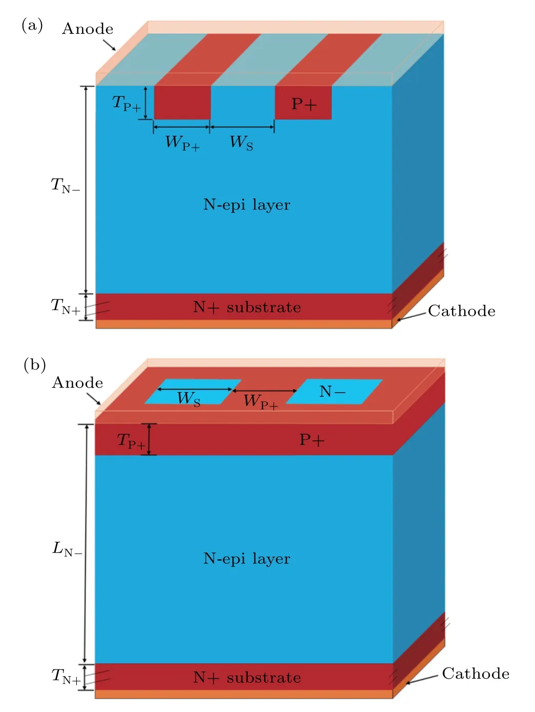
Fig.2.Three-dimensional simulation of the cell structure of (a) a MPS diode and(b)a CPS-MPS diode.
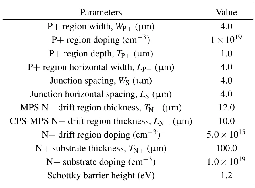
Table 1.Device parameters of a MPS diode and a CPS-MPS diode.
2.2.Device simulation models
In order to obtain realistic and reliable simulation results,this work uses 3D hybrid-circuit electro-thermal simulations to analyze the surge process of the device.During the surge process, a large amount of joule heat is generated when a high current passes through the device,and the device junction temperature increases correspondingly.[15,16]In the simulation process,the Atlas software package calculates the heat distribution of the device by solving the heat flow simulation.[17,18]The heat flow equation has the form
whereCis the heat capacitance per unit volume,κis the thermal conductivity,His the heat generated andTLis the local lattice temperature.
The main thermal parameters of SiC MPS diodes include the thermal resistance and thermal capacity.The junction temperature of a SiC MPS diode has a considerable influence on the forward conduction characteristics and reverse blocking characteristics of the device.Compared with the cathode,the thermal conductivity of the anode is very small, so the heat loss of the anode is relatively low and the heat is mainly concentrated in the cathode.Therefore,in the electrothermal simulations a thermal contact is added under the cathode and the thermal resistance is set to 0.02 K·cm2·W-1.[12,19]
Figure 3(a)shows the simulation circuit of the surge current used in this study.A half-sine current pulse with a pulse width of 10 ms(as shown in Fig.3(b))is applied to the anode of the device under test.[20]Figure 3(c)shows the temperature distribution of the cross section A–A′of the simulation cell of the CPS-MPS diode at 5.4 ms during the surge process.The device exhibits its maximum temperature near the anode surface,which would cause the anode metal(Al)to melt,leading to device failure.[8,21]This phenomenon is consistent with the experimental results,which proves the reliability of the simulation models adopted in this study.
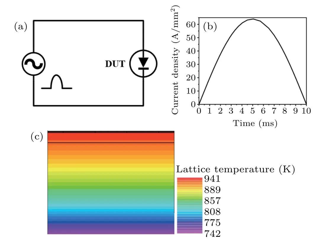
Fig.3.(a) Surge current simulation circuit, and (b) half-sine surge current pulse with a pulse width of 10 ms.(c) Temperature distribution of the CPS-MPS diode simulation cell(A–A′ cross section)at t=5.4 ms.
3.Simulation results and discussion
In this section,the simulation results of the static and dynamic characteristics of the device are presented.The simulation results prove that, compared with a traditional 4H-SiC MPS diode, the CPS-MPS diode has a lower bipolar conduction voltage and a more uniform current distribution.More importantly, the surge capability of the CPS-MPS diode is stronger and can withstand the impact of a higher current density.
3.1.Basic electrical characteristics
Figure 4 shows the forward and reverseI–Vcharacteristics of a MPS diode and the CPS-MPS diode.Figure 4(a)shows theI–Vcurves in both the low-current region and the high-current region.The forward conduction voltages of the 4H-SiC MPS and 4H-SiC CPS-MPS diodes at a rated current density ofJF=200 A·cm-2are 1.37 V and 1.57 V, respectively.Since the Schottky contact area of the CPS-MPS diode is smaller than that of a conventional MPS diode, the current conduction path is smaller, resulting in a larger on-state voltage drop at the same current density.
As shown in Figure 4(a), the values of the bipolar turnon voltage(Vturn)for a conventional MPS diode and the CPSMPS diode are 7.33 V and 4.69 V,respectively.Since the CPSMPS diode has an anode layout with a CPS,i.e.,the CPS-MPS diode has a larger P+ area than a traditional MPS diode, the P–N junction of the CPS-MPS diode can be turned on under a smaller voltage.When the 4H-SiC CPS-MPS diode is in the bipolar mode, the number of holes injected into the Ndrift region from the P+region increases significantly,the minority carrier concentration in the drift region far exceeds the doping concentration itself[22]and the conductance modulation effect occurs, which considerably reduces the resistance in the drift region.The CPS ensures that the bipolar conductive plasma spreads quickly over the entire P–N junction surface and avoids the formation of hotspots.
From Fig.4(a),it can be seen that when a traditional MPS diode is switched from unipolar to bipolar operation mode the transition is not smooth, and a ‘spike’ phenomenon occurs, that is, the back flow and negative resistance of a traditional MPS diode have a clear impact on its forwardI–Vcharacteristics.This phenomenon is often called ‘snapback’.When multiple devices work in parallel, this behavior causes the circuit to oscillate, and the circuit can even burn in severe cases;therefore,the occurrence of this phenomenon must be suppressed.[23]However,it can be seen from Fig.4(a)that when the unipolar mode changes to the bipolar mode,the CPSMPS diode can transition more smoothly, without the occurrence of the snapback phenomenon.This is because the P+region of the CPS-MPS diode is continuous, and the conduction voltage of its P–N junction is almost the same as the snapback voltage; therefore, the occurrence of the snapback phenomenon is suppressed.
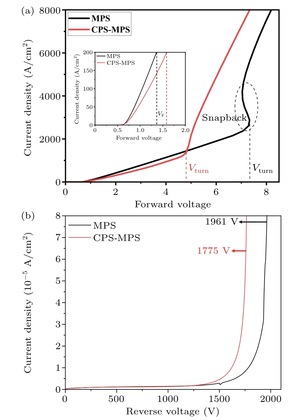
Fig.4.(a) Simulated forward I–V characteristics of a MPS diode and the CPS-MPS diode.The forward I–V characteristics in the low current regime are shown in the inset.(b)Simulated reverse I–V characteristics of a MPS diode and the CPS-MPS diode.
Figure 5 shows the 3D current distribution of the device after bipolar conduction.It can be seen from Fig.5(a) that when the device is turned on in the bipolar operating mode,the bipolar current of a MPS diode can only spread in the vertical direction, and the current is concentrated (13 kA·cm-2)under the P+ region.However, since the P+ regions of the CPS-MPS diode are connected to each other,the bipolar current of the CPS-MPS diode can spread in both vertical and horizontal directions,which lessens the current accumulation.The current density in the P+region is reduced to 8 kA·cm-2.Therefore, during the surge process, the energy of the CPSMPS diode can be dissipated more uniformly,[24]thereby reducing the temperature of the device surface and improving device reliability.

Fig.5.The 3D current distribution of the device after bipolar conduction:(a)MPS diode and(b)CPS-MPS diode.
Figure 4(b)shows the simulation results for the reverseI–Vcharacteristics of a traditional MPS diode and the CPS-MPS diode.The breakdown voltages of the traditional MPS diode and the CPS-MPS diode are 1962 V and 1775 V,respectively.In order to make the voltage drop of the CPS-MPS diode and the conventional MPS diode similar at the rated current,we set the thickness of the epitaxial layer of the CPS-MPS diode to be 2 μm smaller than that of the conventional MPS diode.These results then show that the breakdown voltage of the CPS-MPS diode is slightly smaller than that of the traditional MPS diode.
3.2.Surge current characteristics
The simulation circuit of the device surge is shown in Fig.3.During the simulation process,a half-sine pulsed current signal with a pulse width of 10 ms is directly applied to the anode of the device.The peak current amplitude starts from 10 A·mm-2, and increases each time until the device fails.Figures 6 and 7 show the simulation results for the surge process for a traditional MPS diode and the CPS-MPS diode,respectively.

Fig.6.(a)The I–V trajectories of a MPS diode during the surge current simulation.(b)The internal temperature change of the MPS diode during the surge.

Fig.7.(a)The I–V trajectories of the CPS-MPS diode during the surge current simulation.(b)The internal temperature change of the CPS-MPS diode during the surge.
Figure 6(a) shows the simulatedI–Vcurves of a traditional MPS diode at different current densities,and figure 6(b)shows the internal temperature change of the MPS diode during the surge process.When the current density applied to the anode of the MPS diode is 69 A·mm-2,the MPS diode reaches its highest temperature (T=931 K) at a time oft=5.7 ms;this temperature exceeds the melting temperature of Al, resulting in device failure.Similarly,figures 7(a)and 7(b)show the simulatedI–Vcurves and internal temperature change,respectively, of the CPS-MPS diode at different current densities.The current density at which the CPS-MPS diode fails is 83 A·mm-2, and the voltage drop at this current density also reaches a maximum, which is 6.4 V.As can be seen from the figure, the on-state voltage drop of the CPS-MPS diode is lower than that of the MPS diode during the surge process,which means that the on-state resistance of the CPSMPS diode is relatively low.The low on-resistance generates a small quantity of heat when the current is flowing, so the CPS-MPS diode has a relatively low device junction temperature during the surge process.
From Figs.6(a) and 7(a) it can be observed that, unlike a traditional MPS diode,the occurrence of the snapback phenomenon during the surge process is suppressed in the CPSMPS diode.This is due to the fact that the P+regions of the CPS-MPS diode are connected to each other,and the conduction voltage of the P–N junction is lower.This enables the CPS-MPS diode to enter the bipolar mode earlier than a traditional MPS diode and reduces the voltage drop in the drift region, thereby suppressing the occurrence of the snapback phenomenon.
Figure 8(a)shows the variation in the maximum junction temperature of a conventional MPS diode and the CPS-MPS diode with the magnitude of the surge current during the surge process.It has been reported that device failure can occur when the lattice temperature of the device is greater than the melting point of Al(933 K),at which point the surge current is defined as the surge capacity.It can be seen from Fig.8(a)that the surge capacity of the traditional MPS diode is 69 A·mm-2while that of the CPS-MPS diode is 83 A·mm-2, an increase of 20.29%.Figure 8(b) shows the surge energy at different surge currents.The maximum surge energies of the traditional MPS diode and the CPS-MPS diode are 2.59 J and 2.98 J,respectively, an increase of 15.06%.This result shows that the proposed CPS-MPS diode has a stronger anti-surge capability than a traditional MPS diode.
The CPS of the CPS-MPS diode ensures the rapid diffusion of the bipolar conduction plasma over the entire P–N junction surface during the surge process.This enables the establishment of a uniform current distribution and a more uniform temperature distribution, which avoids the formation of hotspots and the premature thermal runaway of the device.As shown in Fig.5(b),in the surge process of the CPS-MPS diode,once the bipolar conduction is activated at only one point of the P–N junction, the conductive plasma diffuses rapidly across the entire P–N junction, thereby providing a uniform bipolar current that can prevent heat accumulation.Since the CPS-MPS diode has a larger P+ area than a traditional MPS diode, during bipolar conduction the CPS-MPS diode injects more holes into the drift region,resulting in a stronger conductance modulation effect and leading to a lower resistance of the drift region.Therefore, under the same surge current impact,the junction temperature of the CPS-MPS diode is considerably lower than that of a traditional MPS diode.
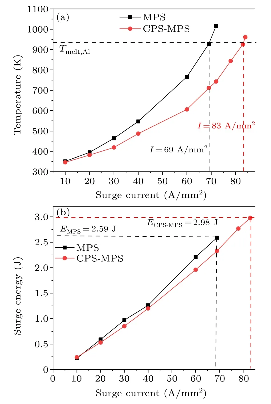
Fig.8.Summary of (a) temperature and (b) surge energy at different surge currents for a MPS diode and a CPS-MPS diode.
3.3.Analysis of the surge process
From Figs.6(a) and 7(a), it can be seen that during the surge process the voltage hysteresis appears in theI–Vcurves of the devices’current rise and fall.Furthermore,as the surge current increases, the hysteresis becomes more pronounced.As can be seen in Fig.9, the device junction temperature increases with the applied surge current;furthermore,the curves exhibit a clear hysteresis.Specifically, the device junction temperature obtained with decreasing current is always higher than that obtained with increasing current.The reason for this phenomenon is that when the temperature increases, the mobility decreases rapidly, leading to an increase in the onresistance of the device,which in turn generates a larger quantity of Joule heat and a higher junction temperature.Therefore,the on-resistance of the device upon decreasing the surge current is greater than the on-resistance upon increasing the surge current, resulting in a greater voltage with decreasing surge current,which in turn gives rise to a hysteresis phenomenon.

Fig.9.Curve of current density and temperature during surge.

Fig.10.The I–V trajectories of the CPS-MPS diode when the surge current is 83 A·mm-2.The internal temperature change of the CPS-MPS diode is shown as the inset.
Figure 10 shows theI–Vcurve and temperature change of the CPS-MPS diode when the surge current is 83 A·mm-2.The whole surge process is divided into five stages for the analysis.In stage I,the device behaves like a Schottky diode,working in unipolar mode, and the temperature is always increasing.The carrier mobility decreases as the temperature increases,so the on-resistance of the device gradually increases and the forward voltage drop continues to increase.[25]In stage II, the CPS-MPS diode enters the bipolar working mode and a large number of holes in the P+region are injected into the drift region, resulting in a conductance modulation effect, so the on-state voltage drop of the device is rapidly reduced.Figures 11(a)and 11(b)show the 3D current density distribution of the CPS-MPS diode at pointscandaindicated in Fig.10,respectively.It can be seen that after the conductance modulation, the current is uniformly distributed in the P+ region,and the P+ region conducts a large current.In addition, it is proved again that during the surge process of the CPS-MPS diode, as long as the P–N junction is turned on, the current spreads to the entire P+region,preventing current accumulation.From Fig.11(b), it can be concluded that at a low current the P–N junction of the CPS-MPS diode is not turned on,the conductance modulation effect does not occur and the current flows predominantly through the Schottky contact.Figure 11(c)shows the distribution of the internal hole concentration of the CPS-MPS diode at pointc.From this figure,it can be clearly seen that the hole concentration in the drift region after conductance modulation is significantly higher than that before conductance modulation(Fig.11(d)).
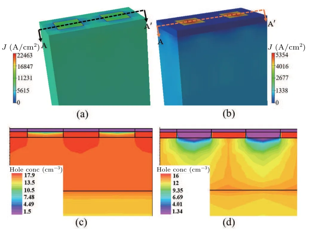
Fig.11.(a) The current distribution of the CPS-MPS diode at point c in Fig.10.(b) The current distribution of the CPS-MPS diode at point a in Fig.10.The hole concentration distribution of cross section A–A′:(c)after conductance modulation and(d)before conductance modulation.
In stage III,the surge current reaches its maximum value and then begins to decrease.The surge current reaches its maximum value at 5 ms, but the temperature is at its highest at 5.4 ms, and the temperature exhibits a lag.This lag is caused by the fact that the heat dissipated by the device is less than it generates.Additionally, at this stage, the holes in the P+ region have been completely injected into the drift region and the minority carrier concentration in the drift region reaches a maximum; the on-state voltage drop increases rapidly as the current increases.In stage IV,the surge current begins to decrease, and the conductance modulation effect in the drift region becomes less pronounced.At pointe,the device changes from the bipolar to the unipolar operation mode.In stage V,the CPS-MPS diode works in unipolar mode again.Since the temperature of the device when the surge current decreases is higher than that when the surge current increases,the carrier mobility decreases and the on-resistance increases with decreasing surge current,resulting in voltage hysteresis.
3.4.Turn-off characteristics
Figure 12 shows the reverse recovery characteristic curves of a conventional MPS diode and the CPS-MPS diode.The reverse recovery current of the CPS-MPS diode is larger than that of the traditional MPS diode.This is because the P+area of the CPS-MPS diode is larger and more minority carriers need to be extracted during reverse recovery.However,the reverse recovery time of the two diodes is almost the same;thus,CPS-MPS diodes are also suitable for high-frequency operating conditions.

Fig.12.Reverse recovery characteristics of a MPS diode and a CPS-MPS diode.
4.Conclusion
This work proposes a novel anode layout to improve the surge capability of traditional MPS diodes and investigates the entire surge process of the proposed device.Unlike the traditional structure, the structure proposed in this study has a CPS,which makes the current and temperature distributions of the device more uniform during the surge process and avoids the premature failure of the device caused by heat accumulation.Furthermore, the proposed layout structure suppresses the occurrence of the snapback phenomenon when the device switches from unipolar to bipolar operation.Through Silvaco TCAD simulations, the surge capacity of the structure proposed in this work was found to increase by 20.29%compared with that of a traditional MPS diode,and the surge energy increased by 15.06%.In addition, the bipolar conduction voltage of the CPS-MPS diode was found to be 4.45 V, which is 64.72% lower than that of a traditional MPS diode; this enables the device to enter the bipolar mode earlier in the surge process and improves the reliability of the device.
Acknowledgments
Project supported by the National Research and Development Program for Major Research Instruments of China (Grant No.62027814), the National Natural Science Foundation of China (Grant No.61904045), and Zhejiang Provincial Natural Science Foundation of China (Grant No.LQ20F040004).
猜你喜欢
杂志排行

Chinese Physics B的其它文章
- Robustness of community networks against cascading failures with heterogeneous redistribution strategies
- Identifying multiple influential spreaders in complex networks based on spectral graph theory
- Self-similarity of complex networks under centrality-based node removal strategy
- Percolation transitions in edge-coupled interdependent networks with directed dependency links
- Important edge identification in complex networks based on local and global features
- Free running period affected by network structures of suprachiasmatic nucleus neurons exposed to constant light