A 4H-SiC trench MOSFET structure with wrap N-type pillar for low oxide field and enhanced switching performance
2022-08-01PeiShen沈培YingWang王颖andFeiCao曹菲
Pei Shen(沈培), Ying Wang(王颖), and Fei Cao(曹菲)
1The Key Laboratory of RF Circuits and Systems,Ministry of Education,Hangzhou Dianzi University,Hangzhou 310018,China
2The School of Mechanical and Electronic Engineering,Pingxiang University,Pingxiang 337055,China
Keywords: 4H-silicon carbide (4H-SiC) trench gate MOSFET, breakdown voltage (VBR), specific onresistance(Ron,sp),switching energy loss,super-junction
1. Introduction
Wide-band gap third-generation semiconductor material silicon carbide offers excellent switching properties, temperature stability and low electromagnetic interference (EMI),making it ideal for next-generation power conversion applications such as switching power supplies, electric vehicles,and industrial power.[1–4]In recent years, SiC power MOSFETs with theVBRof 600–1700 V level dominated have been commercialized,but higherVBRof the SiC MOSFETs are less studied. Especially, the SiC trench gate MOSFET generally has lowRon,spdue to the small cell-pitch using the trench gate configuration.[5–7]However, SiC trench gate MOSFET has a fatal disadvantage. As the drain–source voltage increases,the electric field at the bottom corner of the gate trench increases,affecting the gate oxide stability.[8,9]To overcome this issue,some good methods and novel structures are proposed to overcome the electric field concentration at the bottom corner of the gate trench.[10–12]The most commonly used way to shield highly the electric field at the bottom corner of the gate trench is to increase the p+shield region under the gate trench,[13–15]yet with a marked increase inRon,sp. With charge-balanced npillar and p-pillar,the super-junction(SJ)MOSFET has more superior electrical characteristics compared with conventional SiC trench MOSFET.[16–20]Vudumulaet al.[16]studied the static and dynamic characteristics of the CoolSiC trench MOSFET structure by introducing the concept of super-junction,and the structure provides a good trade-off between gate oxide reliability andRon,sp. Oroujiet al.[17]proposed to replace the p+shield region with an n-type pillar and a p-type pillar at the bottom of the gate trench. The new device structure improves theVBRand reduces theRon,sp,and has good switching characteristics. Denget al.[18]studied a novel structure embedded in a floating p-column in the drift region,which ensures that theVBRis not reduced, allowing for a compromise between theRon,sp, and the short-circuit characteristics. Kim[19]proposed a novel SJ structure with a hetero-junction diode for improved reverse recovery characteristics and switching energy loss. Heet al.[20]investigated a new SJ structure by using grounded p+buried layers and connected p columns to encapsulate deep trench gate oxide to reduce the saturation current.
Moreover, the practical feasibility of fabricating superjunction structures has been discussed by using the trenchfilling epitaxial growth method in some papers. Jiet al.[21,22]studied and made possible uniform epitaxial filling in the 4HSiC trench between 7 μm and 50 μm deep. There have also been significant advances in understanding the mechanisms of epitaxial growth of trench filling.[23–25]In addition, Ryojiet al.[26]have established a key manufacturing process of superjunction structure with thickness over 20 μm and high aspect ratio, and the theoretical limit of 6.5-kV class 4H-SiC superjunction MOSFET is broken through by the trench filling epitaxial growth method. Consequently,it is feasible to study the trench-filled epitaxial growth method of SiC super-junction devices with high breakdown voltage.
In this article, an improved structure of 4H-SiC trench gate MOSFET with a side-wall p-pillar and a wrapping npillar at the right of the p-pillar is studied to reduce the gate oxide electric field and switching energy loss. The Silvaco TCAD simulation results demonstrate that the SNPPT-MOS exhibits good static and dynamic performance. The SNNPTMOS structure is a significant optimization of the full-SJ-MOS structure. In addition,in the second section,some preliminary manufacturing techniques are discussed, and their feasibility is proved from the processing point of view.
2. Description of the device structure and fabrication procedure
Figure 1 shows the schematic cross-section of the SNPPTMOS and full-SJ-MOS.[27]The main device-related parameters of the two structures are shown in Figs.1(a)and 1(b). The SNPPT-MOS structure mainly includes a p+-SiC buried region,CSL region,a p-pillar,and a wrap n-pillar. The gate oxide thickness of both sidewalls and the bottom is about 50 nm.The height of the CSL region was 1.7 μm (LCSL=1.7 μm).The height of the p-pillar was 24 μm(Lp-pillar=24 μm). The wrapped n-pillar junction depth (Lwn) was set to be 1 μm to decrease the impact toVBRand gate-drain charge. The distance between the wrap n-pillar and the gate was set at 0.5 μm(Wng= 0.5 μm). The thickness of the gate oxide was set at 50 nm. The n-drift region dopant concentration (Nd) was set to be 3×1015cm-3. Moreover, in the super-junction (SJ)MOSFET structure, the charge balance between the n-pillar and p-pillar must be precisely controlled. Thus, the products of the width and doping concentration of the n-pillar region of the two structures must equal to the product of the width and doping concentration of the p-pillar region the according to[16,17,28,29]
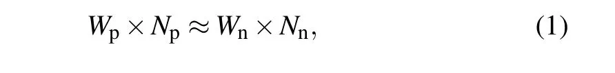
whereWpandWnare the widths of the p-pillar and n-pillar,NpandNnare doping concentrations of the p-pillar and n-pillar,respectively. The detailed parameters of the simulation used for the two structures are listed in Table 1.
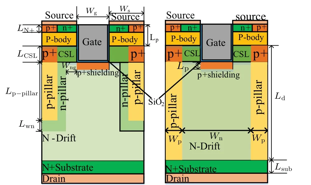
Fig. 1. The schematic cross-section of the (a) SNPPT-MOS and (b)full-SJ-MOS.
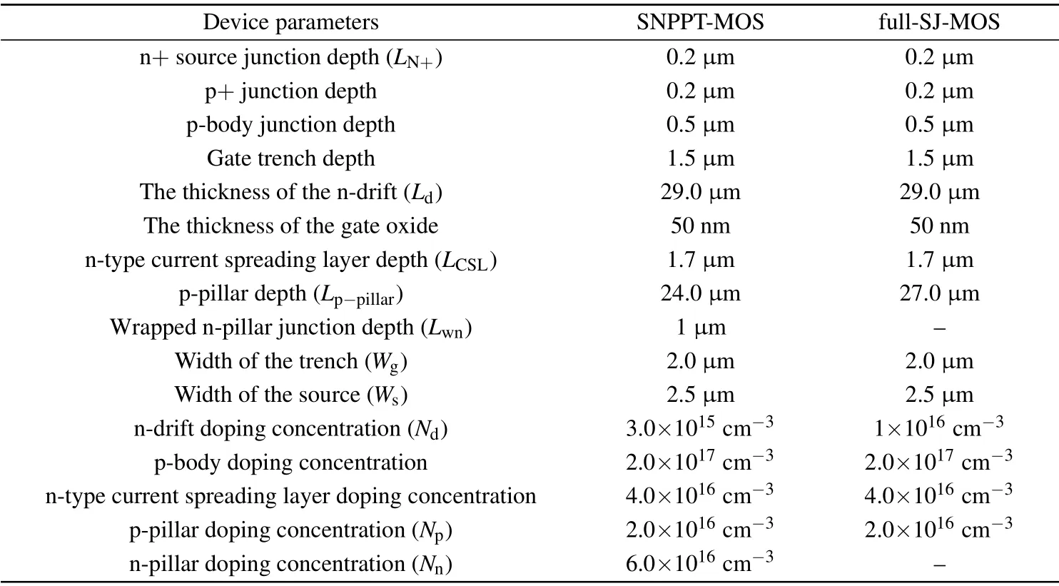
Table 1. Device parameters in simulations.
A feasible manufacturing process of the SNPPT-MOS is shown in Fig. 2. An n-drift was grown on a 4H-SiC n+substrate, as shown in Fig. 2(a). Fabrication of the superjunction structure began with a deep stripe-trench formation in an n-drift by using inductively coupled plasma etching in an SF6/O2gas ambient, as shown in Fig. 2(b). The p-pillar region was fabricated with the trench-filling epitaxial (TFE)growth method,[26]as shown in Fig.2(c). After TFE growth,the wafer surface was flattened by thinning the TFE grown wafer to the initial epitaxial wafer thickness by using grinding and polishing,as shown in Fig.2(d). And then,CSL grew on the flat surface of the wafer. After CSL was formed, a mask plate of a certain size(distance between the two p-pillar)was manufactured to mask CSL, and p+-SiC buried region were generated on both sides of the mask plate through ion implantation. The resulting structure is shown in Fig. 2(e). Then remove the mask based on the structure in Fig.2(e),and grow another layer of p-type 4H-SiC to form the p-body region. After the p-body region was formed, n+-SiC source region was formed by ion implantation. Then, masks of the same size were used to mask certain n+-SiC source region,and p+-SiC source region was generated on both sides of the mask by ion implantation. The final structure is shown in Fig.2(f). Finally,the p+-shielding, the oxide layer, the gate structure, and the electrode were implemented in a similar way to the conventional SiC trench MOSFET,as shown in Figs.2(g)and 2(h).
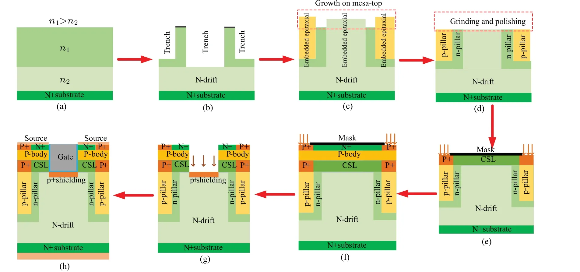
Fig.2. The key fabrication procedure of the SNPPT-MOS.
Moreover, it is a very important step to align p+-SiC buried region and p+-SiC source region with p-pillar in the process of SNPPT-MOS structure.Firstly,for Fig.1(d),ensure that the polishing process thinned the epitaxial wafer to the initial thickness of the epitaxial wafer, so that the wafer surface becomes sufficiently flat. Secondly, the size of the mask in Fig.1(e)can be determined, that is, the distance between the p-pillar on both sides. In addition, in SiC devices, due to the low diffusion coefficient of dopant,[30]p+-SiC buried region is formed by ion implantation,and the doping amount of ion implantation impurity can be precisely controlled. For Fig.1(f),the p+-SiC source region is firstly formed by ion implantation on both sides of the n+-SiC source region. The mask used is the same size as that used in Fig.1(e). And the p+-SiC source region on both sides of the n+-SiC source region is also formed by ion implantation,which can accurately control the amount of impurity doping. Therefore,the accurate alignment of align p+-SiC buried region and p+-SiC source with p-pillar is ensured to a certain extent.
At the same time, in order to better illustrate the feasibility of SNPPT-MOS structure. TheVBR,Ron,sp, and FoM(V2BRRon,sp)of p+-SiC buried region width and p+-SiC source region width from-10% to +10% deviation are simulated and discussed, as shown in Table 2. As can be seen from Table 2, theVBRandRon,spof the device are almost constant when the error of the alignment widths of the p+-SiC source region and p+-SiC buried region with p-pillar ranges from 0 to-10%. When p+-SiC source region and p+-SiC buried region are aligned with the width of p-pillar from 0 to+10%,theVBRof the device increases slightly and then decreases slightly,theRon,spchanges accordingly,and the FoM(V2BRRon,sp)is calculated to be almost the same.
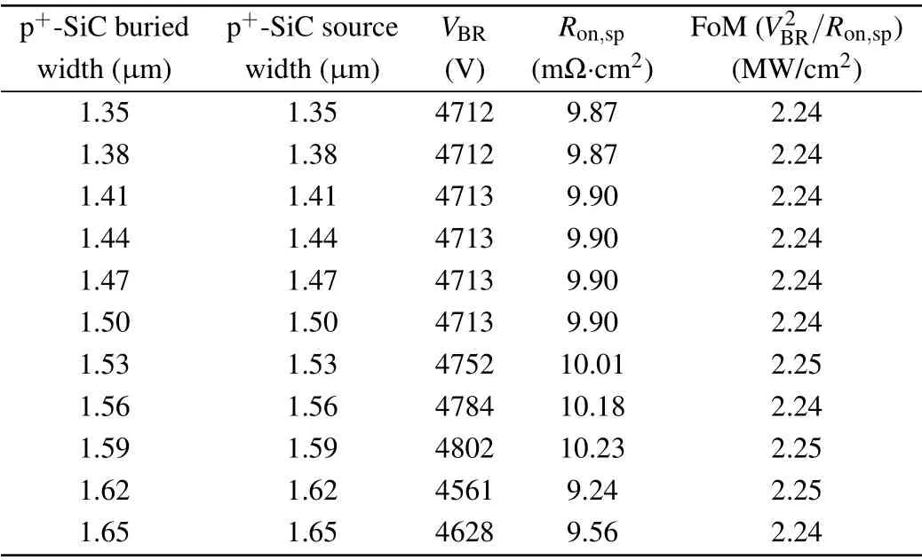
Table 2.The VBR,Ron,sp and FoM(V2BR/Ron,sp)of p+-SiC buried region width and p+-SiC source region width from-10%to+10%.
3. Numerical simulation and result analysis
In this section,the static characteristics and the dynamic characteristics of the SNPPT-MOS were simulated by using the 2-D Silvaco ATLAS tool and compared the performance of the full-SJ-MOS with the performance of the SNPPT-MOS.In this simulation, some physical models were used. The physical models are divided into four parts. The first part is the mobility model, where the simulation uses the concentration and temperature-related mobility model(ANALYTIC)and the parallel electric field correlation model(FLDMOB).The second part is the composite model, where the simulation uses the Shockley–Read–Hall complex model(SRH)and the Auger complex model(AUGER).The third part is the carrier generation model, where the IMPACT SELB model is used in the simulation. The fourth part is the carrier statistical model.The incomplete ionization model (INCOMPLETE) is used in the simulation.[31–33]
3.1. On-state characteristic
The on-state output characteristic curves of the SNPPTMOS and full-SJ-MOS atVgs=20 V,Vgs=16 V,Vgs=12 V,andVgs=8 V are shown in Fig.3. TheRon,spof the SNPPTMOS was 9.90 mΩ·cm2, and theRon,spof the full-SJ-MOS was 11.5 mΩ·cm2,atVgs=16 V andVds=1 V.The wrap npillar and CSL region in the optimized structure provide two diffusion paths for current diffusion and compress the depletion region. The thin light doping of the CSL region causes the electrons to diffuse horizontally earlier.
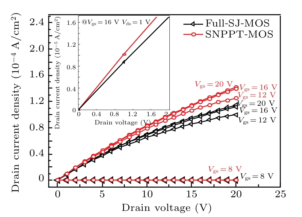
Fig. 3. The on-state output characteristic curves for the SNPPT-MOS and full-SJ-MOS.
In addition, the wrap n-pillar allows the current to flow vertically. We know that the more narrow the depletion region, the wider the current path of the electron, resulting in the lowestRon,sp. Compared with full-SJ-MOS, theRon,spof SNPPT-MOS decreased by 16.2%. TheRon,spof the SNPPTMOS is slightly lower than that of full-SJ-MOS because the SNPPT-MOS structure has a higher doping concentration in wrap n-pillar. In the SNPPT-MOS structure,the wrap n-pillar under the CSL the electron concentration in the channel region,while the depletion region decreases,increasing the current path in the SNPPT-MOS structure, as shown in Fig. 4.The equation of theRon,spcan be described as
whereWdis the maximum depletion width and theμnis the electron’s mobility.

Fig.4. Distribution of the electron concentration for (a) SNPPT-MOS and(b)full-SJ-MOS.
3.2. Off-state characteristics
Figure 5 shows the off-state breakdown characteristic curves for the SNPPT-MOS and full-SJ-MOS. The corresponding electric field in the gate oxide distributions is shown in Fig.6.
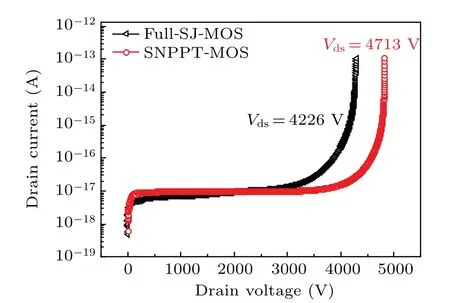
Fig.5. OFF-state breakdown characteristic curves of the SNPPT-MOS and full-SJ-MOS.
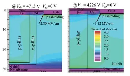
Fig. 6. OFF-state corresponds to electric field curves of (a) SNPPTMOS and(b)full-SJ-MOS.
We can see that the peak electric field in the gate oxide (Epeak-goe) in the full-SJ-MOS structure has reached 3.12 MV/cm with a drain bias voltage of 4226 V. In the SNPPT-MOS structure, the value of theEpeak-goeis about 2.80 MV/cm with a drain bias of 4713 V. The SNPPT-MOS exhibits lowerEpeak-goethan the full-SJ-MOS,this is because of the mutual depletion effect of the p-pillar and the wrap npillar in the n-drift,and the electric field around the bottom of the gate trench could be screened effectively. As for the full-SJ-MOS structure,it could also alleviate the high electric field around the bottom of the gate trench to a certain extent due to the p-pillar embedded n-drift region, while the high doping concentration of the n-drain region and thus theEpeak-goe(3.12 MV/cm)is slightly higher than the SNPPT-MOS,resulting in aVBRwitha drain bias of 4226 V. The vertical electric field distributions of the SNPPT-MOS and the full-SJ-MOS from 0 to 30 μm are shown in Fig. 7. The maximum gate oxide electric field is about 2.5 μm vertically. From 2.5 μm onward,the vertical electric field curve of SNPPT-MOS is almost as flat as that of the full-SJ-MOS.Because of the mutual depletion effect of the p-pillar and the wrap n-pillar in the ndrain region,the field distributions for the SNPPT-MOS at the p-pillar and the wrap n-pillar interface are uniforms.
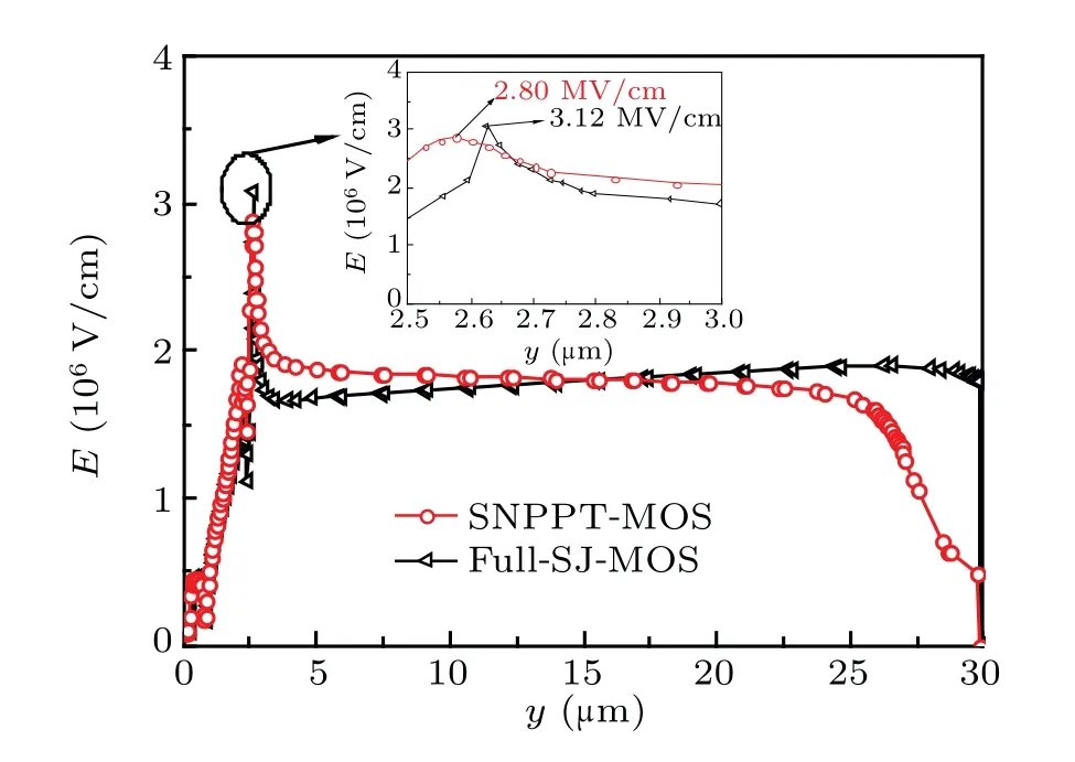
Fig.7. The vertical distribution of the electric field from 0 to 30 μm.
3.3. Reverse transfer capacitance and gate charge characteristics
The smaller reverse transfer capacitance is of great importance for reducing the switching loss and preventing the false turn-on. It helps improve the switching characteristics.The reverse transfer capacitance(Crss=Cgd)properties of the SNPPT-MOS and full-SJ-MOS are shown in Fig.8.Compared with theCrssof the full-SJ-MOS,the SNPPT-MOS exhibits a lowerCgdthan the full-SJ-MOS,owing to the effective electric field shielding of the p-pillar and wrap n-pillar. And they have a smaller p–n junction area than the conventional full superjunction structure.
The specific gate charge (Qg,sp) characteristic curves of the SNPPT-MOS and the full-SJ-MOS are evaluated as well,as shown in Fig. 9. TheQg,spis extracted by using the mixmode simulation. The simulation circuit schematic diagram is inserted in the bottom right corner of Fig. 9. The extractedQgd,spof the SNPPT-MOS is 101 nC/cm2.The SNPPTMOS exhibits a lower miller charge compared with that of the 154 nC/cm2for the full-SJ-MOS due to the p-pillar and wrapped n-pillar having smaller p–n junction area and effective electric field shielding ability. The FoM (Ron,sp×Qgd,sp)is a widely used parameter to measure the device performance in high-frequency switching applications.[34–36]According to the calculation, the FoM (Ron,sp×Qgd,sp) of the full-SJ-MOS structure is 1771 mΩ·nC.The SNPPT-MOS structure obtained superiorRon,sp×Qgd,spwith a value of 999.9 mΩ·nC, which decreases by 77.1%compared with the full-SJ-MOS structure.
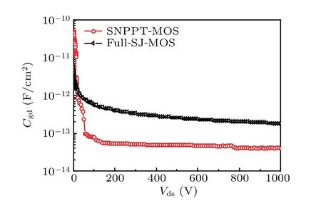
Fig.8. The Crss property curves of the SNPPT-MOS and full-SJ-MOS.
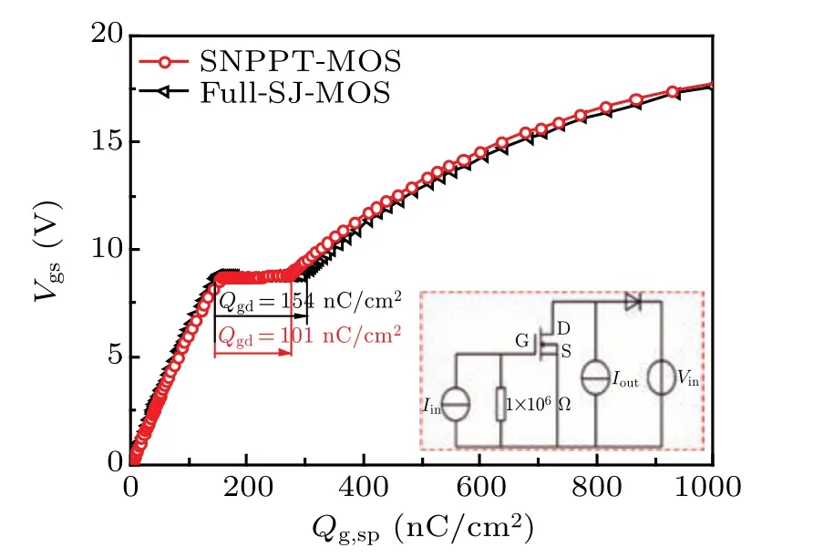
Fig.9. The Qg,sp characteristic curves of the SNPPT-MOS and full-SJMOS.
3.4. Dynamic characteristics
To better study the switching characteristics of the SNPPT-MOS, the double-pulse test (DUT) circuit is used to investigate the switching performance of the two structures,as shown in Fig. 10. The basic parameters of the DUT circuit are listed in Table 3. Figure 11 shows the switching waveforms of the SNPPT-MOS and full-SJ-MOS. As can be seen from Fig.11,the full-SJ-MOS needs a longer period to arrive at highVdsand highIdscompared with the SNPPT-MOS.TOFFis defined as the turn-off delay time and turn-off fall time.TONis defined as the turn-on delay time and turn-on fall time.
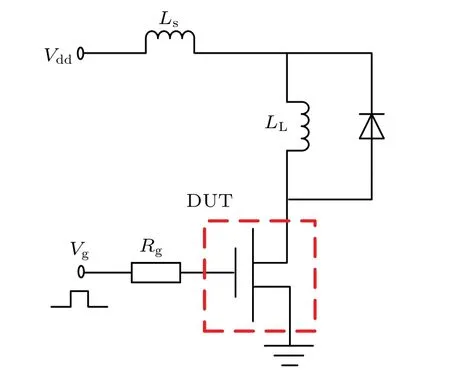
Fig.10. The double-pulse test circuit.
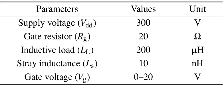
Table 3. The basic parameters of the DUT circuit.
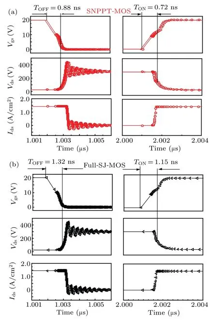
Fig.11. Switching waveforms of(a)SNPPT-MOS and(b)full-SJ-MOS.
Figure 12 shows the switching energy loss for the SNPPTMOS and the full-SJ-MOS. The calculated energy loss values of turn-on (Eon) and turn-off (Eoff) for SNPPT-MOS are 32.5 mJ/cm2and 31.7 mJ/cm2. The calculated values ofEonandEofffor full-SJ-MOS are 40.3 mJ/cm2and 36.5 mJ/cm2.It can be discerned that in the SNPPT-MOS structure,the energy loss duringEonis reduced as a respective decrease of 24.%compared with the full-SJ-MOS, and theEoffis a respective decrease of 15.1%compared with the full-SJ-MOS.The equation of theEonandEoffcan be described as
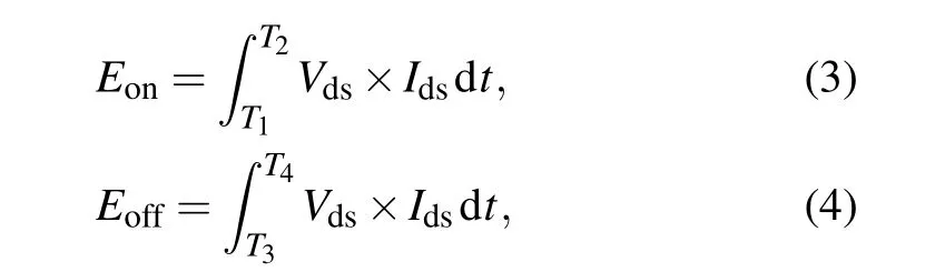
whereT1(10%ofVgs(on)),T2(2%ofVdd),T3(90%ofVgs(on))andT4(2%ofIds).
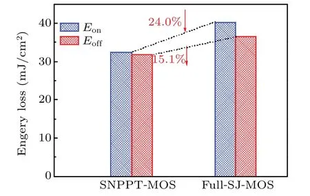
Fig.12. Switching energy loss of the SNPPT-MOS and full-SJ-MOS.
3.5. Parameters optimization
To get the optimized device structure,the added wrap npillar dopant concentration(Nn),p-pillar dopant concentration(Np),and the height of the p-pillar(H)have a great influence on the device performance. In the SJ MOSFET structure, to obtain highVBR,it is necessary to control accurately the charge balance between n-pillar and p-pillar regions. So the products of the width and concentration of the n-pillar region of the SNPPT-MOS must equal the product of the width and concentration of the p-pillar region. Figure 13 shows theVBRandRon,spof this SNPPT-MOS structure in the case ofNpfrom 1×1016cm-3to 3×1016cm-3,Nnfrom 3×1016cm-3to 9×1016cm-3, andHfrom 10 μm to 24 μm. And the FoM(V2BR/Ron,sp) corresponding to differentHis given in detail.Figure 14 shows FoM(V2BR/Ron,sp)as a function of the differentNn,Np,andH. The maximum FoM that appears at theNn,Np, andHare 6×1016cm-3, 2×1016cm-3, and 24 μm, respectively. We also investigated the most suitableWng. TheWngfrom 0.1 μm to 0.7 μm, as shown in Fig. 15, we can see that the smaller theWngwas, the smaller theRon,spof the SNPPT-MOS was. However, theVBRalso decreased. As can be seen from Fig. 15, we can find that the most suitableWngwas 0.5 μm.
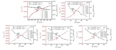
Fig.13. The VBR and Ron,sp as function Np and Nn for different heights of the p-pillar.
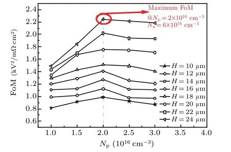
Fig.14. FoM(V2BR/Ron,sp)as a function of the different Nn,Np,and H.
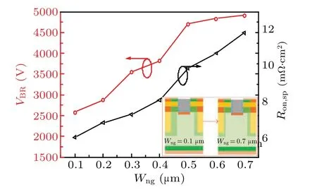
Fig. 15. The VBR and Ron,sp for the different distances between the npillar and the gate(Wng).
Table 4 gives theVBR,Ron,sp,and FoM whenWngis set at 0.5 μm. The higher theNn,and the smaller theVBRandRon,spof the SNPPT-MOS.The FoM value increases firstly and then decreases. The main reason is that whenNnis low,the depletion region in the n-pillar is wider, which makes the current path narrow. As theNnvalue increases, the electron path becomes wider. As the doping concentration of n-pillar is higher than that of drift,the increase ofNnsignificantly improves the reduction ofRon,sp. WhenNnis low, the reduction ofRon,sphas more effect on FoM than that ofVBR. However,whenNnis high,the effect of the decrease ofRon,spon FoM is less than that of the decrease ofVBR.
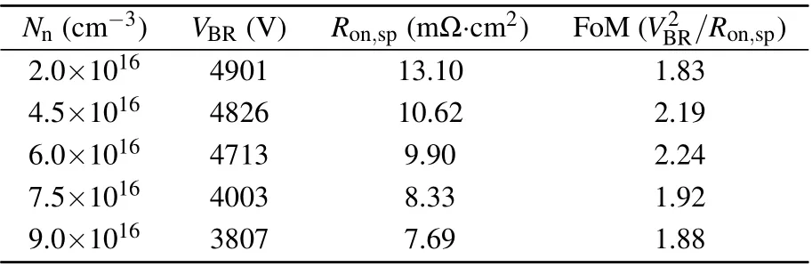
Table 4. The VBR,Ron,sp,and FoM at Wng=0.5 μm.
Table 5 gives theVBR,Ron,sp, and FoM whenNnis 6×1016cm-3. As can be seen from Table 5, we can find that the wider theWng, the larger theRon,spand theVBR. The FoM value increases firstly and then decreases. The main reason is that when theWngis smaller, the larger the area of the electron flow through the n-pillar. The area of electrons flow through in the n-pillar is larger than the depletion region. With the increase ofWng, the area of electrons flowing through the n-pillar increases. It is because of the high doping concentration of the n-pillar that the area of electrons flows through the n-pillar increases, which promotes the decrease ofRon,sp.WhenWngis small,the effect ofRon,spon FoM is greater than that ofVBR.With the increase ofWng,the contribution ofRon,spto FoM decreased. In the largerWngcondition,the increase ofRon,sphad less effect on FoM than that ofVBR. Therefore,we choose these two parameters as the basement of our simulations and the following discussion. The electrical property of the full-SJ-MOS and the SNPPT-MOS are listed in Table 6.
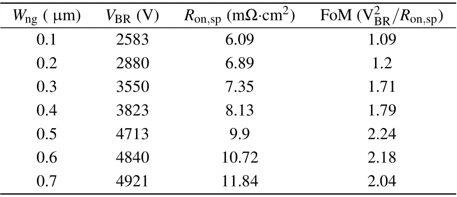
Table 5. The VBR,Ron,sp,and FoM at Nn=6×1016 cm-3.

Table 6. Electrical property of the SNPPT-MOS and the full-SJ-MOS.
4. Conclusion and perspectives
An optimized structure of the 4H-SiC trench MOSFET is studied in this article. The improved structure exhibits good electrical characteristics due to the incorporating side-wall ppillar region and a wrapping n-pillar region in the drift region.The SNPPT-MOS structure has significantly protected the gate oxide and relieves the electric field around the p+ shielding region. With charge-balanced n-pillar and p-pillar under the p-body,the improved structure help reducing theRon,sp,which leads to the tradeoff of theVBRandRon,sp. In addition, the improved structure exhibit superior switching property during both the turn-on and the turn-off transients.
Acknowledgements
This work was supported in part by the National Natural Science Foundation of China (Grant Nos. 61774052 and 61904045), the National Natural Science Foundation of Jiangxi Province of China (Grant No. 20202BABL201021),and the Education Department of Jiangxi Province of China for Youth Foundation(Grant No.GJJ191154).
猜你喜欢
杂志排行

Chinese Physics B的其它文章
- Solutions of novel soliton molecules and their interactions of(2+1)-dimensional potential Boiti–Leon–Manna–Pempinelli equation
- Charge density wave states in phase-engineered monolayer VTe2
- High-pressure study of topological semimetals XCd2Sb2(X =Eu and Yb)
- Direct visualization of structural defects in 2D semiconductors
- Switchable down-,up-and dual-chirped microwave waveform generation with improved time–bandwidth product based on polarization modulation and phase encoding
- Machine learning potential aided structure search for low-lying candidates of Au clusters