High-Efficiency Rectifier for Wireless Energy Harvesting Based on Double Branch Structure
2023-09-22CUIHengrong崔恒荣JIAOJinhua焦劲华YANGWeiJINGYuxiang荆玉香
CUI Hengrong(崔恒荣), JIAO Jinhua(焦劲华), YANG Wei(杨 威), JING Yuxiang(荆玉香)
College of Information Science and Technology, Donghua University, Shanghai 201620, China
Abstract:A rectifier circuit for wireless energy harvesting (WEH) with a wide input power range is proposed in this paper. We build up accurate models of the diodes to improve the accuracy of the design of the rectifier. Due to the nonlinear characteristics of the diodes, a new band-stop structure is introduced to reduce the imaginary part impedance and suppress harmonics. A novel structure with double branches and an optimized λ/4 microstrip line is proposed to realize the power division ratio adjustment by the input power automatically. The proposed two branches can satisfy the two cases with input power of -20 dBm to 0 dBm and 0 dBm to 15 dBm, respectively. Here, dBm = 10 log(P mW), and P represents power. An impedance compression network (ICN) is correspondingly designed to maintain the input impedance stability over the wide input power range. A rectifier that works at 2.45 GHz is implemented. The measured results show that the highest efficiency can reach 51.5% at the output power of 0 dBm and higher than 40% at the input power of -5 dBm to 12 dBm.
Key words:diode modeling; rectifier circuit; impedance compression network; power division strategy
Introduction
As an attractive energy supply method for micro-power Internet of things modules, wireless energy harvesting collects wireless energy signals in the environment and can realize a long-term maintenance-free energy supply[1-3]. The level of wireless energy harvesting mainly depends on the power conversion efficiency (PCE) of the radio-frequency to direct current (RF-DC) rectifier. However, in practical application scenarios, the RF energy density could vary substantially in different locations and environments[4]. Therefore, the input microwave power is typically dynamic for a rectifier[5]. For example, when powering an unmanned aerial vehicle (UAV), the RF energy received by the UAV varies with location[6]. The nonlinear characteristic of the diode[7-8]makes the input impedance of the diodes in a rectifier vary with the input power, resulting in an impedance mismatch and a severe drop in PCE[9].
In recent years, several attempts have been made to improve the performance of their rectifiers over wide input power ranges[10-12]. A resistance compression network (RCN)[13-15]was introduced to create a resistance-compressed rectifying circuit over 10 dB power range, but failed to compensate for the change in the input impedance based on the change of the input power; a rectifier with a self-tuning impedance matching (STIM) was designed to cope with the fluctuation of input power[16], which achieved 10% improvement of PCE at a low input power; a nonlinear power division strategy was applied to the input power level without any power dividers or couplers[17], showing an input power range exceeding 50% over 23 dB (6.5 - 29.5 dBm). All these solutions mainly focused on the input power range over 0 dBm, which led to the low conversion efficiency of micro-power, since the RF energy in the living environment is often below 0 dBm.
Therefore, an efficient rectifier circuit structure based on the nonlinear impedance characteristics of diodes is proposed, which is applicable to medium and low input power (from -5 dBm to 12 dBm). A new band-stop structure[18]was introduced to realize harmonic suppression and impedance tuning of the imaginary part of the diodes; the power division strategy was implemented by optimizing theλ/4 microstrip line, so that the low input power rectifier operated from -20 dBm to 0 dBm and the high input power rectifier could operate from 0 dBm to 15 dBm. A novel impedance compression network was adopted to broaden the input power range of the rectifier, and further to obtain impedance matching over a wider input power range (over 20 dB). For validation, 2.45 GHz rectifier was implemented. The rectification efficiency was higher than 40% at the input power of -5 dBm to 12 dBm, and the maximum conversion efficiency reached 51.5% at the output power of 0 dBm.
1 Basic Principle of Rectifier Circuit
The rectifier consists of a matching network, two rectifier diodes, a direct current (DC) pass filter, and two impedance loads. And the basic schematic diagram is shown in Fig.1. The receiving antenna transforms the microwave power in the free space into the high-frequency current in the local circuits, and the rectifier converts alternating current (AC) to DC using the unidirectional conductivity of the diode. The circuit topology consists mainly of half-wave, full-wave, bridge, and voltage doubling rectifiers. The rectifier circuit in this study is based on the half-wave rectifier structure of a single diode in parallel.

Fig.1 Basic schematic diagram of rectifier circuit
1.1 Analysis of diode principle
The analysis is based on the equivalent spice model, as shown in Fig. 2, whereRSdenotes series resistance introduced by the package, whileRjandCjrepresent junction resistance and junction capacitance of the diode, respectively. Due to the nonlinear characteristics of the diode, its junction resistance and junction capacitance fluctuate with frequency and input power, making it possible for the nonlinear characteristics of Schottky diodes to be adopted for designing the rectifier.VinandV0represent the input voltage and load voltage, respectively.RLis the load resistance. Based on the nonlinear model of the Schottky diode, the input impedance of the Schottky diode at a fixed load is
(1)
whereθONis the turn-on angle of the diode.

Fig.2 Equivalent spice model of Schottky diode
The diode capacitance can be balanced by series inductance, and then, the impedance of the diode can be tuned to an almost pure resistance.
(2)
The SMS7630 and the HSMS286B are different rectifier diodes. The SMS7630 is suitable for low power levels because of its low forward conduction voltage, while the HSMS286B is suitable for high power levels because of its high reverse breakdown voltage.
1.2 Accurate modeling of diodes under small-signal conditions
The above analysis of the diode fails to take into account the actual package parameters of the diode. The spice model of the diode used in the advanced design system (ADS) simulation is still subject to some errors compared with the actual diode model, which makes it necessary to model the diode accurately. And the model can be used to design the rectifier circuit to improve the rectification efficiency.
1.2.1Diodemodelingprinciples
The equivalent circuit model of the diode is shown in Fig. 3, whereLPandCPrepresent package inductance and capacitance of the diode, respectively, andLP,CP, andRSare voltage-independent parameters;CjandRjare voltage-dependent parameters. In order to extract the diode model parameters, voltage-independent component parameters should be first extracted. Then, the measured Scattering parameters (S-parameters) of the diode are imported into ADS to generate S2P components, where S2P file is Sonnet S-device Parameter Data File.LP,CPandRSnegative components are added at the periphery of the circuit, and an optimizer in ADS is used to optimize the negative component parameters. When the real part of the admittance parameters (Y-parameters) at different voltages is a straight line, the imaginary line can be diagonal. Finally, the expressions ofRjandCjcan be obtained by data fitting.
Ijis the junction current andVdis the junction voltage. The diode junction current equation is
Ij=I0eVd/(nVt)-1,
(3)
whereVtis the thermal voltage with a value of 25.69 mV at room temperature;I0is the saturation current;nis the ideality factor. Fitting a series of (Vd,Ij) values can yield the parametersI0andn.
The expression of diode junction capacitance is
(4)
The parametersFc,VjandC0can be obtained by fitting a series of (Vd,Cj) values, and the expression of diode junction capacitance can also be determined.

Fig.3 Diagram of parameter extraction of voltage-independent components
1.2.2Modulescene
The process of diode modeling mainly includes the following steps,i.e., calibrating the vector network analyzer, measuring S-parameters of the diode, and extracting equivalent circuit parameters of the diode.
We calibrated the vector network analyzer using the short-open-load-thru (SOLT) calibration method. The total length of the test fixture is 30 mm, leaving 3 mm diode welding position in the middle. A circle of metal vias around the microstrip line atλ/20 hole spacing is made to reduce the edge radiation of printed circuit board (PCB). The physical drawing of the test fixture and its corresponding straight-through fixture calibrator are shown in Fig. 4(a). Measurement of diode S-parameters requires a vector network analyzer, DC voltage regulator, bias tee, test fixture, and its straight-through fixture. The rectifier operates within the vector network analyzer measurement range of 0-10 GHz and the actual measurement circuit is shown in Fig. 4(b).

Fig.4 Test scenarios:(a) test fixture and straight-through fixture; (b) actual measurement diagram of diode
As shown in Fig.5,S11is the return loss andS21is the inset loss. The measured S-parameters of the HSM286B match the simulated S-parameters of the model in ADS, making it not necessarily important to model the HSM286B accurately. As shown in Fig. 5(b), the measured S-parameters of the SMS7630 differ significantly from those of the spice model, which requires the actual model of SMS7630 to be built based on the equivalent diode circuit.

Fig. 5 Comparison between measured S-parameters and simulated S-parameters:(a) HSMS286B and model provided by ADS; (b) SMS7630 and spice model based on datasheet
1.2.3Parametersobtainedbyfinalmodeling
ADS simulation optimization showsLPof 2.4 nH,CPof 0.11 pF, andRSof 20 Ω. Then, according to formulas (3) and (4), by using the least square method fitting theI-Vcurve andC-Vcurve can be yielded, respectively. The fitting curves are shown in Fig. 6(a), and the fitting parameters are shown in Table 1. The equivalent circuit model of diode SMS7630 is established as shown in Fig. 6(b), which is consistent with the established model.

Fig. 6 Results of diode modeling:(a) I-V and C-V curve fitting diagram; (b) comparison of measured S-parameters and simulated model S-parameters

Table 1 Diode actual model parameters
2 Design of Rectifier Circuit
2.1 New impedance compression network
The junction capacitance and junction resistance of the diode change with the voltage across the diode according to the above analysis on the Schottky diode. The input impedance of the rectifier can change accordingly with the change of the input power, making it difficult to keep matching the rectifier impedance with the receiving antenna impedance in a wide input power range and resulting in a lower efficiency of the rectifier. Therefore, a novel impedance compression network is introduced to reduce the sensitivity of the rectifier impedance to the change of input power, where a parallel open microstrip line and a parallel shorted microstrip line are added between the rectifier circuit and the receiver antenna. The two microstrip lines have the same characteristic impedance, the sum of the electrical length isλ/2, and the electrical lengths of the microstrip lines are not 0,λ/4 andλ/2. Figure 7(a) is a schematic diagram of the new impedance compression network structure.

Fig. 7 Impedance compression network:(a) schematic diagram of new impedance compression network structure; (b) comparison between Zinbefore and after compression
The input impedance of the rectifier is expressed as
ZL=RL+jXL.
(5)
The electric length of TL1 isθ1, the electrical length of TL1 isθ2, and
θ1+θ2=π.
(6)
The characteristic impedances of TL1 and TL2 are bothZ0, and then the total conduction of these two branches is expressed as
(7)
The input impedance can be derived as

(8)
Based on the above expression, the input impedance expression of the circuit contains real and imaginary parts after the impedance transformation. WhenZLis higher than or close toZ0, the denominator is much higher than 1; when the original valueZLis greatly compressed, and the range of input impedance variation is narrowed to achieve the purpose of impedance compression. From the structural perspective, the new impedance compression network adopted in this paper is simple and practical.PinandVoutrepresent input power and output voltages, respectively; real(Zin) and imag (Zin) represent real and imaginary parts ofZin, respectively.
The electrical lengths of TL1 and TL2 in this paper areλ/6 andλ/3, respectively, and their characteristic impedances are both 50 Ω. Before impedance compression, the real impedance of the rectifier fluctuates from 40 Ω to 70 Ω, while the imaginary impedance of the rectifier fluctuates from -90 Ω to 20 Ω. The comparison results after introducing the novel impedance compression network are shown in Fig. 7(b). After impedance compression, the real impedance fluctuates from 4 Ω to 6 Ω while the imaginary fluctuates from -12 Ω to -6 Ω, indicating that the impedance compression network achieves the effect of impedance compression, and ensures the stability of the input impedance in a wide dynamic input power range.
2.2 Design of rectifier circuit
Based on the simple principle of power division, an efficient rectifier with a working frequency of 2.45 GHz was designed by changing the resistance of different sub-rectifiers. SMS7630 diode and HSMS286B diode were applied at low-input power levels and high-input power levels, respectively. Two capacitors were used to isolate DC and avoid the reverse breakdown of the SMS7630 diode during high-power rectification. The proposed rectifier structure is shown in Fig. 8, whereZSis the source impedance.

Fig.8 Wide input power rectifier circuit design
The real part of the diode impedance increases correspondingly with the increase of the input power, and its input impedance nonlinear characteristic can be used to realize a power division strategy. The input microwave signal can always be rectified by an appropriate rectifier through carefully designing and optimizing the characteristic impedance and length of the three microstrip lines. In this way, the high RF-DC conversion efficiency can be maintained within the extended input power range.
1) Short-circuit microstrip lines
TL1 and TL4 were introduced as a band-stop structure into rectifier A and rectifier B, respectively. The input impedanceZinofλ/8 short-circuit microstrip line can be expressed as
(9)
whereZ1represents the characteristic impedance of the short-circuit microstrip line; ω represents the harmonic component; ω0represents the fundamental component. Whenω=ω0,Zin=jZ1, and the capacitive impedance generated by the diode can be compensated; whenω=2ω0,Zin=∞.
2) Impedance transformation microstrip line TL3
TL4 does not change the real part of the input impedance of the diode. The impedance transformation technology can be adopted to transform real(Zin, 2) withλ/4 transmission line intoZ0to reduce the power flowing to secondary rectifier B by carefully selecting TL3 under the low power condition.
3) DC pass filter
The DC Pass filter consisting ofλ/4 microstrip line and a 100 pF capacitor to the ground can suppress the fundamental wave and higher harmonics, with only the DC component generated in the rectification process allowed to flow to the load.
Indeed, the novel impedance network was combined with the designed rectifier circuit, and the impedance of the receiving antenna was designed as the conjugate of the input impedance of the rectifier circuit. The structure diagram of the designed rectifier circuit is shown in Fig. 9. The dimensions of microstrip lines are shown in Table 2.

Fig.9 Rectification circuit design

Table 2 Dimensions of microstrip lines
3 Simulation and Measurement of Rectifier Circuit
3.1 ADS simulation of rectifier circuit
EFF represents rectification efficiency. The rectifier electromagnetic (EM) simulation results are shown in Fig. 10, where EM simulation was proven more relevant to the real components:the rectification efficiency in the EM simulation of the input power -7 dBm to 12 dBm range was higher than 40%, and the highest efficiency in 2 dBm reached 56.5%, proving the excellent performance of the rectifier circuit rectification. The output voltages of the low-power rectifier and high-power rectifier wereVout, 1andVout, 2, respectively. When the input power efficiency was lower than 0 dBm, the low-power rectifier circuit would be mainly responsible for the rectification; when the input power was higher than 0 dBm, the low-power rectifier circuit continued to rectify, but at this time,Vout,1no longer increased whileVout,2increased gradually and played a leading role in the rectification. The simulation results verified the strategy of the rectifier circuit power division, showing that the rectifier circuit realized the proposed design concept. Sub-rectifiers A and B worked at different input power levels, indicating that the combination of rectifiers A and B greatly expanded the operating power range.
3.2 Measured rectifier circuit
According to the above-designed rectifier, Rogers4350B was selected as the dielectric plate with a dielectric constant of 3.66, and SMS7630 and HSMS286B with S0T-23 package were selected as the diodes. The final physical dimensions were 60 mm×70 mm. The fabricated rectifier is shown in Fig. 11(a). Given that the maximum output power of the experimental equipment could only reach -10 dBm, the measurement of the rectifier circuit was rather limited, making the power amplifier necessary for power amplification. Considering the losses of coaxial cable, power amplifier, and other factors, the receiving antenna was not conjugately matched with the rectifier circuit. The measured rectifier efficiency should be compared with the rectifier efficiency when the source impedance was 50 Ω in ADS simulation. A comparison of the measured results of the rectifier circuit with the EM simulation results is shown in Fig. 11(b).

Fig.10 EM simulation results of rectifier circuit
In the actual measurement process, the best frequency band of the rectifier circuit was shifted, and the best working frequency was 2.25 GHz, 0.20 GHz lower than the designed 2.45 GHz. Possible reasons for the error included the parasitic effects of the capacitors operating at high frequencies and the inevitable difference between the actual diode and the self-built diode model. Therefore, a certain frequency deviation belonged to the normal range. The rectification efficiency of the actual rectification circuit was not much different from that in EM simulation, indicating that under the condition of conjugate matching between the receiving antenna and the input impedance of the rectifier circuit, the efficiency of the rectifier circuit was higher than 40% in face of input power from -5 dBm to 12 dBm, and the highest efficiency could reach 51.5%.
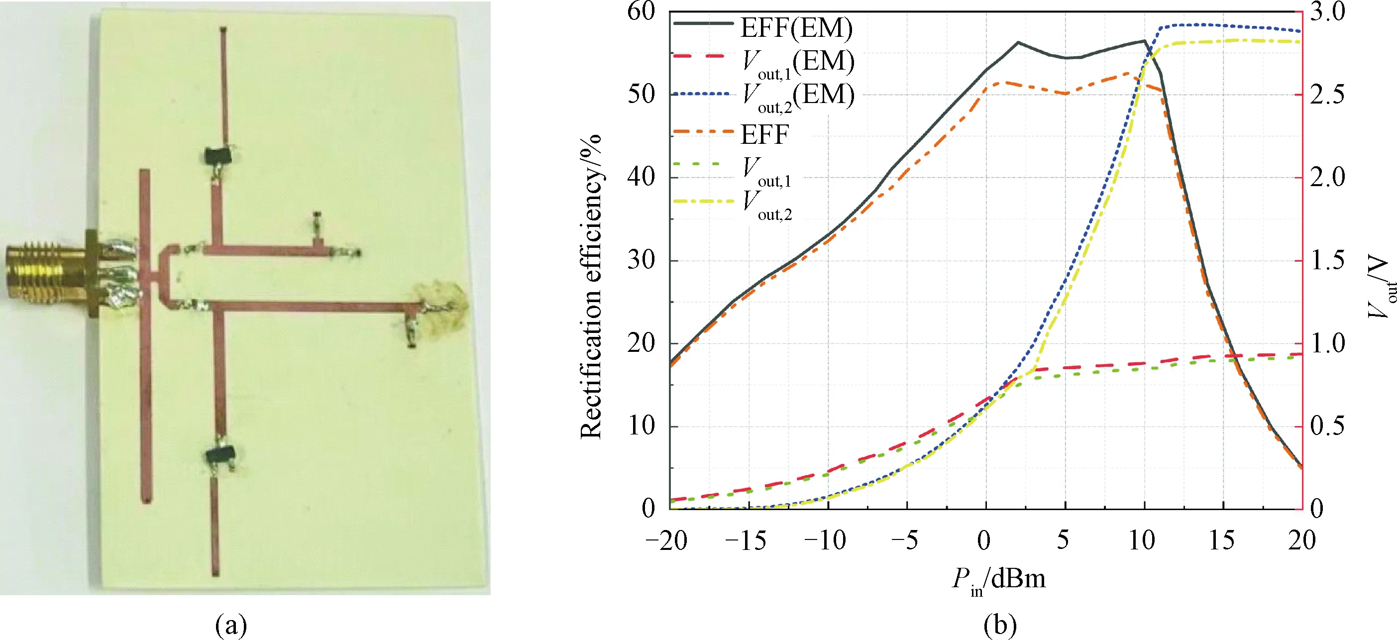
Fig. 11 Fabricated rectifier and test results:(a) physical diagram of rectifier circuit; (b) comparison between actual rectifier circuit efficiency and EM simulation results
4 Conclusions
A rectifier circuit with a wide input power range operating at 2.45 GHz frequency has been designed. The input power range was widened to a low power range below 0 dBm, and its main input power range was from -5 dBm to 12 dBm. At the same time, the input impedance of the rectifier circuit was controlled within a stable range by combining it with the impedance compression network. The future impedance of the receiving antenna can be set as the conjugate of the input impedance of the rectifier circuit to eliminate the impedance matching network and improve the rectifier efficiency.
杂志排行

Journal of Donghua University(English Edition)的其它文章
- TSCL-SQL:Two-Stage Curriculum Learning Framework for Text-to-SQL
- Unifying Convolution and Transformer Decoder for Textile Fiber Identification
- Optimization of Insulin Rapid Amyloid Fibrosis Conditions
- Data-Centric Approach to Digital Twin Modeling of Production Lines
- College Basic Development Status Data Management System Based on Data Governance Framework
- Complex Dynamics Analysis of Generalized Tullock Contest