Challenges and potential solutions of Ⅲ-nitride based Micro-LEDs
2023-07-17WaqarAZEEMLIUZhaojunFUGuiyue
Waqar AZEEM,LIU Zhao-jun*,FU Gui-yue
(1.Department of Electrical and Electronic Engineering, Southern University of Science and Technology, Shenzhen 518055, China;2.Institute of Physics, The Islamia University of Bahawalpur, Bahawalpur 63100, Pakistan)
Abstract: Micro-LED is considered as a crucial and one of the fastest growing display technologies in the world as it finds its applications in variety of products from visible light communication applications to large flat panel displays,virtual reality and wearable displays,televisions and light sources for the optogenetics and neural interface. Though the prospects are bright,Micro-LEDs still face some technological problems which needs to be addressed in order to get high volume commercialization,which include improving efficiency of LEDs with longer wavelengths,improving efficiency at low current densities,full color schemes,mass transfer,defects and yield management,repair technology and cost control. This review highlights the different challenges and their optimum solutions for Micro-LEDs.
Key words: Micro-LEDs; display technologies; efficiency of LEDs; mass transfer; Ⅲ-nitride
1 Introduction
In 1980s after the rapid development of GaN technology,different optoelectronic and power electronic applications were developed based on Ⅲ-nitride materials system[1-2]. From the time when it was first invented in 1992,InGaN based light emitting diodes (LEDs) have been one of the most significant and advanced devices among other applications of Ⅲ-nitride[3]. Ⅲ-nitride based LEDs are progressively being engaged as an energy saving solution for general lightening,automobile,signal and backlighting in displays because of the fact that they are reliable,efficient and have longer life spam as compared to other traditional lightening sources such as incandescent and fluorescent bulbs. Change in the format of LEDs from a standard size of 5 mm×5 mm for power LEDs for lighting and 300 μm×300 μm for indicators[4]to a micro-size of about 10~30 μm[5-6]has shaped a subfield in Ⅲ-nitride and display research and launched serious efforts in growth of Ⅲ-nitride devices and products. The development of micro light emitting diode (Micro-LED) is in good progress but the dimensions of Micro-LED are not defined clearly in literature and thus used in different applications depending on their sizes. We consider Micro-LEDs as LEDs having size less than 100 μm for estimation of recent developments in display and communication technologies[7]. Micro-LEDs find their application in visible light communication and near eye displays for virtual reality (VR)and augmented reality (AR)[8-9].
Organic light emitting diodes (OLEDs) and liquid crystal displays(LCDs) are the key contributors of today’s mainstream flat panel displays[10-11].Traditional LCD display suffer from the issues of low viewing angle,low uniformity,slow response time and high power consumption when it requires LED backlit to generate image by emitting a light through a matrix of liquid crystal. In contrast to LCDs,OLED displays are self-emissive and can be switched on and off independently. However,due to its organic nature,OLEDs has limitations in brightness and stability. Compared with them,Micro-LEDs displays possess potential advantages such as low power consumption,high contrast ratio,long lifetime and relatively wide color gamut.Micro-LEDs have attracted the attention of large number of academic researchers,manufactures and startups because of the prospects of their wide range of applications. Apart from display applications,Micro-LEDs have been explored to improve the luminescence efficiency for high-intensity lighting inspired by their lower self-heating effect,better current spreading and high light extraction efficiency[12-13]. Advanced research on Ⅲ-nitride LEDs began around 20 years ago[14],and enhanced efficiencies resulted in succeeding improvements for solid state lighting (SSL). The advancements include higher input powers,device designs for higher extraction efficiency,epitaxy and structural developments,and moving to larger chips[2,15]. The motivation of this article is to overview the technological developments and to shed light on challenges for Ⅲ-nitride Micro-LEDs to efficient microdisplays and to endorse future research in this area.
2 Bottlenecks and Solutions
Though,there are some technological developments,but when the chip density increases and the chip size contract,new technical challenges arises. To overcome these challenges,new methods have been developed from the current investigations.
2.1 Epitaxial growth and chip processing
Low defect density,wavelength and drive current homogeneity through the wafer are the main requirements for the epitaxial growth of GaN-based Micro-LEDs. To meet the requirements of large size Monolithic Micro-displays,there is a need of large diameter sapphire substrates,which produce some difficulties because of large thermal and lattice mismatches with the LED epilayer structure[16]. The main problem linked with the wafer bowing in InGaN/GaN MQWs is the nonuniformity of wafer’s surface temperature resulting in the spatially non-uniform distribution of indium molar fractions. A wavelength variation of 1.8 nm and 2.5 nm can be induced with a temperature variation of 1 ℃ in blue and green LEDs respectively[17]. During device fabrication,wafer cracking,degradation of device uniformity by dry etching and other similar processes are also caused by wafer bowing. To overcome these challenges,different solution has been employed,which include use of thicker substrates,control of coalescence stage,optimized wafer holding designs,internally focused laser treatment and the insertion of strain compensation layers[18-19]. Luet al. have shown that for 2,4,6 inch (1 in=2.54 cm) wafers the photoluminescence (PL) peak wavelength uniformity (with standard deviation of 2 nm) can be obtained,but not true for 8 inch wafer as the pocket design needs to be improved,as shown in Fig.1. In another study,Aidaet al. have reported that by using an internally focused laser processing,a reduction of bowing in GaN on sapphire and silicon substrates was observed[20]. As bowing act in opposite direction,so to compensate for the strain generated by GaN/sapphire system,a laser induced stress was applied near the backside of sapphire substrate,while for GaN/Silicon system stress was implanted near the interface of GaN and silicon.
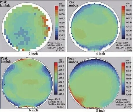
Fig.1 PL peak wavelength uniformity map for 2,4,6,8 inch wafers with zero edge exclusion. PL uniformity is very comparable,all around 2 nm in standard deviation except the 8 inch wafer due to nonoptimized wafer pocket design[16]. Reprinted with permission of Springer Nature,copyright (2010).
Spacing between devices and reduced size of Micro-LEDs can cause problem in chip processing and thus worsen the device performance. During device processing,high density of surface defects causes sidewall effect which leads to degradation in homogeneity,quantum efficiency and electrical injection in p-GaN[21-22]. The surface defects on the sidewalls act as non-radiative centers and thus degrade the quantum efficiency of Micro-LEDs.When chip size of Micro-LEDs reduced from 500 μm×500 μm to 10 μm×10 μm,then a decrease in external quantum efficiency from about 10% to 5% has been reported,as shown in Fig.2[23].The effect of size reduction on the performance of LEDs with large perimeter to area ratios is more noticeable. The peak quantum efficiency of less than 10% or even 1% was reported for LEDs with dimensions less than 5 μm[25]. Chenet al.have stated that a SiO2leakage current confinement layer in pyramidal Micro-LEDs can reverse the leakage current by two orders of magnitude,and thus improved the light output of Micro-LEDs by 115%[26]. Atomic layer deposition (ALD) of SiO2for sidewall passivation can reduce the sizedependent factors on peak external quantum efficiency (EQE) of Micro-LEDs[27]. The EQE of 20 μm×20 μm Micro-LEDs can be increased from 24% to 33% with the help of ALD passivation. Oliveret al. have improved the EQE of 10 μm pixel pitch Micro-LEDs from 4.8% to 6.8% and obtained a brightness of 107cd/m2by changing the p-contact metal from Ni-based to Agbased and mesa etching process formation between p-contact and hybridization pad into a softer plasma[21]. It has been reported by Hwanget al.that the peak EQEs of 48. 6% and 40. 2% can be maintained for a chip size of 100 μm×100 μm and 10 μm×10 μm respectively[22].
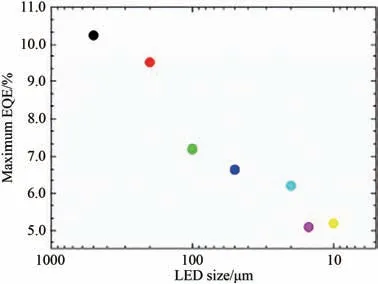
Fig.2 Effect of size reduction on the EQE of GaN-based micro LEDs [24]
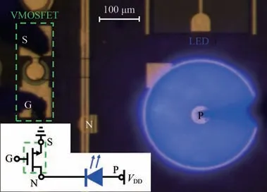
Fig.3 Optical representation of monolithically integrated VMOSFET LED device with equivalent circuit design [28]. Reprinted with permission of AIP publishing,copyright (2016).
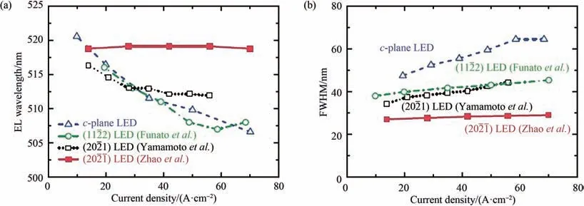
Fig. 4 Optical characteristics of semi-polar (202ˉ1ˉ) green LEDs,where (a) peak wavelength and (b) FWHM curves as a function of current densities [38]. Reprinted with permission of The Japan Society of Applied Physics,copyright (2013).
2.2 Full and hybrid monolithic micro-displays
Fully monolithic active matrix micro-displays can be developed by incorporation of individual GaN-based LED driven by a GaN based transistor for each pixel,because Ⅲ-nitrides are exceptional materials for both LEDs and high frequency and high power transistors. Lauet al. have reported the fabrication of InGaN/GaN LEDs integrated monolithically with vertical metal oxide field effect transistor (VMOSFET) drivers[28]or AlGaN/GaN heterojunction field effect transistors (HFETs)[29],by selective growth of HFET or VMOSFET structures on the LED epilayers as shown in the Fig. 3. On the other hand,on top of the exposed n-GaN layer,selective removal of the LED structure followed by the selective growth of the metal oxide field effect transistor (MOSFET)[30]or selective removal of the HFET structure followed by the selective growth of the LED structure on top of the GaN buffer layer have also been reported[31].While it has been reported that the performance of the integrated single LED transistor chip is comparable to discrete LEDs,but by using this approach the transistors fabrication of Micro-LEDs has not been reported yet[29].
In full monolithic integration there are difficulties and incompatibility between the Micro-LED and driver IC process,so the hybrid monolithic integration is the most common approach implemented by the Micro-LED display developers.Fabrication of Ⅲ-nitride based Micro-LED arrays,manufacturing of Si-based CMOS driver matrix,and then their hybrid integration to allow control of the LED pixels individually use monolithic hybrid approach. The hybridization process which has been extensively developed in Ⅲ-Ⅴ/Si photonics for high performance switching and computing is generally based on flip-chip bonding technology[32]. Dayet al. have presented the fabrication of a 160×120 VGA micro-display with a pixel pitch of 15 μm by using 6 μm sized indium metal bumps deposited on Micro-LED pixels as bonder[33].
Apart from above mentioned monolithic fabrication processes,it has been reported that the Micro-LEDs display can be realized without the need of mass transfer by using GaN based nanowire Micro-LEDs. A wafer to wafer transfer technology has also been employed by “Glo-USA Inc” to construct 1.5 inch 264 PPI RGB wearable display using 20 μm sized Micro-LEDs on a LTPS gas backplane,and a 0.7 inch 1 000 PPI RGB display using 10 μm sized Micro-LEDs on a CMOS backplane.
2.3 Realization of full color format
Full colors (red,green and blue) for each pixel are needed for most of the micro-display applications. In LCD display technology,LED backlight is used to generate light through a matrix of liquid crystal ‘light switches’ and color filters creating the individual subpixels. Whereas in Micro-LED display,each subpixel is based on matrix of tiny light emitters made of Micro-LEDs and the brightness of each subpixel can be controlled individually. However,similar to other hetero junction based semiconductor structures,Ⅲ-nitride LEDs being a monochromatic light sources emit light at a single color,with its wavelength determined by the indium content in InGaN/GaN multiple quantum wells (MQWs). Despite numerous approaches to harvest full color micro displays from single color Micro-LEDs,it still remains to be a challenge for developers.
For a full color format,the most common approach is to assemble discrete commercial LEDs with the three different colors to form an array with each pixel holding red,green,and blue(RGB) LEDs. In theory,by changing the indium content in InGaN/GaN MQWs all these three colors can be generated. Unfortunately,large lattice mismatch between the active InGaN layer and GaN buffer results in low luminescence efficiency for InGaN based red and green LEDs. This restricts the progress in developing full-color displays using GaN family alone. GaP/GaAs based LEDs can be used to emit red light,but as the size shrinks it may suffer from even more substantial drop in EQE[22]. With the peak EQE values of more than 50% in blue and green,the InGaN LEDs on polar c-plane orientation have shown extraordinary performances among the three primary colors. On the other hand,red InGaN LEDs demand more optimizations and improvements in terms of peak EQE and optical characteristics[2,34].
In order to obtain longer wavelength emission for InGaN LEDs,several approaches including relaxed InGaN pseudo-substrates (InGaNOS) and semi-polar GaN templates have been developed for more indium incorporation in active region. To realize RGB emission by PL,Evenet al. has reported a full InGaN heterostructure grown on In-GaNOS with different lattice constants[35]. Using InGaNOS technology,100 μm×100 μm LEDs has generated a red emission wavelength at 630 nm,but the maximum EQE was very low[24]. Alternatively,the advantages of semi-polar orientations including small blue shift in wavelength and low efficiency drop with increasing current density for typical optoelectronic devices have been observed experimentally[36-37].
Zhaoet al. has demonstrated a blue shift in wavelength and narrow FWHM of a semi-polar(202ˉ1ˉ)green LEDs fabricated on a free standing semi-polar GaN substrate as shown in Fig.4. Free standing semi-polar GaN substrates ‘prepared by hydride vapor phase epitaxy (HVPE) or ammonothermal growth’ are used for the growth of optoelectronic devices including LEDs and laser diodes[37,39].Conversely,the devices which use bulk GaN as a substrate are limited by substrate dimensions and are currently too expensive for display applications[40]. The optical and electrical properties of green Micro-LEDs fabricated on semi-polar(112ˉ2ˉ)GaN/sapphire templates are reported by Liet al.[41].For solid state lightening purposes,AlGaInP LEDs are highly energy efficient,so with the developments towards red InGaN Micro-LEDs,AlGaInP serves as an another material system for red emission[42]. Sidewall defects and surface recombination velocity are the key issue with AlGaInP materials,and because of these problems their performance drop significantly as the device dimensions shrinks[43-44]. To realize full color displays,besides RGB self-emissive Micro-LEDs,monolithic blue or UV-A Micro-LEDs with color conversion materials is also an attractive method[45-46].
Because of the high thermal and chemical stability and outstanding quantum yield,phosphors have been frequently used to produce white light for solid state lightening. However,they are typically in micron scale which is equivalent or larger than the size of Micro-LEDs,so the problems of light scattering and light inhomogeneity need to be overcome[24]. In the same way,quantum dots are an alternative option because of their excellent quantum yield,nanoscale sizes,narrow FWHM and controllable wavelength emissions[45,47]. By using nanoring Micro-LEDs and CdSe/ZnS red quantum dots,Chenet al. have used a hybrid approach to form RGB pixels on the same substrate[24]. Their results displayed maximum wavelength emissions at 630 nm,525 nm and 467 nm with 78.2% color gamut overlap of Rec. 2020 as shown in Fig.5.
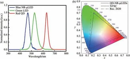
Fig.5 Optical performance of NR-Micro-LEDs and quantum dots.(a) EL spectra of RGB colors; (b) Color gamut of RGB hybrid QD NR Micro-LEDs,NTSC,and Rec. 2020 [45]. Reprinted with permission of Optica Publishing Group,copyright (2019).
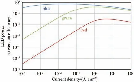
Fig.6 Plot of power conversion efficiency against current density for the red,green and blue LEDs[44].Reprinted with permission of John Wiley and Sons,copyright (2019).
The problem of low power conversion efficiencies for green and red emitting LEDs is known as “green gap”[48-49]. Green gap usually occurs for a display consist of entirely Ⅲ-nitride LEDs. The green gap can be seen in Fig. 6 where power conversion efficiency is plotted against current density.With the increase in current densities,the power conversion efficiencies of the LEDs decreases and with the increasing operating wavelength from blue to red,the peak efficiency shifts to higher current densities. The efficiency of all three colors ultimately decreases at higher current densities due to auger recombination. In InGaN QWs the wavelength can be increases by increasing the indium content.This decrease in efficiency by increasing the indium content has many reasons[49-50]. A greater need for an effective blue SSL emitter is a main reason for the lack of performance for red and green emittingⅢ-nitride LEDs over the last decade[49].
Among different solutions for higher efficiency green and red Micro-LEDs,it is difficult to calculate which solution will ultimately lead to the highest efficiency of Micro-LEDs display. The use of AlGaN interlayer in the MQW active layer is a good approach for higher efficiency longer wavelength InGaN LEDs which has produced some significantly improved efficiencies at green gap wavelengths[51-52]. This has revealed a record external efficiencies of about 25% at 550 nm[52]and 2.5% at 608 nm for green and red emission respectively. Fig.7(a) shows AlGaN interlayer grown on top of the InGaN QW. The benefits of interlayer include the capping of QW to retain indium,strain compensation to control defect formation,and the reduction of defects due to high temperature growth of the GaN barrier. The interlayer compensation for InGaN QW is shown in Fig. 7(b). The pseudomorphic growth of MQW can be made possible with interlayer by adjusting the Al composition and thickness. It can be seen in Fig.7(c,d) that the variation in strain of MQW with interlayer thickness is nearly pseudomorphic at an interlayer thickness of 1 nm[53]. Single digit efficiencies at longer wavelength specially in red can finally be realized for LEDs with interlayer based MQWs[54]. Further optimization of interlayer layer design could lead to further improvements.As it has been reported that AlInN can also be used as an interlayer and the efficiency gain produced is similar to that of AlGaN interlayer[53].
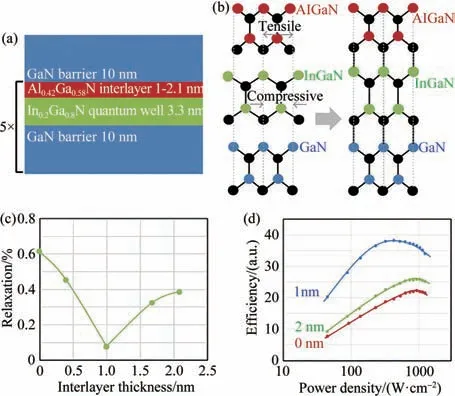
Fig.7 (a) Schematic cross section of a MQW with GaN barriers,AlGaN interlayers,and five periods of InGaN quantum wells; (b) 2D ball and stick representation of different layers; (c) Interlayer thickness versus relaxation plot ;(d) Power density versus efficiency plot showing that 1 nm thick interlayer has the highest efficiency[44]. Reprinted with permission of John Wiley and Sons,copyright (2019).
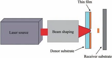
Fig.8 Schematic of LIFT off process[70]. Reprinted with permission of Elsevier,copyrigt (2016).
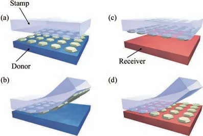
Fig.9 Schematic representation of steps involves in elastomer stamp micro-assembly process. (a) Prepare donor substrate; apply rubber stamp; (b) Quickly peel back stamp with objects attached with it;(c) Apply inked stamp to receiving substrate,and (d) with printing object on receiver substrate slowly peel back stamp [78]. Reprinted with permission of Springer Nature,copyright (2005).
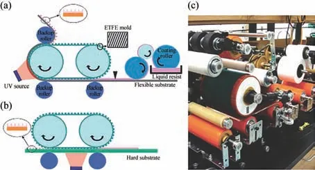
Fig. 10 Schematics of(a) roll to roll NIL and (b) roll to plate NIP process. (c) Photograph of 6-inch capable R2R/R2PNIL apparatus [76]. Reprinted with permission of American Chemical Society,Copyright (2009).
2.4 Pixel yield of the display
In an RGB full color high definition display(1 920 pixel×1 080 pixels) to preserve the dead pixel number less than 5 the yield should be 99.999 9%,which is difficult to achieve. During the fabrication process a dead pixel can appear in different stages,such as epitaxy,LED ship and transfer process. For example,during a monolithic fabrication of Micro-LED array by flip chip bonding,a large number of dead pixels are formed due to physical disconnection from p-electrode line triggered by severe bonding failures[55]. Apart from this,the yield of the display can also get reduced because of photoresist residue inside the gaps between LED elements[56]. Without using O2based plasma ashing step,for arrays with 170 μm gaps between mesas,the Micro-LED element yield is about 90%,and this yield further drops to 67%when the gap width is reduced to 6 μm.
Removing the photoresist residue by using plasma ashing step,the yield can be improved to 100% and over 95% for 170 μm and 6 μm gap arrays respectively. A repair process is inevitable for a zero dead defect display,even supposing an extremely high yield. Increasing the redundancy by doubling the number of Micro-LED element for each pixel can be a simple solution. However,the initial defective yield controls the effectiveness of the built-in redundancy. If the yield is 99.99%,then by doubling the number of Micro-LED,the number of dead pixels can be reduced from 5 000 pixel to 5 pixels in a fully high resolution display,but a pixel yield of 99.9% will still keep the number of dead pixels up to 500[57]. Since,Micro-LEDs with double number are used,so the cost of the display will be enhanced greatly.Although some developers have suggested an individual pixel repair technology,but this approach is expensive and cannot be applied to displays prepared by monolithic fabrication.
2.5 Working at low current densities
The required output power of Micro-LEDs depends on the display variables such as the screen luminescence(cd/m2) and pixel density(ppi). For each color,current densities and efficiencies will determine this output power. The pixel density decreases while increasing the viewing distance,that’s why the TV display has a lower pixel density than a mobile phone. Display environment and its use determine the screen luminescence,for example because of outdoor use,the screen luminescence of a watch is higher than a TV (1 000 cd/m2versus 500 cd/m2). Here we will discuss the operating points for displays with pixel density (500 and 1 000 ppi) and having lower values for luminescence (102~104cd/m2),and micro-displays having pixel density(2 000 and 5 000 ppi) with higher values for luminescence (103~105cd/m2). The comparison of efficiency for red,green,and blue Micro-LEDs at different current density with a pixel density of 500 and 1 000 ppi shows that the operating points shifts to a peak efficiency with greater luminescence[44]. Red and green subpixels operate at higher current densities than the blue to overcome the lower efficiencies.
For short viewing distance micro-displays such as the AR and VR,the efficiency against the current density of red,green and blue Micro-LEDs at a pixel density of 2 000~5 000 ppi with screen luminescence of 103,104,105cd/m2,and die spacing of 1 μm has been observed[44]. An increase in operating point has been noticed with the increase in pixel density and luminescence. The motivation is to reduce the area and LEDs for a luminaire by constructing the LEDs which can operate at higher current densities. Auger recombination is of great distress in SSL where the operating current densities are high,but for Micro-LED display and micro display,the operating points are just above or below to a peak efficiency and are at much lower current densities. Consequently,auger recombination is not a big problem for Micro-LEDs for both type of displays. The ratio of spontaneous to defect combination rates have more influence on the efficiency of Micro-LEDs,and for future gains,increasing this ratio is of great importance. Having great importance for SSL,defect recombination should be even a more substantial focus for Micro-LEDs.
Different approaches can be taken to shift the peak efficiency at the operating points. L. Wanget al. have reported a higher external quantum efficiency(18.2%) at extremely low current density(0.5 A·cm-2) for Micro-LEDs based on InGaN quantum well. They have used Stranski-Krastanov(SK) and Volmer-Weber (VW) modes to selfassembled InGaN quantum dots by using metal organic vapor phase epitaxy[58]. These results suggest that InGaN quantum dots can give an ideal solution to Micro-LEDs for display and VLC applications. Reduced current injection area of LEDs is one of the option,but for Micro-LEDs one could increase the operating current density nearer to peak efficacy by reducing the area. Patterning off some of the active layers by using smaller contacts or implantation to create deadened region can also be employed to control the total area. Lit area can also be controlled by using nanowire geometries[59-60].Use of pulse width modulation (PWM) system is another trick to control the operating point of Micro-LED. By controlling how often an LED is turned on,PWM is used to manage the luminescence of the screen,and one does not have to worry about shifts of colors with the current as PWM sets the current and efficiency. Conversely,PWM could also be used to control the operating points to a more effective position if one could also increase the peak current beyond what is necessary for luminance[61].
2.6 Mass transfer
For a full color or flexible Micro-LED displays,mass transfer of Micro-LEDs with approximately perfect yield and selectivity is also a critical challenge. Because of large quantity of RGB Micro-LEDs and their tiny nature,the present transfer techniques are difficult to use to realize a cost and time effective manufacturing process with arduous pixel control and yield requirements[62-63]. For wearable and bioelectronics applications,flexible and stretchable optoelectronics have gained substantial research popularity recently,and this requires the transfer of inorganic LEDs onto flexible substrates[64-65]. Unlike OLEDs,rigid substrates like sapphire and silicon have been used to grow inorganic LEDs,and thus for flexible application it requires transfer of LEDs from originally grown substrates to another substrate[66-67]. Despite the fact that there exist several substrate removal techniques for different semiconductors,but unlike AlGaInAs,InGaN material system lacks the damage free and high selectivity etching methods,and this adds challenges to remove devices for mass transfer[68-69]. Transfer rate is one of the key parameters to determine the practical usefulness of different transfer techniques. Laser induced forward transfer (LIFT),fluidic assembly,elastometric stamp,roll to roll stamping and electrostatic array are some most useful transfer methods.
In laser induced forward transfer (LIFT) process,a laser beam is used to separate the Micro-LEDs from their carrier substrate and then transferred to a receiver substrate as shown in Fig. 8[70].This process also be employed by using a temporary substrate with a polymer adhesive acting as an interfacial layer,which decomposes when irradiated with a laser beam. LIFT technology is reported to allow 1 000 chips to be transferred per laser shot.It has been reported that a massively parallel laser enabled transfer technology can have a transfer rate of 1×10⁸/h[71].
Mass transfer of LED ships by fluidic assembly process has also been investigated. In this process,gravity and capillary forces have been used to drive and capture the Micro-LEDs on to the array of driver ICs[72-73]. Fluids like distilled water,acetone or isopropanol can conduct the self-assembly.
It was reported that by using fluidic assembly method a transfer rate of 50 million devices per hour can be obtained[74]. Electrostatic array technology operates in accordance with the electrostatic principle and pick the Micro-LEDs by the attraction of opposite charges[75]. This process uses an array of electrostatic transfer heads to pick up an array of Micro-LEDs from a carrier substrate. A grip pressure is generated with a pull in voltage from a working circuitry,then by applying transfer heat from the head,the bonding layer on the receiver substrate is liquefied. Thus,a Micro-LED is released to the receiver substrate by bonding an array to a receiving substrate.
Fig. 9 shows in elastomer stamp micro assembly technology,native wafer substrates are prepared to supports the completely formed,organized arrays of Micro-LEDs. Then Micro-LEDs are attached to a soft elastomer stamp with a high peel velocity. Rate dependent adhesion forces of stamp which are controlled by van der Waals interactions are used to lift the Micro-LEDs from native substrate. After that Micro-LEDs are released from the stamp with a sufficiently low peel velocity,and then transferred to a receiving substrate. By this technique a transfer rate of 1×10⁶/h can be achieved.
For high speed large area nanoscale patterning,a continuous roll to roll nanoimprint lithography (R2RNIL) technique can offer a solution with significantly improved output; moreover,in large area imprinting the challenges faced by conventional NIL in maintaining pressure uniformity and successful demolding can also be solved with the help of R2RNIL[76]. Korean Institute of Machinery and Materials (KIMM) have developed a roll to plate transfer process[77],by using this technique Micro-LEDs with chip size and chip thickness less than 100 μm and 10 μm respectively,can be transferred. For a flexible,stretchable and lightweight displays,this technique can provide a transfer rate up to 10 000 devices per second. Fig.10 shows the overall configuration of a continuous (a) roll to roll NIL and (b) roll to plate NIP nanomanufacturing process,which involves two steps: (1) the coating process,in which liquid phase UV-curable resist material is constantly coated on either flexible PET or glass substrate by a three step roller coating system,(2) the imprinting curing process,where the coating system is synchronized with the main imprinting roller to assure uniform coating thickness.
2.7 Requirements of device designs
Highest pixel densities are required for tiny devices with length scale of 10 μm. These dimensions are smaller by an order of magnitude as compared to that used in standard Ⅲ-nitride LEDs. Simple lithographic tools can be used to achieve a significant (5 μm or above) offsets between mask layers and tolerances between levels for standard LEDs.But,more refined lithographic tools are required for Micro-LEDs that will implement other improvements such as flat and lower defect density wafers. P. Liet al. demonstrated that the packaged Micro-LEDs show a peak external quantum efficiency ranged from 2.4% to 2.6% as the device area reduces from 100 μm×100 μm to 20 μm×20 μm[79]. These results show that by using InGaN materials,a very small size red Micro-LEDs with high efficiency can be obtained. Surface recombination becomes a problem particularly for devices with smaller size as one uses traditional layered epitaxial structure and device fabrication processes[12]. Power conversion efficiency versus current density for a green LED with a chip of squared shape is shown in Fig. 11(a). A surface recombination velocityvs=6×103cm·s-1found on m-plane bare surfaces is the worst case[80-81].
For a Micro-LED the device dimensions are very small so it is important to include surface recombination rateRsr,which can be expressed aswhereasis the exposed surface area,Vis the active region volume andvsis the surface recombination velocity[82]. Surface recombinationasVincreases from 4×101cm-1to 4 ×104cm-1with a decrease in chip area. This results a significant decrease in efficiency at low current densities as shown in Fig.11(a). For a green LED with constant length of 5 μm andvsfrom 1×104cm·s-1to 2×104cm·s-1,the external quantum efficiency versus density is shown in Fig. 11(b). The surface recombination needs to be almost nonexistence in Micro-LEDs as the low current density only recovered atvs=1 cm·s-1in this configuration. Low coupling efficiency of the LED at the view angle is another challenge,and this can be overcome if one could control the Micro-LED radiation pattern,which results in increased total efficiency. Micro-LEDs would need to be picked and placed into a package or into a backplane in case of emissive display,if one follows the traditional LED fabrication process[83]. As for small LEDs,placement process is very challenging,so one option is to find such pathways to avoid this pick and place method.
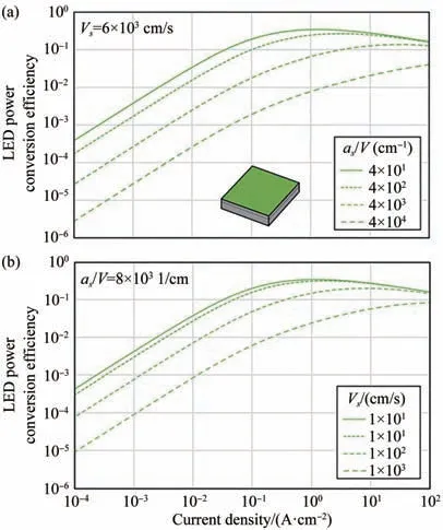
Fig.11 Plots of current density against power conversion efficiency for green LED. (a) Constant v=6×103 cm·s-1 and variable as/V=4×101 to 4×104 cm-1;(b) Constant as/V=4×104 cm-1 and vs=1,10,100,1 000 cm·s-1[44]. Reprinted with permission of John Wiley and Sons,Copyright(2019).
To ensure high efficiency operation of Micro-LEDs their device and system challenges need to be addressed. We will disclose some methods to solve these challenges which include controlling the radiation pattern,controlling the surface recombination,and use of monolithic growth approach to avoid pick and place. Etching[84]and passivation methods can be used to lower surface recombination[85]. Alternatively,to block the current from the edges of the die,epitaxial growth on the exposed surface or implantation or oxidation techniques[86]can be used as done in other Ⅲ-Ⅴsemiconductors. Use of different structures such as core/shell nanowire configuration is another possibility[87]. In this approach,recombination take place near to the top of the nanowire,far from the exposed QW at the bottom of the wire as the QW is generally buried in this case[87].
Use of photonic crystals with LEDs is one of the methods to control the radiation pattern to increase coupling efficiency. The control of emission pattern through scattering can be achieved by placing a photonic crystal or on top of an LED[88].LED areas can be affected by diffraction lengths and their impact on emission patterns. Nanowires can be used as an alternative method as they are patterned systematically and also diffracts light[87].Lastly,vertical cavity surface emitting laser can also be an option[89]. As these coherent sources have small emitting apertures,their light can be easily directed into the viewing angle,and can be arrayed easily,so they are attractive for displays.
In case of a high luminance and high pixel density micro display,extremely small devices with side dimensions of <10 μm and spacing <2 μm are necessary. Assuming the small size of Micro-LEDs,it is beneficial to avoid pick and place methods.Epitaxial growth of all colors simultaneously is a one solution. Site controlled growth can be used to grow all three color successfully,in which indium incorporation is determined by confinement[90].Nanowires structures has also been produced by using this monolithic approach[59]. Alternatively,by using multiple epitaxial steps,selective area epitaxy can be used to integrate active layers of different colors as it has been used in other Ⅲ-Ⅴsemiconductors to create photonic integrated circuits[91]. Time will determine the validity of these difficult growth approaches to produce efficiencies that can strive with traditional LED structures.
3 Machine Learning for Micro-LEDs
Theoretical models based on computer simulations can be tested by comparing the calculated results of experimental measurements. Thus,simulations can help to explain the experimental results that are difficult to understand. As mathematical tools always make the reality simpler,so it is well established that the initial simulation results barely agree with measurements. Therefore,to find an agreement between theory and reality,a careful tuning of computer simulations are required[92]. On the other hand,machine learning usually performs statistical analysis on the data collected from real world as shown in Fig.12. This statistical analysis is valuable when the amount of data is very large and hard to digest.
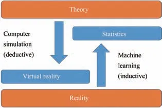
Fig.12 Computer simulation versus machine learning[93].Reprinted with permission of Springer Nature,Copyright (2021).
From machine learning methods,deep learning is most popular for the analysis of large amount of data and it is based on multi layered artificial neural networks[94]. Large amount of data sets is needed to train an artificial neural network.Computer simulations based on established theories are used to collect experimental data as real world data is difficult to collect because it is insufficient and scatter. Such physics based machine learning models are increasingly employed in materials science[95]. Many semiconductor material systems are discovered and optimized for applications in optoelectronics[96-97]. Different optoelectronic devices have been analyzed by using simulation based machine learning technique[98-99].
Machine learning can also be used to improve the performance of Micro-LEDs. Classical approaches for light emitting surface characterization results in an underestimation of actual Micro-LED array behavior as they cannot distinguish between functional and defect pixel. The existence of nonfunctional Micro-LEDs in a Micro-LED array creates a problem in the development process. Noise created by the defect pixels also cause a problem in the evaluation of design change. Therefore,to overcome this blurring effect,each pixel should be classified and may not be considered for the final analysis. Spatially resolved measurements of color/luminance of single Micro-LED and the whole light emitting surface are examined as they are essential for the development of visual insight. However,the former take lot of time in measurements and evaluation,and the later undergoes interference produced by nonfunctional Micro-LEDs.Steven Becker in his article used an unsupervised machine learning model to perform both of these analysis in a single measurement. The results shows that a precise reconstruction of Micro-LEDs and more accurate characterization of Micro-LED arrays can be performed by employing a machine learning technique[100].
However,as the current model uses unsupervised learning (KMeans),it could act differently on different Micro-LED arrays. Switching to a supervised machine learning model (Random Forest)could support the robustness of the analysis,but this requires a labeled data set,which is again a time taking process. This suggest that employment of measured data increases the validity of machine learning models for the performance analysis of Micro-LEDs.
4 Conclusion
The display technology has been improved significantly with the development in GaN based materials system. Micro-LEDs have gained substantial research attention as they yield attractive benefits for next generation display and data communication applications. The performance of Micro-LEDs is influenced by different factors such as surface recombination,green gap and low coupling efficiencies into the display viewing angle. The development of Micro-LEDs and solution to different challenges have been reviewed. The significance of full color scheme and mass transfer techniques has also been revealed. The combine efforts from the R&D groups of Ⅲ-nitrides LEDs,optogenetics and display will empower the Micro-LED technology to flourish to serve society at largest scale by overcoming the technical challenges.
