A self-driven photodetector based on a SnS2/WS2 van der Waals heterojunction with an Al2O3 capping layer
2023-02-20HsiangChunWang王祥骏YuhengLin林钰恒XiaoLiu刘潇XuanhuaDeng邓煊华JianweiBen贲建伟WenjieYu俞文杰DeliangZhu朱德亮andXinkeLiu刘新科
Hsiang-Chun Wang(王祥骏), Yuheng Lin(林钰恒),Xiao Liu(刘潇), Xuanhua Deng(邓煊华),Jianwei Ben(贲建伟), Wenjie Yu(俞文杰), Deliang Zhu(朱德亮), and Xinke Liu(刘新科),†
1College of Materials Science and Engineering,Institute of Microelectronics(IME),Guangdong Research Center for Interfacial Engineering of Functional Materials,Shenzhen University,Shenzhen 518060,China
2State Key Laboratory of Functional Materials for Informatics,Shanghai Institute of Microsystem and Information Technology,Chinese Academy of Sciences,Shanghai 200050,China
Keywords: SnS2/WS2 heterogeneous junction,Al2O3 layer,self-driven,photodetector
1. Introduction
Since the discovery of graphene, two-dimensional (2D)materials have been considered as promising candidates to replace silicon-based optoelectronic devices because of their high flexibility, excellent carrier transmission and designable interface characteristics.[1–5]However, graphene is limited in many fields due to its zero bandgap. As substitutes for graphene, 2D transition metal dichalcogenides (TMDCs)are two-dimensional semiconductor materials that have been widely studied.[6–10]The transition metal sulfide molecular formula isMX2(M= W, Sn, Mo, etc., andX= S, Te or Se), and the molecular structure is the sandwich-like structure ofXMX. Compared with graphene,TMDCs have an adjustable bandgap of 1 eV–3 eV, which makes them suitable for the preparation of photodetectors, solar cells, FETs and gas sensors, etc.[11–22]In particular, TMDCs have the potential to achieve high-efficiency photodetectors due to the high absorption coefficients in the ultraviolet and visible regions.SnS2has an indirect bandgap of~2.3 eV, which is stable with the change of thickness.[23,24]It has been reported that the carrier mobility of a SnS2based ultra-thin transistor was about 50 cm2/(V·s) and a high onoff current ratio of 106has been achieved, thus making SnS2a favorable material for the fabrication of photodetectors.[25]It has been reported that an ultraviolet (UV) to near-infrared (NIR) photodetector based on a SnS2nanosheet and microsphere film have been achieved, showing remarkable performance.[26,27]Tungsten disulfide (WS2), one of the TMDCs, is a potential candidate for various electrical and optical applications due to its large and distinctive tunable bandgap (1.3 eV–2.1 eV).[28]When the thickness of WS2decreases to a single layer, the band structure of WS2will transform from indirect to direct.[29]The carrier mobility of 2D WS2has been reported as high as 232 cm2/(V·s). The band structure of 2D WS2shows relatively large valence band splitting compared with other 2D TMDCs materials, which makes the Hall effect easier to observe.[30]In addition, WS2can be used as a lubricant in a wide range of operating temperatures, which is attributed to its high thermal stability.[31]However, SnS2based detectors have a low operating speed, and the existence of surface defects is one of the causal factors.[23,32,33]To solve the problem, the surface passivation method has been adopted. It has been reported that the surface of 2D SnS2material can be passivated to reduce surface defects, decrease response time and improve the responsivity.[12]Meanwhile,high-sensitivity photodetectors based on WS2can also be realized through interface passivation.[34]
The development of energy saving and environmental protection devices is the general trend. Under this background, one of the main challenges for the next generation of photodetectors is to reduce the overall power consumption. As a result, self-driven photodetectors are increasingly attracting attention.[35–37]Compared to conventional photodetectors, self-driven photodetectors exhibit ultra-low dark current and noise, resulting in a very high signal/noise ratio. From this viewpoint,self-driven photodetectors are confirmed to be the best candidates for the next generation of photodetectors.[37,38,43]Combining the advantages of 2D materials, self-driven photodetectors based on 2D material heterogeneous junctions have been reported.[44–46]For example,a photodetector based on a monolayer MoS2/WS2heterojunction structure has shown good performance with responsivity of 4.36 mA/W and detectivity (D*) of 4.36×10¹³Jones under 532 nm wavelength.[45]It has been reported that visible phototransistors based on nanolayered heterostructures of SnS/SnS2and SnSe2/SnS2show very high photoresponsivity of 3567 A/W and 1793 A/W, respectively.[46]However, heterostructure photodetectors with excellent self-driven performance and good rectification effectively prepared by other 2D materials urgently need research. Therefore, SnS2has a suitable bandgap and better optical absorption characteristics,but the higher photosynthetic electron–hole composite leads to a slow response time in the device, limiting its application in the field of photodetectors. WS2demonstrates excellent optical response performance, and also has higher electron mobility due to its smaller electron effective mass. In this work,a SnS2/WS2van der Waals heterojunction photodetector has been fabricated on a SiO2/Si substrate. As reported, depositing a surface passivation layer reduces the surface defects of the materials and introduces tensile stress to modify the intrinsic properties.[12,34]Furthermore,the device designed with 3-nm-thick Al2O3as a passivation layer and stress liner on the surface demonstrates better self-power and photoelectric detection performance than the initial device. The photodetector shows good detection,and the photoresponsivity of the device has been increased four times by covering the Al2O3layer. Under illumination of 365 nm and 0 V bias voltage,the SnS2/WS2photodetector with the Al2O3modified layer exhibits high photoresponsivity of 4.57 A/W and detectivity of 8.07×10¹⁰Jones(input power of 11.10 nW), which demonstrates relatively good self-power and high photo-responsivity performance. These results therefore provide an idea for the next generation of photodetectors.
2. Experimental details
Firstly,WS2crystals were mechanically peeled and transformed by adhesive tape onto the insulating Si wafer (with 300 nm SiO2on the Si surface). The WS2nanosheets with a thickness of about 10 nm were found using an optical microscope, and the specific location was marked. Then, the SnS2was transferred to the PDMS film via the same mechanical stripping process. Under the optical microscope,the target SnS2was transferred to the target WS2to construct the SnS2/WS2heterojunction. Then, electron beam exposure(EBL, Raith EBPG 5150, Pioneer 2) was used to write the electrode pattern,and a thermal evaporator(ASB-EPI-C6)was used to deposit the titanium/gold (5 nm/50 nm) electrode to prepare the devices. Finally, a 3-nm-thick Al2O3passivation layer(stress liner)was grown on the surface of the SnS2/WS2heterogeneous structure at 300°C by an atomic layer deposition (ALD) process using trimethylaluminum (TMA1) as the precursor.
3. Results and discussion
The self-driven photodetector is fabricated based on the SnS2/WS2heterogeneous junction in this work. A schematic diagram of the heterojunction photodetector is shown in Fig. 1(a) and the preparation procedure is introduced in Section 2. The SnS2/WS2heterogeneous junction was illustrated by optical microscopy,as presented in Fig.1(b). Atomic force microscopy(AFM)is used to characterize the morphology and structure,figure 1(c)is the height profile across the edge of the heterojunction region and the inset is the AFM image of the location. Confirmed by AFM, the thicknesses of the SnS2and WS2layers are about 60 nm and 10 nm,respectively. The Raman spectra of SnS2,WS2,and the heterostructure regions are plotted in Fig.1(d). The Raman spectra were applied to confirm whether the WS2and SnS2layers were effectively transferred by comparing the spectra before and after transfer. The spectrum of isolated SnS2(red) shows one dominant peak at 314.1 cm-1attributed to the out-of-plane A1gmode. The Raman spectra of individual WS2(blue)have two typical peaks located at 350.2 cm-1and 420.8 cm-1that can be attributed to the in-plane E12gphonon mode and the out-of-plane A1gmode,respectively. The Raman peaks of the heterostructure region(black)exhibit the characteristic vibration modes of both SnS2and WS2; no obvious peak shift was observed in the heterojunction area, indicating that the high quality of the two materials remains in the junction region after transfer. From the spectrum, it can be concluded that the two-dimensional layered materials were transferred and almost no defects were induced during the transfer process.
By considering the band structure and the thickness of SnS2and WS2,[29,47]an energy band alignment diagram of the SnS2/WS2heterogeneous junction is presented in Figs. 2(a)and 2(b). The electron affinities of WS2and SnS2are nearly matched, which makes the SnS2/WS2heterogeneous junction suitable for design and fabrication as photodetectors.The photogenerated carriers can be well separated in the depletion region due to the existence of ΔEc, and the electrons can be smoothly transported because there is almost no electronic barrier in the conductive band. As a result, the SnS2/WS2-based heterogeneous junction presents self-driven performance. In our previous reports, the Al2O3layer can be used to improve the performance of photodetectors,which is also applicable in this work.[12,48,49]Figure 2(c) exhibits the comparative Raman spectra of the SnS2/WS2heterogeneous junction region and the heterostructure with the Al2O3capping layer after the ALD process. In contrast with the control SnS2/WS2heterojunction and the heterostructure deposited with the Al2O3capping layer,the Raman intensity and the shift of each characteristic phonon mode peak of the two samples are the same. Obviously, the SnS2/WS2heterostructure modified by the Al2O3layer has shown red-shifts of the Raman characteristic vibration modes peak, attributed to the strain effect introduced by the tensile stress liner as well as the changes in bond lengths and angles in the lattice structure. It is proved that the existence of Al2O3brought neither a compositional evolution nor a microstructural change in the heterostructure.

Fig.1. (a) A schematic diagram of the self-driven SnS2/WS2 UV photodetector. (b) An optical microscopy photograph of the device. (c) The thickness of the WS2 and SnS2 layers;the inset shows the morphologies of the heterojunction region measured by AFM.(d)The Raman spectra of WS2 (blue line),SnS2 (red line)and the SnS2/WS2 heterojunction(black line).
We then characterized the performance of the SnS2/WS2heterogeneous junction as a photodetector and the improvement of the photocurrent by the deposited Al2O3capping layer. Firstly, the heterojunction is constructed by dry transfer. Then, EBL technology is used to write four-electrode patterns, as shown in Fig. 1(b). The A and B electrodes are placed on both ends of the SnS2sheets,and the C and D electrodes are placed on both ends of the WS2sheets. Finally,the electrical properties are tested before and after the deposition of the Al2O3layer. Figures 2(d)–2(f) show theI–Vcurves of the photodetectors based on SnS2(C–D),WS2(A–B),and the SnS2/WS2heterogeneous junction(A–C)with/without an Al2O3layer that were exposed to the light of laser wavelengths (365 nm) and in the dark, respectively. TheI–Vcurves of the WS2and SnS2under 365 nm light are presented in Figs. 2(d) and 2(e); the dependence of the current and voltage shows a linear relationship, which indicates the ohmic contact is formed between the layered semiconductor and metal electrodes (Ti~5 nm, Au~50 nm). It is observed that the photocurrent significantly improves after depositing the Al2O3modified layer.As reported in our previous reports,[12,48,49]the enlarged photocurrent can be attributed to the Al2O3layer and will introduce tensile stress in the surface of layered TMDCs,which causes a higher electron concentration and smaller effective mass of the carriers. From theI–Vrectification characteristics of the SnS2/WS2heterogeneous junction indicated in Fig.2(f),it can be observed that the heterojunction device has rectification characteristics but, due to the matching of the conduction band minimum, the reverse current is large and the rectification ratio is low. For the device with Al2O3layers,the rectification effect is insignificant and almost eliminated under the dark state,which is attributed to the lowering of the potential barrier difference in the heterojunction due to the introduction of strain. However, the photocurrent with the Al2O3modified layer is improved compared to the control under 365 nm incident light at 0 V bias voltage.Moreover, as shown in Fig. 2(f), the photodetector based on the WS2/SnS2heterogeneous junction shows a very low dark current of about 0.01 nA and remains at a low level of 10-11A,indicating the low-noise features of this device. Meanwhile,the photocurrent of the device reaches a level of 10-8A under 365 nm light illumination at zero voltage, which is hundreds of times higher than the dark state current. The device shows an obvious rectification effect and excellent self-driving performance. This is attributed to the built-in electric field at the interface of the WS2and SnS2layer,where the photogenerated carriers will separate and transport,even at zero bias voltage.Although this inhibits the recombination of the electron–hole pairs,it will extend the lifetime of the carriers,resulting in an improvement in photoconductivity gain and responsivity. And the device has good rectification characteristics due to the existence of the built-in electric field,which inhibits the diffusion of electrons,reducing the dark current and noise power. It was further proved that the SnS2/WS2heterojunction is excellent for use as a self-driven photodetector.Therefore,the photocurrent of the heterojunction device with the Al2O3capping layer has been greatly improved under 365 nm light illumination at zero voltage. However,the tensile stress from the Al2O3modified layer also leads to an increased dark current(~0.05 nA at 0 V) due to a reduction in forbidden bandwidth and barrier height. As shown in Figs.2(d)–2(f),it can be proved that the Al2O3modified WS2layer,SnS2layer and SnS2/WS2heterogeneous junction all show higher a photocurrent than those without the Al2O3capping layer.
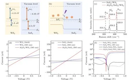
Fig.2.(a)–(b)The energy band alignment diagram of the SnS2/WS2 heterogeneous junction.(c)The Raman spectra of the SnS2/WS2 heterojunction(black line)and the sample with the Al2O3 capping layer(red line). (d)–(f)The I–V curves of the samples under dark(black lines)and 365 nm light illumination (blue and red lines) (d) for the WS2 (blue line) and Al2O3/WS2 (red line) samples, (e) for the SnS2 (blue line) and Al2O3/WS2 (red line)samples and(f)for the SnS2/WS2 heterogeneous junction with(red line)/without(blue line)the Al2O3 capping layer.

Based on theI–Vcharacteristics, the essential performance parameters related to the photodetectors are calculated. The photodetector based on the SnS2/WS2heterogeneous junction is hereinafter referred to as the control sample,while the photodetector with the Al2O3modified layer is hereinafter referred to as the Al2O3modified sample. The responsivity (R), normalized detectivity (D*), the noise equivalent power(NEP)of the photodetectors and external quantum efficiency(EQE)is calculated using the following formula:[50]whereIlightandIdarkare the photo-current and dark-current,respectively.Here,Pinis the effective power of the incident light,which is calculated by the total input power divided by the active area(A);andRImeans the responsivity at certain incident laser illumination(λ).The parameter Δfis defined as 1 in this work. As we know,the higher value ofR,D*,and EQE,while the NEP should be as low as possible, means better performance of the devices. The time-dependent photocurrent under 365 nm light irradiation with the bias voltage of 0 V was taken for the control sample and the Al2O3modified sample,as presented in Fig. 3(a). The photocurrent of both samples shows an increasing tendency with the higher input light power. The photocurrent and the incident laser power conform to the formulaIph∝Pθin,where the calculated value ofθis great than 1;thus,the responsivity shows an increasing trend with the light power, as shown in Fig. 3(b). It can be attributed to the fact that the light absorption in the heterogeneous junction region has not reached saturation,which can be attributed to the traps of the surface defect states that have captured a large number of photogenerated carriers. Therefore,the value of the responsivity increases with the increase in incident light power.From the curves presented in Fig.3(b),it can be concluded that the performance of the Al2O3modified sample was better than the control sample,and the performance of the photodetectors will be better with higher incident laser power. Figure 3(c)shows the relationship betweenD*and NEP of heterojunction-based devices with/without the Al2O3capping layer under different illumination power at 0 V bias voltage. It is observed that the device has low NEP, theD*can reach 3.36×10¹¹Jones and the EQE reaches 15.4 at 0 V bias voltage with 365 nm light radiation (11.10 nW) for the Al2O3modified sample in Figs.3(c)and 3(d). Therefore,it can be proved that the Al2O3modified WS2layer,SnS2layer and SnS2/WS2heterogeneous junction can reach more effective optical detection than that without the Al2O3modified layer. The better performance of the Al2O3modified sample is considered to be attributed to the passivation of the 2D materials’surface states and the tensile stress generated from the Al2O3layer.[12,46,47]The passivation of the surface states will enhance the transport of carriers because the surface states will induce charge scattering. Furthermore, as reported in our previous reports,[12,46,47]the Al2O3modified layers induce tensile stress leading to a higher electron concentration and smaller effective mass of electrons in the films. As a result,the conductivity of the layered materials will be increased and further enlarge the photocurrent.

Fig.3. The self-driven SnS2/WS2 van der Waals heterojunction photodetector with an Al2O3 layer and the control device under 365 nm illumination at zero bias voltage,for different input light power. (a)The time-dependent current under different incident power of the device with the Al2O3 layer(red line) and the control device without the Al2O3 layer (black line); (b) the responsivity (black lines) and photocurrent (red lines); (c) the NEP(black lines)and detectivity(red lines);and(d)the EQE of the Al2O3 layer device(red line)and the control(black line).

Table 1. Comparison of important performance parameters of the device in this work with other reported performance parameters of photodetectors based on 2D materials.

Fig.4. (a)The time-dependent photocurrent curves of the photodetector with(red line)/without (black line) Al2O3 for light power of 11.10 nW. (b)–(c)The single period of the time-dependent photocurrent curves of the control(black line)and with the Al2O3 layer(red line)samples with Pin=11.10 nW.
The time-dependent photocurrent property is an important indicator of photodetector performance. However, the photocurrent of the Al2O3modified sample shows a better linear relationship with the increase ofPinthan that of the control sample,which proves that the Al2O3modified sample is more sensitive to the change in input light power. Figure 4(a) exhibits the time-dependent photocurrent curves of the two samples under 365 nm light at the bias voltage of 0 V with thePinof 11.10 nW. The rise and decay time of the two samples are extracted in Figs. 4(b) and 4(c). It is found that the decay time of the two samples is similar but the rise time of the Al2O3modified sample is shorter than that of the control sample. The shorter rise time could be attributed to the fact that there are fewer surface states for the Al2O3modified sample. As a result, the photogenerated carrier will be transported as soon as possible without being trapped in the surface states. Further, the smaller effective mass of electrons in 2D materials caused by the tensile stress introduced by Al2O3is also beneficial for improving electron mobility. It is proved that a rapid response can be achieved with the Al2O3modified layer, which is suitable for improving the response time of photodetectors. Table 1 shows the comparisons of essential performance parameters of the heterojunction photodetectors in this work with some self-driven devices with similar structures. It can be seen that the performance of the detector with the Al2O3layer is improved more than the control device,which proves that the Al2O3layer can optimize the performance of the heterojunction detectors. The photo-responsivity of the SnS2/WS2heterojunction photodetector with the Al2O3layer demonstrated in this work is relatively higher than some of the reported results. Although our work has not achieved rapid response time and detectivity,it can provide a new idea for self-driven photodetectors with an oxide layer to further improve the performance.
4. Conclusion
A conductive band minimum matched self-driven SnS2/WS2-based van der Waals heterojunction photodetector with an Al2O3capping layer has been designed and fabricated in this work. Moreover, we systematically revealed the mechanics of energy band alignment at the interface of the SnS2/WS2heterostructure. However, in our previous reports,it has been proved that the Al2O3stress layer can be used to improve the performance of the photodetectors.As a result,by applying the Al2O3layer on the two-dimensional semiconductor materials,the performance of the self-driven photodetector has been increased. This is considered to be attributed to the Al2O3modified layers introducing tensile stress, leading to a higher electron concentration and smaller effective mass of electrons in the films. The fabricated heterostructure photodetector with the Al2O3modified layer shows better detection performance than that without Al2O3at a 0 V bias voltage with 365 nm light radiation. Moreover, the self-driven behaviour can be attributed to the fact that there is nearly no electronic barrier in the SnS2/WS2junction and the potential difference(ΔEc)in the heterogeneous junction can be effectively adjusted by applying the bias voltage on the substrate.
Acknowledgments
Project supported by the National Natural Science Foundation of China (Grant Nos. 61974144, 62004127, and 12074263),the Science and Technology Foundation of Shenzhen (Grant No. JSGG20191129114216474), and the “National”Taipei University of Technology–Shenzhen University Joint Research Program,China(Grant No.2020009).
猜你喜欢
杂志排行

Chinese Physics B的其它文章
- LAMOST medium-resolution spectroscopic survey of binarity and exotic star(LAMOST-MRS-B):Observation strategy and target selection
- Vertex centrality of complex networks based on joint nonnegative matrix factorization and graph embedding
- A novel lattice model integrating the cooperative deviation of density and optimal flux under V2X environment
- Effect of a static pedestrian as an exit obstacle on evacuation
- Chiral lateral optical force near plasmonic ring induced by Laguerre–Gaussian beam
- Adsorption dynamics of double-stranded DNA on a graphene oxide surface with both large unoxidized and oxidized regions