Method of measuring one-dimensional photonic crystal period-structure-film thickness based on Bloch surface wave enhanced Goos–H¨anchen shift
2023-02-20YaoPuLang郎垚璞QingGangLiu刘庆纲QiWang王奇XingLinZhou周兴林andGuangYiJia贾光一
Yao-Pu Lang(郎垚璞), Qing-Gang Liu(刘庆纲),†, Qi Wang(王奇),Xing-Lin Zhou(周兴林), and Guang-Yi Jia(贾光一)
1State Key Laboratory of Precision Measurement Technology and Instruments,Tianjin University,Tianjin 300072,China
2School of Communications,Wuhan University of Science and Technology,Wuhan 430081,China
3School of Science,Tianjin University of Commerce,Tianjin 300134,China
Keywords: thin film thickness,Bloch surface wave(BSW),Goos–H¨anchen shift,photonic crystal
1. Introduction
The photonic crystal film, composed of periodic combinations of materials with different dielectric constants or magnetic permeabilities,[1]has developed rapidly in recent years.It is widely used in optical devices, such as the high precision chemical and biosensors,[2–8]the optical filters,[9,10]the optical switch,[11]the optical color modulation,[12]the optical absorbers,[13,14]and the optical resonators,[15]as it can improve the reflectance of electromagnetic waves in a specific wavelength band,[16]and reduce the light propagation loss.The properties of photonic crystals are mainly dependent on their periodic structure forms and their material refractive indices. For one-dimensional photonic crystal(1DPC),the film thickness, including the thickness of periodic bilayer, has a great influence on the properties of the film. For example,the forbidden bandgap of the structure and the surface resonance modes excited,are modulated by the thickness of the photonic crystal material periodically aligned as well as the termination layer. Currently,the thickness parameters of 1DPC utilized by most of the researchers are also limited to the designed thickness of the periodical bilayer and the termination layer,rather than the actual measurement values of 1DPC.It is found that there are few reports on the methods of measuring the thickness of each layer of the photonic crystal film. Most of the photonic crystal films are processed and then calibrated for parameters prior to being used, rather than reaching the predesigned parameters. Therefore, the method to measure the thickness of 1DPC film is required in order to accurately character the properties of the photonic crystal film.
Bloch surface waves(BSWs)are electromagnetic surface waves existing at the interface between a homogeneous dielectric medium and an abruptly terminated photonic crystal,typically a periodic dielectric multilayer.[17]The BSW has its unique advantages,for example,it can be excited by TM or TE waves.The BSW does not require the precious metal coupling layer adopted by surface plasmon resonance(SPR),and has a wider range of material selectivity. The following problems are avoided: the damping and resonant broadening effects of the absorption of incident light by metal layer, the parameter adjustment inconvenience,[18]due to the relative fixation of the conditions suitable for stimulating the SPR effect.
The Goos–H¨anchen (GH) shift is a well-known optical phenomenon in which a light beam undergoes a small transverse displacement when it reaches an interface that satisfies the total internal reflection (TIR) condition.[19]This lateral displacement is proportional to the abrupt phase variation of the angular-dependent reflectance.[20]The GH effect can be enhanced by surface waves at the reflection interface[21–25]or the quasi-bound states in the continuum,[26]and many reports have demonstrated that GH shift can be enhanced to tens or even hundreds of times the wavelength by coupling the BSW[27]due to the electromagnetic surface waves excited at the interface between a homogeneous dielectric medium and an abruptly terminated photonic crystal. Many studies have demonstrated that the GH shift is closely related to the partial derivative of the reflection phase with respect to the incident light angle when the GH shift is investigated by the stationaryphase approach.[20,28–31]The GH shift can reach its maximum when the rate of phase variation is maximum. Because GH shift detection is the measurement of relative position, it is not affected by optical common-mode noise and has a higher signal-to-noise ratio than optical intensity detection.However,there is no report on the crystal period and termination layer thickness analysis by using an enhanced GH shift coupled with BSW.
Based on the above considerations,a characterization and measurement method for 1DPC film thickness by the GH shift coupled with BSW is proposed. The variations of the light reflectance and the GH shift of the 1DPC composed of TiO2and SiO2layers are investigated by the transmission matrix method. The effects of the angle of incidence,medium dispersion and surface roughness are taken into account,also.
2. Principle of Goos–H¨anchen shift enhanced by Bloch surface wave
The 1DPC consists of two dielectric layers with different dielectric constants as shown in Fig.1. When the high refractive index material A and low refractive index material B are arranged in a periodic alternating pattern,the 1DPC film possesses a photonic bandgap, which prevents light from propagating in certain directions at specified frequencies.[1]The reflectance of the light with the wavelength in the bandgap increases dramatically. The film thickness and the dispersion of the material are the most important factors in determining the photonic bandgap of a 1DPC,[32]and the desired photonic bandgap as well as its width can be obtained by designing its structure appropriately. The BSW is a localized mode that appears at the interface between a 1D photonic crystal and a dielectric. When the periodic structure of the photonic crystal is broken, the surface mode is greatly enhanced,[33]and the transmission loss is small. In this paper, the Krestchmann–Rather configuration is adopted to excite the BSW as shown in Fig. 1. The dielectric constant of the covering layer isε0and the dielectric constant of the prism isεS. The dielectric constant of the layer A and the termination layer A′are bothεA,and the dielectric constant of the layer B isεB. The corresponding values of thickness are denoted asdA,dA′, anddB,respectively.

Fig.1. Scheme of 1DPC Krestchmann–Rather configuration.
The characteristic matrix of single-layer film is expressed as

wherejis the subscript and denotes the layer A,B or A′,where the phase shiftδjis obtained from

withλbeing the wavelength of the incident light in the vacuum,njthe refractive index of the film,djthe physical thickness,θjthe refractive angle between the wave vector of the light in this layer and the normal of the film interface,andηjthe optical admittance. When the light of incidence is transverse electric (TE) wave, the optical admittance is expressed as

While for the transverse magnetic(TM)wave,the optical admittance is given by

whereϒ0is the optical admittance in vacuum. Then, the total characteristic matrixMTof theN-periodic photonic crystal can be obtained by concatenating the characteristic matrices of the single-layer film as follows:

The reflection coefficientrand the phaseφof the reflected light are given by

By using Eqs.(6)and(7),the reflection properties of thin film of 1DPC with different materials and structures under different light of incidence can be studied.
The GH shift expressed in Eq. (8)[30]is well suitable for the beams with a reflection angle greater than the critical angle. It must be emphasized that the equation is applicable only for the incident wave that is a plane wave or well collimated and the beam waist is wide enough.[29,34]In recent studies,equation(8)can be applied to all incident angles when the reflection occurs at the absorbing surface.[29]The 1DPC combined with special materials such as indium antimonide(InSb)[35]or the graphene-based hyperbolic metamaterial(GHMM),[36]will possess a GH shift around 182 times the wavelength.The BSW can also be used to enhance the GH shift.[20,25,34,37]When they are combined,the much larger GH shift which increases up to 2520 times the wavelength can be achieved.[37]

3. Calculation results and discussion
3.1. Feasibility of measuring film thickness via Goos–H¨anchen shift coupled with Bloch surface wave
The substrate material is BK7 glass. The 1DPC consists of TiO2as material A and SiO2as material B.The thicknesses of materials A and B are denoted asdAanddB, respectively.The material of terminating layer is TiO2and its thickness isdA′, and its covering layer is air. The incident light is in the TE mode. Owing to the importance of refractive index in the thickness solution, it should be determined first. The TiO2and SiO2nanoscale layers are deposited on silicon substrates by using the ion assistance electronic beam deposition technique and measured by ellipsometry. The refractive index dispersions of the constituent materials in a wavelength range of 210 nm–1200 nm are shown in Fig. 2(a), and the extinction coefficients are displayed in Fig. 2(b). The optical constants of SiO2are fitted by the Cauchy model,[38]those of BK7 glasses are fitted by the Cody–Lorentz model,[38,39]and those of TiO2by using the Tauc–Lorentz model.[38,40]The details of the models and values of the fitting parameters are given in Appendix A.
To match the energy loss due to the roughness of the thin film,the extinction coefficient of TiO2is set to be 10-3in the visible light range.[27]Based on the same consideration, the extinction coefficient of SiO2is assumed to be 1×10⁶.
When the 1DPC film withdA= 144.1 nm anddB=161 nm is considered as a semi-infinite (N=300, the number of periodic layers)film, figure 3 shows the bandgaps(for TE mode) of the structure clearly. The deep red area shows a low reflectance area, and the incident light in this area is allowed to pass through this film. The yellow area shows a high reflectance area. In this area,the incident light is forbidden to pass through this film,e.g.the bandgap. And then,the structure is simulated as a finite (N=3) and interrupted periodic structure by a layer of TiO2(dA′=41.5 nm), and the reflectance is shown in Fig.4(a)while the incident light is in the TE mode. The deep red curve, in a wavelength range of 612 nm–939 nm,shows a deep reflectance dip which is caused by the excited BSW in the bandgap. Several reflectance decay phenomena can be seen in Fig.4(a)(at smaller wavelengths),which are caused by the bandgap edge of the photonic crystal. The depths of these changes are less than the reflectance minimum values associated with the excitation of a BSW.The research is therefore focused on BSW.

Fig.2. Curves of (a) refractive index and (b) extinction coefficient versus wavelength of constituent materials.

Fig.3. Reflectance of 1DPC(dA=144.1 nm,dB=161 nm)under approximate semi-infinite conditions for TE mode, with deep red region regarded the photonic bandgap.
Figure 4(b)shows the spectral reflectance when the angle of incidence is 70.5°,the lowest reflectance at a wavelength of 676.1 nm is 0.01. In order to show the variation of reflectance,phase and GH shift more clearly,the axes are restricted to 68°–73°and 650 nn–700 nm in Figs.5–7.

Fig.4.(a)Reflectance of finite 1DPC(dA=144.1 nm,dB=161 nm,N=3,dA′ =41.5 nm)and(b)spectral reflectance versus wavelength at θ0=70.5°for TE mode.

Fig.5. Reflectance versus incident angle and wavelength for TE mode of finite 1DPC with dA=144.1 nm,dB=161 nm,N=3,and dA′ =41.5 nm.
To show the condition of the GH shift peak position more clearly,the reflectance of the region,where the peak GH shift is located(wavelength from 650 nm to 700 nm,incidence angle from 68°to 73°), is intercepted as shown in Fig. 5. The phase of the reflected light,shown in Fig.6,also changes dramatically with the reflectance decreasing sharply. Since the sampling interval is 0.05 nm,the lower right part of the curve in Fig.6 is serrated. If the sampling interval is small enough(less than 0.0001 nm or 0.0001°, the curve will become smoothly. It is unnecessary to display such a smooth curve here because the actual system cannot take so fine sampling interval.The position with the lowest reflectance is not the position with the largest phase change, but the position has the largest phase change rate. The GH shift is proportional to the angle-dependent phase variation when experiments are performed with a single wavelength light source.[20,28–31]When the wavelength is modified,the derivative of the phase with respect to the incident angle varies consequently. Thus, a large GH shift can also be generated by changing the wavelength.

Fig.6. Phase versus incident angle and wavelength of reflected light for TE mode of finite 1DPC, with dA =144.1 nm, dB =161 nm, N =3,and dA′ =41.5 nm.

Fig.7. GH shift versus incident angle and wavelength for TE mode of finite 1DPC, with dA = 144.1 nm, dB = 161 nm, N = 3, and dA′=41.5 nm,and deep red point at the intersection of the white dashed lines indicating the largest GH shift.
Although a few of obvious phase variations can be seen in Fig. 7 when the wavelength is above 685 nm, there are no GH shifts with larger values than that at an incident angle of 70.5°and a wavelength of 676.1 nm,as the rate of phase variation is the most decisive factor.It should be additionally stated that the accumulated phase change will goes beyond the range from-πtoπ. In order to calculate the rate of phase change,the phase is expressed not only as the phase in one period,but also as the cumulative change of the phase from the beginning to the present, to avoid the calculation error of the GH shift caused by subtracting 2π.
It can be found that the huge GH shift peaks, which are shown in Fig. 7 and distributed along the curve of the abrupt reflectance change as indicated in Fig.5,seem to be distributed discretely. This is because only the specific combination of incident angle and wavelength can excite large GH shift,and the calculations are performed by interval sampling to obtain theoretically continuous angular and wavelength variations,therefore,these GH shift peaks appear to be discretely distributed.Whenθ0= 70.5°andλ= 676.1 nm, the largest GH shift,3.46×106nm, about 5120 times the wavelength, will occur as shown by the dark red point in Fig. 7. Based on this discrete distribution, it can be more easily to discern the change in thickness of the 1DPC film.
3.2. Peak shift and peak wavelength of Goos–H¨anchen shift versus layer thickness
As shown in Fig.8,when the thickness of the termination layer(i.e.,dA′)varies from 41.1 nm to 41.5 nm(θ0=70.5°),the value of GH shift peak increases from 2×10⁶nm to about 5×10⁶nm and the wavelength position where the peak is located (called peak wavelength), shifts from 673.4 nm to 676.1 nm. For every 0.1-nm change in termination thickness,the peak wavelength varies approximately linearly by 0.7 nm.This resolution is sufficient to distinguish thickness changes of at least 0.1 nm.
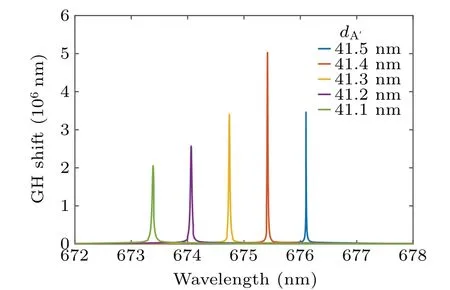
Fig.8. Simulated GH shift for TE mode with dA′ from 41.1 nm to 41.5 nm.

Fig.10. Simulation for TE mode with dA =71.3 nm, dB =172.9 nm. (a) reflectance, semi-infinite (N =300); (b) reflectance, N =6,dA′ =42.0 nm;(c)phase,N=6,dA′ =42.0 nm;(d)GH shift,N=6,dA′ =42.0 nm.
Like the termination layer, when the thickness values of the periodic bilayers (dAanddB) change, the GH shift peak and the peak wavelength also change as shown in Fig. 9.The resolution of the periodic bilayers obtained from the peak wavelength is slightly lower than that of the thickness of the termination layer. The resolution obtained from the GH shift peaks can provide enough support for obtaining the solution ofdAanddB.

Fig.9.Plots of simulated GH shift versus wavelength for TE mode with thickness(a)dA from 144.1 nm to 144.5 nm and(b)dB from 160.6 nm to 161.0 nm.
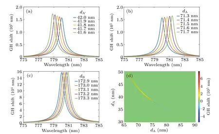
Fig.11. Simulated GH shift for TE mode with different thickness values: (a) dA′ from 41.6 nm to 42 nm, (b) dA from 71.3 nm to 71.7 nm,(c)dB from 172.9 nm to 173.3 nm,and(d)dA′ from 30 nm to 50 nm and dA from 65 nm to 90 nm.
Similar conclusions can be obtained when a different 1DPC structure,e.g.,dA=71.3 nm anddB=172.9 nm, is simulated. If this structure is considered to be semi-infinite,the reflectance is shown in Fig.10(a). If a more realistic finite structure(N=6 anddA′ =42.0 nm)is simulated as shown in Fig. 10(b), reflectance dips due to BSW can be found in the photonic bandgap. Both the phase and the GH shift also have huge changes because of BSW as shown in Figs. 10(c) and 10(d). Similarly,when the thickness values of the termination layer and the periodic bilayer vary at an interval of 0.1 nm,the value of the GH shift peak and the peak wavelength also change significantly. As shown in Figs. 11(a)–11(c), these peak wavelengths change almost linearly, too. These results prove that the detection of thickness by the enhanced GH shift is not only useful for the special structure (dA=144.1 nm,dB=161 nm,N=3,dA′ =41.5 nm),but also widely applicable.
3.3. Method of determining layer thickness
When bothdAanddA′are uncertain (θ0=49.9 nm andλ=779.2 nm),the GH shifts,shown in Fig.11(d),can be obtained. It can be clearly seen that with some thickness combinations,there are obvious GH shift peaks. But it is not enough to solve the thickness of a particular layer alone. The feasible solution is to obtain more such GH shift distribution maps bychanging the wavelength and the angle of incidence to determine the unique thickness combination. As shown in Fig.12,there are differences in the distributions of GH shifts among different films at different wavelengths,especially in the case of excited BSW. These differences allow us to calculate the thickness values of the films. It can be expected that the accuracies of such calculations will further be improved if the angular dimension is taken into consideration.
According to the simulation results, it is clear that both the periodic bilayers and the thickness of the termination layer have a decisive influence on the GH shift. When calculating the film thickness, the thickness of the termination layer cannot be calculated without obtaining the thickness of the bilayer periodic structure.Therefore,the optimization algorithm from machine learning technique is needed to perform the solution of the overall 1DPC structure by sampling at different incident light and wavelengths.

Fig.12. GH shift versus dA,dA′,and wavelength in TE mode.
In this work,according to the target thickness in processing, the limitations for the true thickness of the termination layer and the periodic bilayer are preset. The particle swarm optimization (PSO) is initialized to give a group of random particles(random solutions),and then to find the solution that best meets the requirements for iteration,i.e., the optimal solution under a specific evaluation function. In each iteration,the particles gradually converge toward the optimal solution by tracking the better solution. In addition, the trapping into local optimum is avoided by adding unexpected variables. A more accurate thickness combination can be obtained by increasing the weight of the peak GH shift as well as the peak wavelength in the evaluation function through the adjustment for the evaluation function. The accurate film thickness can be achieved when the thickness range of the termination layers and the periodic bilayer are limited to±10 nm and±50 nm of the target thickness respectively.
A more general film, withdA= 126.9 nm,dB=236.1 nm,N= 5, anddA′= 87.2 nm is chosen as the object of thickness distribution solution. It is difficult to achieve sub-nanometer accuracy when actually manufacturing the film(therefore the film is not always a perfect periodic in structure),so calculation results are retained to two decimal places to support the process. The GH shift obtained from the simulation is used as the‘measured value’for the evaluation of the solution method. As the solving results that are shown in Table 1, the repeatability error of the termination layer thickness measurement is less than 2% with an accuracy error ofσ=±2 nm,and the repeatability error of the periodic layer measurement is less than 3‰with an accuracy error ofσ=±0.5 nm. The first sample mentioned in this work (e.g.,dA= 144.1 nm,dB=161 nm,N=3, anddA′=41.5 nm) is also used as the subject for calculation and the results are shown in Table 2.

Table 1. Solving result for dA=126.9 nm,dB=236.1 nm,N=5,and dA′ =87.2 nm.

Table 2. Solving result for dA =144.1 nm, dB =161 nm, N =3, and dA′ =41.5 nm.
As this sample induces a more intensive BSW, the repeatability error of the termination layer thickness measurement is less than 5‰with an accuracy error ofσ=±0.5 nm,and the repeatability error of the periodic layer measurement is less than 5‰with an accuracy error ofσ=±2 nm. It shows that when the BSW is more intensive, the results are better for the termination layer,while the accuracy of the calculation will decrease for the periodic structure.
4. Conclusions
The models of 1DPC with different structures are studied by the transmission matrix method in the work. The reflectance, reflection phase, and the distribution of GH shifts are given for different incidence conditions. It is demonstrated that large GH shifts of the order of 5.1×10³times the wavelength can occur under specific conditions (e.g.,dA=144.1 nm,dB=161 nm,N=3, anddA′=41.5 nm). When multiple thickness values of the layers are varied,the peak position of the GH shifts and the peak wavelength changes accordingly. And another structure with a GH shift of 30 times the wavelength magnitude is chosen as the object of thickness distribution solution. The changes occurring are sufficient to carry out the resolution of the thickness. Therefore,after multi-wavelength sampling,the thickness of the termination layer and the periodic bilayer can be solved by GH shifts combined with the PSO algorithm. As 1DPC-based sensors and optical fibers are more and more widely used in the field of optical communication and sensing, this BSW enhanced GH shift provides an innovative idea of analyzation and calibration for 1DPC film, and can provide the guidance for on-line application of multilayer film.
Appendix A:Material model and fitting parameters
In this section the models of the optical constants of the materials are briefly presented, please see Fig. 2 in the main body for the exact values. These values are calculated from the internal analysis of the Ellipsometer. In all three models,theEis light quantum energy. The Cauchy model[38]for the optical constant of SiO2is given by

whereλis the wavelength in unit of μm,A,B,C, and kamp are the their fitting parameters,bandedge is the parameter that can be set manually,[38]specifically,A=1.479,B=0.00411,C=0,kamp=0,and bandedge=4 eV.
The Tauc–Lorentz model[38,40]for the dielectric constant of TiO2is given by

where
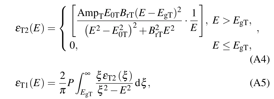
wherePis the Cauchy principal part of the integral; AmpT,BrT,EoT, andEgTare the variable fitting parameters, specifically,AmpT=258.5002,BrT=2.035,ET=4.123,andEgT=3.295.
The Cody–Lorentz model[38,39]for the dielectric constant of BK7 is given by


where

TheAB,ΓB,EB,EgB,EpB,EtB, andEuBare variable fitting parameters. In this paper,AB= 0.00130,ΓB= 0.454,EB= 4.492,EgB= 3.035,EpB= 8.339,EtB= 0.000, andEuB= 0.500. The refractive indices and extinction coefficients of TiO2can be calculated fromεT1=n2TiO2-k2TiO2andεT2= 2nTiO2kTiO2. For BK7,εB1=n2BK7-k2BK7andεB2=2nBK7kBK7.
Acknowledgements
The authors thank Dr.Zirui Qin and Dr.Chong Yue,graduated from our group,for their valuable discussion in the modeling process, and also thank Prof. Dr. Reza Asgari, School of Physics, Institute for Research in Fundamental Sciences,(IPM) 19395-5531 Tehran, Iran, for the discussion and suggestion of related issues.
Project supported by the National Natural Science Foundation of China(Grant Nos.51575387 and 51827812).
猜你喜欢
杂志排行
Chinese Physics B的其它文章
- LAMOST medium-resolution spectroscopic survey of binarity and exotic star(LAMOST-MRS-B):Observation strategy and target selection
- Vertex centrality of complex networks based on joint nonnegative matrix factorization and graph embedding
- A novel lattice model integrating the cooperative deviation of density and optimal flux under V2X environment
- Effect of a static pedestrian as an exit obstacle on evacuation
- Chiral lateral optical force near plasmonic ring induced by Laguerre–Gaussian beam
- Adsorption dynamics of double-stranded DNA on a graphene oxide surface with both large unoxidized and oxidized regions