High frequency doubling efficiency THz GaAs Schottky barrier diode based on inverted trapezoidal epitaxial cross-section structure
2023-02-20XiaoyuLiu刘晓宇YongZhang张勇HaoranWang王皓冉HaomiaoWei魏浩淼JingtaoZhou周静涛ZhiJin金智YuehangXu徐跃杭andBoYan延波
Xiaoyu Liu(刘晓宇), Yong Zhang(张勇), Haoran Wang(王皓冉), Haomiao Wei(魏浩淼),Jingtao Zhou(周静涛),‡, Zhi Jin(金智), Yuehang Xu(徐跃杭), and Bo Yan(延波)
1University of Electronic Science and Technology of China,Chengdu 611731,China
2Institute of Microelectronics of the Chinese Academy of Sciences,Beijing 100029,China
Keywords: inverted trapezoidal epitaxial cross-section structure, doubler, Schottky barrier diode (SBD),GaAs,terahertz,capacitance modulation ratio
1. Introduction
Increasing demand for terahertz (THz) devices has been generated due to the development of THz applications, such as communication, biology, and sensing applications.[1–3]The development of the THz spectrum faces with many technical challenges, including generation, detection, and modulation.[4,5]Obtaining a high-performance THz source is an important direction of the THz technology research.[1]One suitable way to generate a THz wave is by THz solid-state source multiplying the millimeter wave, which is realized by frequency multipliers.[6–9]Schottky barrier diode (SBD) is a suitable device for the advantages of low parasitic effect,high cut-off frequency, and the ability to work at the room temperature.[10,11]GaAs SBD is the most widely used SBD of high output power multipliers due to their large electron mobility, high withstand voltage characteristics, and uniform epitaxial material quality.[12,13]
The SBD in the frequency multipliers usually works in a negative bias state, and the generation of harmonics of the frequency multiplier is realized by the nonlinear displacement current. This nonlinear displacement current is realized by the nonlinear change of junction capacitance with the voltage of the Schottky contact. In recent research, it is found that the edge field effect on the Schottky metal–semiconductor interface results in a wider spreading depletion edge and a larger leakage current.[14–16]This phenomenon of spreading at the edge of the depletion layer affects the varactor characteristics of the diode,[15,17]which will induce the poor conversion efficiency of the multipliers. Termination structures such as the field plate[18,19]and the diffusion guard ring[20,21]can effectively correct the phenomenon of the depletion layer extension,but the parasitic capacitance introduced by them will further deteriorate the varactor characteristics of the diode.
In this paper, an inverted trapezoidal epitaxial crosssection SBD has been designed and fabricated. It exhibits a high grading coefficient of 0.52, compared with a normal structure of 0.47. The capacitance modulation ratio(Cmax/Cmin) also increases from 6.70 to 7.61. The frequency multiplication performance of this diode is verified by a 190 GHz frequency multiplier, and the frequency multiplication efficiency of the frequency multiplier is increased from 30%to 35%.
2. Simulation and fabrication
Figure 1(a) shows the basic structures of the inverted trapezoidal epitaxial cross-section SBD, and Fig. 1(b) shows the SEM image of the overall structure of the diode. Figure 1(c) depicts the Schottky diode metal and the underlying inverted trapezoidal epitaxial layer, and Fig. 1(d) shows the cross-sectional view of the inverted trapezoidal epitaxial cross-section structure. The epitaxial wafer is grown on a 2-inch GaAs semi-insulating substrate by metal–organic chemical vapor deposition (MOCVD), consisting of a 50 nm Al-GaAs etch stop layer,1.5 μm n+GaAs conducting layer(ND:5×1018cm-3), and 300 nm n- GaAs epitaxial layer (ND:2×1017cm-3).

Fig.1. (a)Schematic of the inverted trapezoidal epitaxial cross-section SBD.(b)SEM image of the inverted trapezoidal epitaxial cross-section SBD.(c)Schottky metal structure details. (d)Inverted trapezoidal epitaxial cross-section structure details.
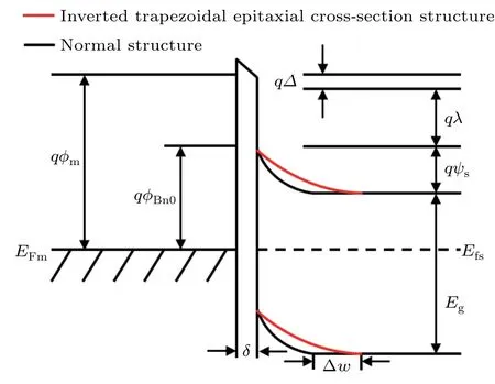
Fig.2. Energy band diagram of the MIS model. The red line represents the energy band of the inverted trapezoidal epitaxial cross-section structure,in which Δw increases with decreasing distance from the edge of the anode metal.
The electrical simulations of the metal–interface–semiconductor(MIS)model[22]which is described in this paper are performed using the Sentaurus TCAD tool.[23]The model is based on the basic drift–diffusion and Poisson equations for direct current (DC), breakdown characteristics, and small-signal simulation. This basic drift–diffusion model includes the Fermi statistics, mobility with doping dependence and high-velocity saturation model,carrier generation,recombination,non-local tunneling,and band to band tunneling.The drift–diffusion for electrons and Poisson equations are given respectively by

whereJnis the electron current density,qis the electron charge.μnis the mobility,nis the electron density,pis the hole density,kis the Boltzmann constant,Tis the temperature,mnis the effective electron mass,γnis the Boltzmann statistics,εis the electrical permittivity,φis the electrostatic potential,Pis the ferroelectric polarization,andNDandNAare the concentrations of ionized donors and acceptors,respectively.
In the simulation,the two-dimensional(2D)structures are depicted in Fig.1(a)and the doping levels are described above.The band diagram of the inverted trapezoidal epitaxial crosssection structure is shown in Fig. 2. The structure of the different inverted trapezoid angles and Schottky contact diameters are simulated to explore their influence on the varactor characteristics of the SBD.Furthermore,we conduct tape-out processing of the inverted trapezoidal epitaxial cross-sectional structure to verify the validity of this structure.
Figure 3 demonstrates a revised process for the inverted trapezoidal epitaxial cross-section SBD. Initially, a Ti/Pt/Au metal is deposited by e-beam evaporation as anode Schottky contacts with a lower ideal factor. The Ti is used to form an ohmic contact with the epitaxial layer, and the Pt is used to block the diffusion of Au atoms.The Ni/Ge/Au cathode ohmic metal is deposited on the wet etched n+ GaAs conducting layer. Further, an inverted trapezoidal epitaxial cross-section structure is formed by inductively coupled plasma (ICP) dry etching and H3PO4/H2O2/H2O wet etching aided by a certain power ultrasound. During ICP etching, BCl3, Cl2, and Ar are used as a primary etching gas for the PR-masked etching samples.[24]Later, samples are passivated with 200 nm SiO2,and the dielectric layer existing on top of the metal contacts is removed by CHF3based ICP dry etching. The detailed etching parameters of the above two materials are listed in Table 1. Subsequently, metal fingers and other connecting metals are formed with the Ti/Au metal system, and the mesas are formed by using an H3PO4/H2O2/H2O wet etching to achieve the production of the air bridge.The morphology of the inverted trapezoidal epitaxial cross-section SBD is shown in Figs.1(b)–1(d).

Table 1. Etching parameters of the PR-masked GaAs samples etching.
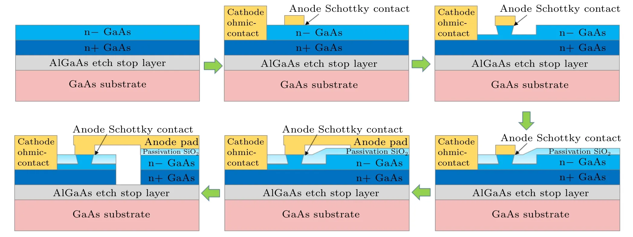
Fig.3. Process flow diagram of the inverted trapezoidal epitaxial cross-section SBD.
3. Result and discussion
According to the thermal electron emission model,[25]the current–voltage curve across the SBD can be described by

whereIsis the reverse saturated current,andnis the ideal factor.When the diode voltage is less than the barrier voltage,the diode has a linear relationship between current and voltage at a semi-log-scale.
Figure 4 shows the measured forwardI–Vcharacteristics and ideal factors of a series of different structures,which is dominated by the thermionic emission (TE) model, with a Schottky barrier height (Vb) of 0.67 eV extracted based on the Richardson plot.[26]The ideal factor is a figure of merit that describes an unnecessary current path except for the thermionic electron emission current,which is induced by interfacial disorder, interface state densities, and electron tunneling current.[27]It is shown in Fig.4 that the ideal factor of the Schottky junction with a diameter of 3 μm is less than 1.2.The inverted trapezoidal epitaxial cross-sectional structure is consistent with the normal diode forwardI–Vcharacteristics.
Figure 5 shows the measured reverseI–Vcharacteristics of different structures with a junction diameter of 3 μm. The GaAs SBD with different structures has the breakdown voltage of the order of-9.8 V for the inverted trapezoidal epitaxial cross-sectional structure and-9.1 V for the normal structure,respectively. The inverted trapezoidal epitaxial cross-section SBD shows the advantage of a high breakdown voltage due to reducing the path of tunneling current caused by the high electric field at the edges. The leakage current caused by electron tunneling is significantly lower than that of normal SBD.Simulated results based on the MIS model and the measurement results show a good agreement as shown in Fig. 4. The difference between the simulation and the measurement results of the inverted trapezoidal epitaxial cross-section structure in Fig.5 is mainly caused by different corrosion rates of a circular mesa in each direction during the wet etching process.
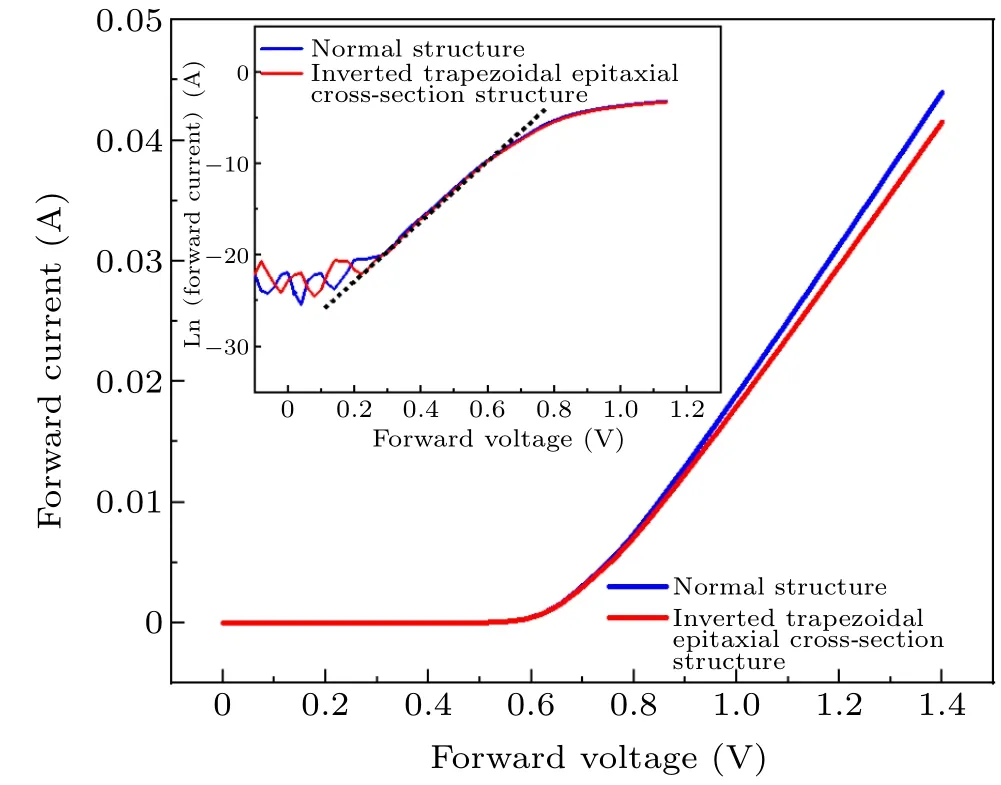
Fig.4.Forward I–V characteristics of the inverted trapezoidal epitaxial crosssection SBD and normal SBD with a diameter of 3 μm in linear-scale and semi-log-scale.
Figure 6 shows the measuredC–Vcharacteristics of different structures with a junction diameter of 3 μm. The extracted junction capacitances at zero bias(Cj0)of the inverted trapezoidal epitaxial cross-section structure are 11.8 fF and 12.4 fF for the normal structure, respectively. To better show the correction of the varactor characteristics of the diode by the inverted trapezoidal epitaxial cross-sectional structure,the reverseC–Vcharacteristics of diodes of different structures are displayed under the 1/C2scale. Combining with the open report of the interface state capacitance in Refs.[15,17],we can provide a simple analytical expression to describe the capacitive behavior of SBD,
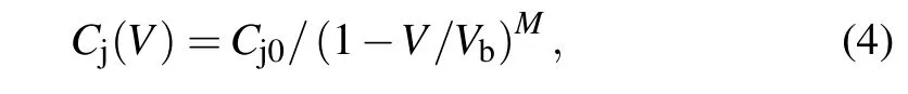
whereMis the grade coefficient and is ideally fixed at 0.5.The value ofMcan reflect the varactor performance of the diode within a certain range. The diode varactor ratio increases asMincreases. The normal SBD has a narrow spreading depletion layer near the edge of the anode electrode, which results in a reduction in the varactor ratio of the diode with theMof 0.47.The inverted trapezoidal epitaxial cross-section structure can effectively eliminate a spreading narrow depletion layer near the edge of the anode electrode caused by the accumulation of electrons. The inverted trapezoidal epitaxial cross-section SBD demonstrates a better variable capacitance characteristic with theMof 0.52. Furthermore,we use the capacitance modulation ratio (Cmax/Cmin) to characterize the varactor characteristics of different diode structures,whereCmaxandCminare the junction capacitance at a bias voltage of 0.5 V and-5 V.The capacitance modulation ratio for the inverted trapezoidal epitaxial cross-section structure and the normal structure with a junction diameter of 3 μm are 7.61 and 6.70,respectively.
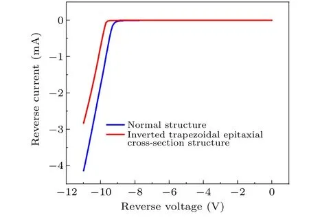
Fig.5.Reverse I–V characteristics of the inverted trapezoidal epitaxial crosssection SBD and the normal SBD with a diameter of 3 μm in linear scale.
The effect of this optimized varactor characteristic is more obvious in SBDs with small Schottky junction diameters. In order to investigate the physical mechanism of SBDs with small Schottky junction diameters,electrical simulations are carried out to precisely extract the capacitance characteristics at different reverse bias voltages and distribution of electric field and space charge. Figure 7 shows the simulationC–Vcharacteristics of different structures with a junction diameter of 1 μm. TheCj0of the inverted trapezoidal epitaxial cross-section structure and the normal structures are 1.31 fF and 1.47 fF withMof 0.54 and 0.44,respectively. The capacitance modulation ratio for the inverted trapezoidal epitaxial cross-section structure and the normal structure are 7.61 and 5.49.
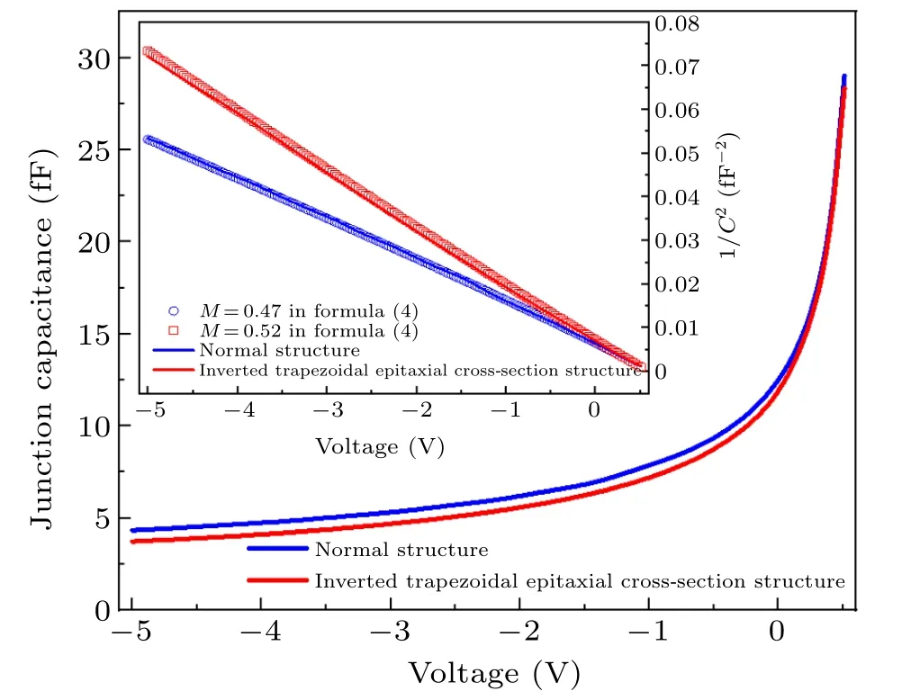
Fig.6.The C–V characteristics of inverted trapezoidal epitaxial cross-section SBD and normal SBD with a diameter of 3 μm in linear-scale and 1/C2-scale.
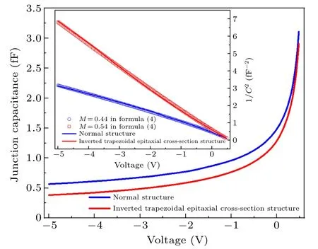
Fig.7.The C–V characteristics of inverted trapezoidal epitaxial cross-section SBD and normal SBD with a diameter of 1 μm in linear-scale and 1/C2-scale.
It can be seen in Fig. 8 that the inverted trapezoidal epitaxial cross-section structure eliminates the spreading narrow depletion layer. The electrons that originally packed around the anode in the normal structure are squeezed down along the edge of the etched epitaxial layer, which changes the shape of the depletion layer. This change not only eliminates the high electric field region at the edge of the anode but also constrains the depletion layer to change only in the vertical direction, thereby improving the varactor characteristics of the junction capacitance. This phenomenon is more pronounced in small Schottky junction size SBDs.
We also simulate a 190 GHz frequency doubler with a 3D full-wave simulation software high-frequency structure simulator (HFSS) and circuit simulation software advanced design systems (ADS) to verify the inverted trapezoidal epitaxial cross-section structure at the application level, as shown in Fig. 9. Figure 10 shows the simulation results that in the saturation power range the inverted trapezoidal epitaxial cross-section structure has a higher frequency doubling the efficiency of 35% compared to that of the normal structure of 30%,which contributes to its better varactor characteristics.
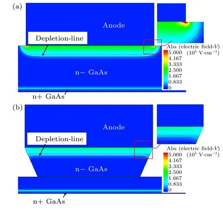
Fig.8.Depletion layer area(white line)and electric field distribution near the edge of the anode metal of(a)normal SBD.(b)Inverted trapezoidal epitaxial cross-section SBD.
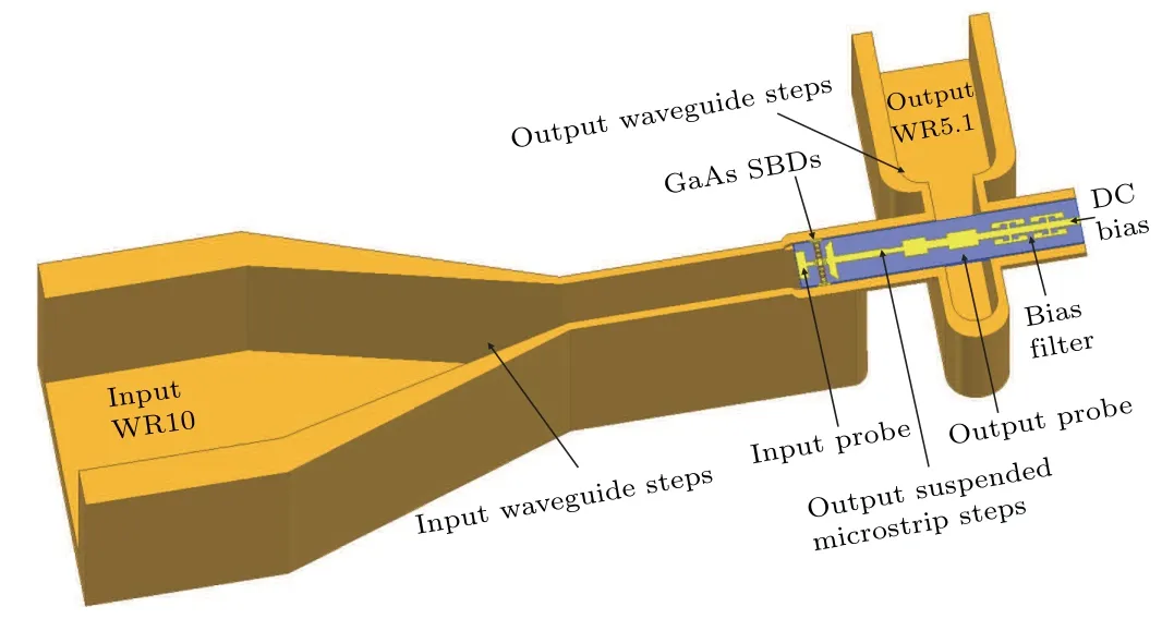
Fig.9. The configuration of the 170 GHz–200 GHz balanced frequency doubler.
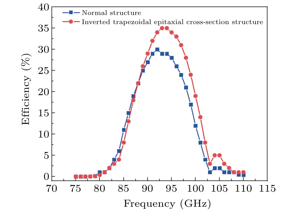
Fig.10. Simulation results of the doubling efficiency of the 190 GHz frequency doubler based on two diode structures.
4. Conclusion
This paper reports a new type of diode structure with an inverted trapezoidal epitaxial cross-section structure. The inverted trapezoidal cross-sectional profile of the epitaxial layer is achieved by ICP dry etching and dissolution wet etching.Compared to that of the normal structure, the grading coefficientMincreases from 0.47 to 0.52, and the capacitance modulation ratio (Cmax/Cmin) increases from 6.70 to 7.61.The inverted trapezoidal epitaxial cross-sectional structure is a promising approach to improve the variable-capacity ratio by eliminating the accumulation of charge at the Schottky electrode edge. A 190 GHz frequency doubler based on the inverted trapezoidal epitaxial cross-section SBD also shows a doubling efficiency of 35% compared to that of the normal SBD of 30%. There is a good prospect in the future that the THz frequency multiplier applies to the inverted trapezoidal epitaxial cross-section SBD.
Acknowledgment
Project supported by the National Natural Science Foundation of China(Grant No.61871072).
猜你喜欢
杂志排行

Chinese Physics B的其它文章
- LAMOST medium-resolution spectroscopic survey of binarity and exotic star(LAMOST-MRS-B):Observation strategy and target selection
- Vertex centrality of complex networks based on joint nonnegative matrix factorization and graph embedding
- A novel lattice model integrating the cooperative deviation of density and optimal flux under V2X environment
- Effect of a static pedestrian as an exit obstacle on evacuation
- Chiral lateral optical force near plasmonic ring induced by Laguerre–Gaussian beam
- Adsorption dynamics of double-stranded DNA on a graphene oxide surface with both large unoxidized and oxidized regions