Measurement and Characterization of Microwave Interaction between Integrated Distributed Feedback Laser Diode and EIectro-Absorption ModuIator
2023-01-13FeiYuanChaoJingMengKeWangShangJianZhangZhiYaoZhangYongLiu
Fei Yuan | Chao Jing | Meng-Ke Wang | Shang-Jian Zhang | Zhi-Yao Zhang | Yong Liu
Abstract—Integrated electro-absorption-modulated distributed feedback laser diodes (EMLs) are attracting much interest in optical communications for the advantages of a compact structure,low power consumption,and highspeed modulation.In integrated EML,the microwave interaction between the distributed feedback laser diode(DFB-LD) and the electro-absorption modulator (EAM) has a nonnegligible influence on the modulation performance,especially at the high-frequency region.In this paper,integrated EML was investigated as a three-port network with two electrical inputs and a single optical output,where the scattering matrix of the integrated device was theoretically deduced and experimentally measured.Based on the theoretical model and the measured data,the microwave equivalent circuit model of the integrated device was established,from which the microwave interaction between DFB-LD and EAM was successfully extracted.The results reveal that the microwave interaction within integrated EML contains both the electrical isolation and optical coupling.The electrical isolation is bidirectional while the optical coupling is directional,which aggravates the microwave interaction in the direction from DFB-LD to EAM.
1.Introduction
High-density and cost-effective photonic integration circuits (PICs) are considered as promising candidates for future high-performance computers and datacenters[1],[2].Integrated electro-absorptionmodulated distributed feedback laser diodes (EMLs) are regarded as reliable optical sources in these applications,since they have many advantages,such as a compact structure,low power consumption,and the high-speed modulation capability[3],[4].In the past decades,most active photonic components were fabricated on the III-V monolithic integration platform[3].Recently,silicon photon integration technologies have been demonstrated with scalability up to a large substrate (up to 450 mm today) and compatibility with complementary metal oxide semiconductor (CMOS) fabrication[5].In particular,the heterogeneous III-V silicon integration allows solutions for chip-level distributed feedback laser diodes (DFB-LDs),electro-absorption modulators (EAMs),and positive-intrinsic-negative (PIN) photodiodes by integrating different III-V materials onto a single silicon substrate,which enables versatile functional components on one wafer for varied applications[6]-[8].
In integrated EML,the proper isolation between forward-bias DFB-LD and reverse-bias EAM is indispensable[4],[9],[10].The low electrical isolation will result in the increase of the threshold current and the decrease of the output power,and the variation of the optical reflection and coupling will influence the lasing properties[9]-[11].In addition,a small isolation resistance may cause relatively large unwanted additional modulation of DFB-LD at the high-frequency regime[11]-[13].Therefore,a comprehensive model to characterize integrated EML is favorable for designing high-performance integrated EML.
In this paper,a model to characterize integrated EML was proposed and experimentally demonstrated.Integrated EML was investigated as an electrical-electrical-optical integrated device with two electrical input ports and a single optical output port,and was characterized in terms of the electrical-to-optical and electricalto-electrical scattering matrices between DFB-LD and EAM.Based on the proposed theoretical model and the measured data,the high-frequency equivalent circuit model of integrated EML was established,which can be used to accurately extract the microwave interaction between DFB-LD and EAM.
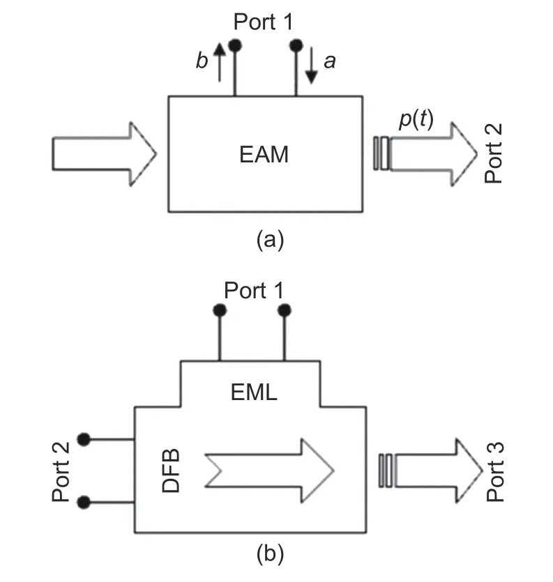
Fig.1.Schematic diagrams of (a) EAM and (b) integrated EML.
2.Methods
Figs.1 (a) and (b) show the schematic diagrams of EAM and integrated EML,respectively.From the view of modulation,there are two ports for EAM,including an electrical input port and an optical output port.For integrated EML,there are three ports,i.e.,two electrical input ports and a single optical output port.
As shown in Fig.1 (a),EAM uses electrical signals at its input port (Port 1) to linearly modulate the intensity (power) of the input light wave.The instantaneous output optical power at the optical port (Port 2)can be written as[14]

wherep0is the average optical power,mis the modulation index,αis the phase of the modulation envelope,ωis the angular frequency of the microwave signal,andtis the time of modulation.In terms of the optical powerp(t) at the optical port,and the incident waveaand the reflected wavebat the electrical port,the scattering matrix of EAM can be expressed as[14]

where the subscripts 1 and 2 denote the electrical and optical ports,respectively.
In integrated EML,DFB-LD is generally biased at the forward current and kept in continuous-wave operation,and EAM is biased at the reverse voltage and modulated by a high-frequency microwave signal.In addition,the integrated device can also be operated under direct modulation at the DFB-LD part.Therefore,integrated EML can be considered as an electrical-electrical-optical three-port network with two electrical input ports and a single optical output port,as shown in Fig.1 (b).Similar to the aforementioned deduction,integrated EML can be described by a scattering matrix as

whereS11andS31are mainly from the reflection coefficient and the modulation response of EAM,respectively;similarly,S22andS32are from DFB-LD;S12andS21denote the transmission coefficients of the two electrical ports,which represent the microwave interaction between DFB-LD and EAM.
3.Experiment Description
Fig.2 shows an integrated EML chip under test,which is mounted on an AlN submount with three coplanar electrodes.One of the electrodes is directly connected with the bottom-contact of the integrated chip,and the other two are connected to the top signal electrodes of DFB-LD and EAM by bonding wires.The coplanar electrodes of the EAM part are paralleled with a 50-Ω thin film resistor for impedance match.
In the measurement,a vector network analyzer (HP 8720D) is calibrated under the coaxial environment by using a short-open-load-thru (SOLT) calibration technique with the HP85052D 3.5-mm calibration standards[15],[16].The test ports of the sample are non-coaxial and cannot be measured directly with the calibrated network analyzer.Hence,the test fixture is used to adapt the coaxial connector to the coplanar electrode.
Scattering parameters for EAM,S11andS31,are measured when DFB-LD is biased at 70 mA.In this case,an on-wafer coplanar microwave probe (ACP40-GS-200 from Cascade Microtech Inc.) and a 45-GHz photodiode module (New Focus Model 1014) are used as the test fixture and the optical receiver,respectively.The probe can be calibrated by using the extended open-short-load (OSL) method with cascade 103-736 calibration kits.The receiver has a flat frequency response within the frequency measurement range,and its error factor can be negligible[16].Measurement is done at the bias voltages of 0 V and 1 V,respectively.
To measure DFB-LD,an ACP40-SG-200 microwave probe is used.The receiver is the same as before.The experimental process is similar to that of measuring EAM.The only difference is that no voltage is applied to EAM.Scattering parameters for DFB-LD,S22andS32,are measured at the bias current of 70 mA.
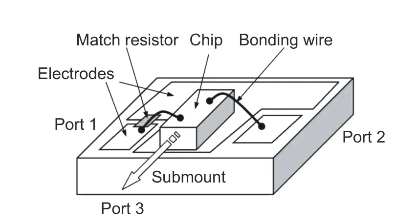
Fig.2.Configuration of integrated EML under test.
As for the scattering parameters,S12andS21,the optical receiver is unnecessary due to the two electrical ports.Instead,a pair of coplanar probes (i.e.,ACP40-GS-200 and ACP40-SG-200) is employed.In this case,the network analyzer can be directly calibrated under the coplanar environment by using the SOLT calibration technique with cascade 103-736 calibration kits.After calibration,S12andS21at the reverse voltages of 0 V and 1 V are obtained when DFB-LD is biased at 70 mA.
4.ModeIing and Discussion
To characterize the microwave interaction between DFB-LD and EAM,an equivalent circuit model of integrated EML was established.For the reason that the submount and the bonding wires will bring parasitics,it is necessary to take the extrinsic parasitic network into account,when modeling the high-frequency behaviors of both DFB-LD and EAM.The parasitic network is usually composed of the package parasitic circuit and the chip parasitic circuit.The package parasitic circuit involves the submount and the bonding wires,which is represented by a pad capacitance,a series inductance,and its resistance.The chip parasitic circuit is associated with the contact capacitance and resistance of the optoelectronic chip[17].Both DFB-LD and EAM can be considered as a cascaded network comprised of the parasitic network and the intrinsic device.Intrinsic DFB-LD is usually modeled by a parallel resistance-inductance-capacitance (RLC)circuit as shown in Fig.3[16],[17].The relaxation oscillation is a resonance between the total capacitanceCtand the inductanceLx,which represents the energy exchange between carriers and photons.Resonance damping is determined by resistancesR1andR2.Meanwhile,intrinsic EAM is a typically parallel resistance-capacitance (RC) circuit as shown in Fig.3,whereRoandCJare the device junction resistance and capacitance,respectively.The resistorRsis the series resistance of the device,including the Ohmic contact resistance at the electrodes and the bulk resistance in the doped semiconductor layers[18].
Intrinsic DFB-LD has a very small input impedance,which can be considered as a short circuit under the above-threshold bias condition[19].Therefore,the parasitic network of DFB-LD can be extracted according to the measured reflection coefficientS22.After the parasitic network is determined,the intrinsic circuit elements of DFB-LD can be easily obtained in sequence by fitting the DFB-LD model to the measuredS32.For EAM,all of the elements values must be extracted simultaneously due to its high impedance characteristics.In this way,the behaviors of DFB-LD and EAM are depicted independently.
Through combining the circuits of DFB-LD and EAM,the fundamental model of integrated EML can be obtained.However,the model is not perfect because the circuits representing the microwave interaction between DFB-LD and EAM have not been considered.Generally,it is necessary to keep proper electrical isolation during fabrication and package of the device.The electrical isolation can be represented by a parallel of the resistance and capacitance.These two elements can be obtained from the measuredS12.After the electrical isolation is determined,the simulatedS21andS12are identical for the reciprocal network.However,this is not the case in the experiment,which indicates that there might be an optical interaction besides the electrical interaction.The optical coupling,from DFB-LD to EAM,absorbs the modulated optical power from the laser and results in additional modulation at the electrical port of the modulator.In the proposed model,the optical coupling is represented by a controlled current source related to the bias current and voltage,and the parameters of the controlled current source are extracted from the measuredS21.
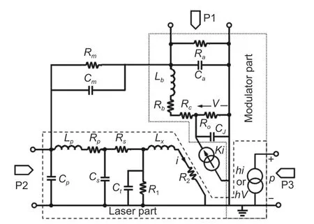
Fig.3.Equivalent circuit model of integrated EML,where the controlled current source and the parallel of Rm and Cm represent the microwave interaction.
All of the measured scattering parameters are shown in Fig.4 to Fig.6,where the corresponding simulation results are shown as the solid lines.For convenience,the values of the circuit elements are listed in Table 1.An advanced design system(Keysight ADS) is used for simulation and the parameter values are gotten through iterating.It is noted that some elements of DFB-LD and EAM,which are determined previously,need to be adjusted and optimized when applying the ultimate simulation to integrated EML with a nonnegligible microwave interaction.
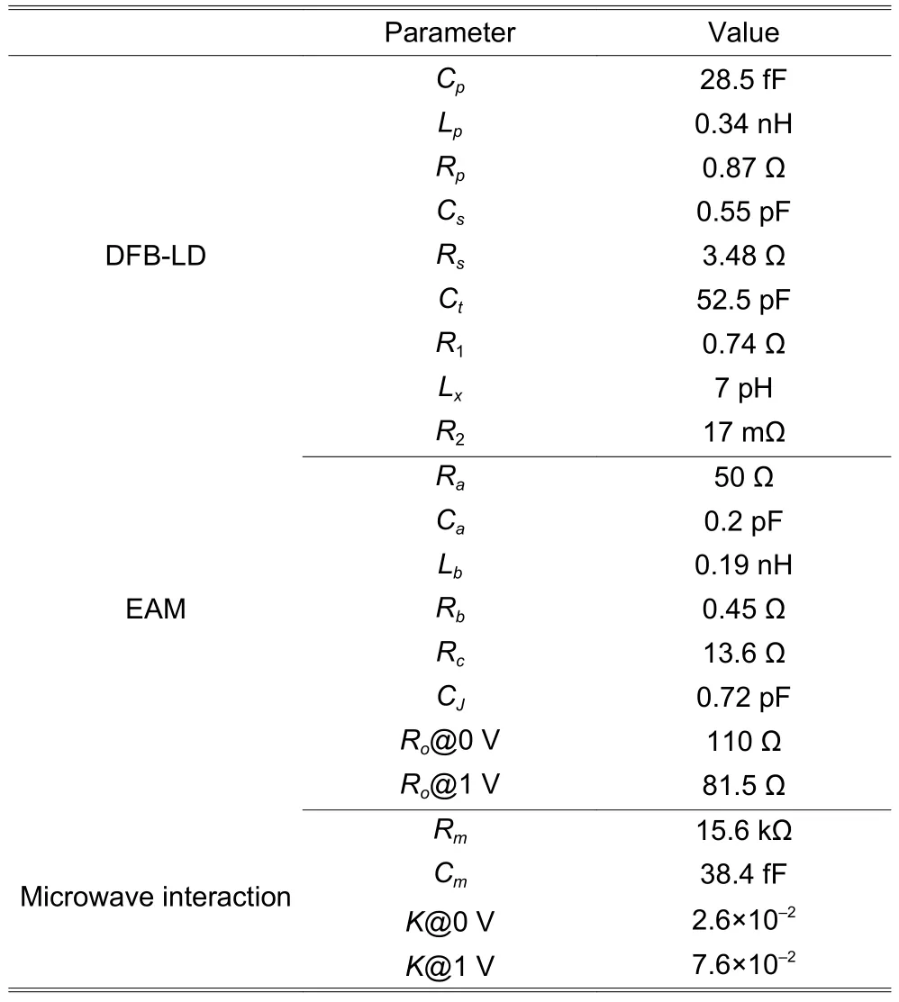
Table 1: Parameter list
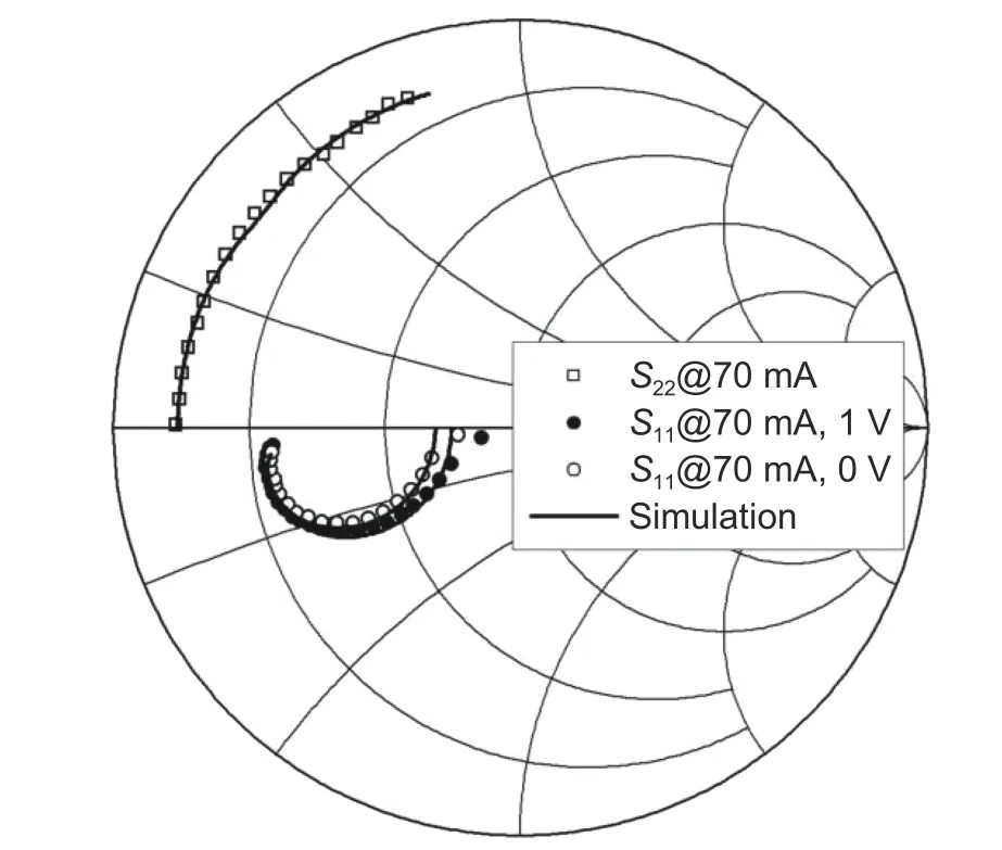
Fig.4.Measured (marks) and simulated (lines) S11 and S22.

Fig.5.Measured (marks) and simulated (lines) S31 and S32.
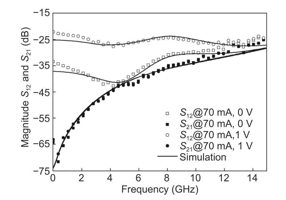
Fig.6.Measured (marks) and simulated (lines) S12 and S21.
As shown in Figs.5 and 6,the reflection and transmission coefficients of EAM vary with the reverse bias voltages due to different electro-absorption efficiency,resulting in differentRoat different bias voltages in the circuit model.From the simulation and measurement results in Fig.6,it can be seen that it is necessary to include the optical coupling in the microwave interaction.Moreover,it can be found that the electrical isolation is bidirectional between DFB-LD and EAM,and the optical coupling is directional from DFB-LD to EAM,which makesS12andS21different.At the low-frequency modulation,the magnitude ofS12is higher than that ofS21because of the high modulation efficiency of DFB-LD.With the increase of the modulation frequency,S12andS21are close to each other gradually.This is because the modulation efficiency of DFB-LD decreases rapidly after the resonance frequency.In this case,the electrical isolation becomes the main contribution to the microwave interaction.
5.ConcIusion
In conclusion,integrated EML was characterized as an electrical-electrical-optical three-port network,from which the scattering matrix was measured to extract the microwave interaction between DFB-LD and EAM.The informative scattering matrix allows us to establish a compact circuit model of integrated EML.Compared with the separate modulator model,the proposed integrated circuit model can be used not only to describe the high-frequency behaviors of EAM,but also to include the effects of DFB-LD.Therefore,the microwave interaction between DFB-LD and EAM can be easily extracted and characterized.Both the simulation and measurement results indicate the microwave interaction includes not only the electrical isolation but also the optical coupling.The electrical isolation is bidirectional,while the optical coupling just works from DFB-LD to EAM.We believe that the characterization on the microwave interaction between integrated DFB-LD and EAM is beneficial for improving the device design and implementing these devices into high-performance inter-and intra-datacenter links.
DiscIosures
The authors declare no conflicts of interest.
杂志排行
Journal of Electronic Science and Technology的其它文章
- PIasma-Enhanced Atomic Layer Deposition of Amorphous Ga2O3 for SoIar-BIind Photodetection
- OrganometaIIic L-AIanine Cadmium Iodide CrystaIs for OpticaI Device Fabrication
- Redox Memristors with VoIatiIe ThreshoId Switching Behavior for Neuromorphic Computing
- ModeIing and SimuIation for Transient ThermaI AnaIyses Using a VoItage-in-Current Latency Insertion Method
- InaudibIe Sound Covert ChanneI with Anti-Jamming CapabiIity: Attacks vs.Countermeasure
- Direction-of-ArrivaI Method Based on Randomize-Then-Optimize Approach
