An FPGA‑based trigger system for CSHINE
2023-01-05DongGuoYuHaoQinShengXiaoZhiQinYiJieWangFenHaiGuanXinYueDiaoBoYuanZhangYaoPengZhangDaWeiSiShiWeiXuXiangLunWeiHeRunYangPengMaTianLiQiuHaiChuanZouLiMinDuanZhiGangXiao
Dong Guo · Yu‑Hao Qin · Sheng Xiao · Zhi Qin · Yi‑Jie Wang · Fen‑Hai Guan · Xin‑Yue Diao ·Bo‑Yuan Zhang · Yao‑Peng Zhang · Da‑Wei Si · Shi‑Wei Xu · Xiang‑Lun Wei · He‑Run Yang · Peng Ma ·Tian‑Li Qiu · Hai‑Chuan Zou,3 · Li‑Min Duan · Zhi‑Gang Xiao
Abstract A trigger system of the general function was designed using the commercial module of CAEN V2495 for heavy-ion nuclear reaction experiments at Fermi energies. The system was applied and verified on the compact spectrometer for heavy IoN experiment (CSHINE). Based on the field-programmable logic gate array technology of the command register access and remote computer control operation, trigger functions can be flexibly configured according to experimental physical goals.Using the trigger system on CSHINE, we conducted a beam experiment at 25 MeV/u 86Kr+124 Sn on the Radioactive Ion Beam Line 1 in Lanzhou, China. The online results demonstrated that the trigger system worked normally and correctly.This system can be extended to other experiments as well.
Keywords CSHINE · Trigger system · FPGA · Heavy ion experiment
1 Introduction
The trigger system is significant for intermediate and highenergy nuclear physics experiments. A well-organized setting of trigger conditions can significantly improve the detection efficiency of physical events of interest and suppress background events. In intermediate-energy heavyion collisions, the final reaction products are abundant and demonstrate 4πemission in the center-of-mass system [1],leading to a significantly rich variety of trigger signals of interest in experiments. Conventionally, the trigger system of an experiment in the Fermi energy domain is composed of independent analog electronic modules, which have the apparent disadvantages of a high power consumption, large space occupancy, inconvenience of remote operation, and lack of scalability. Field-programmable gate arrays (FPGA)are semi-custom circuits in the field of application-specific integrated circuits (ASIC) [2]. This can change the structure of the circuit. Advantageously, it overcomes the nonreconfigurability of application-specific integrated circuits and compensates for the limited number of gate circuits in other programmable logic chips [3]. They have become mainstream programmable logic devices. A trigger system based on FPGA is preferable owing to its advantages of limited space consumption, low power consumption, strong adaptability, and good scalability, and is convenient for remote control operation [4]. Therefore, FPGA-based trigger systems have been gradually adopted in many nuclear physics experiments.
Currently, FPGA have been widely used in experimental signal processing as well as trigger construction, such as the digital signal processing algorithm module [5—8], time-todigital converter (TDC) module [9—11], and trigger modules in experiments [12—15]. For example, FPGA has been successfully used on ATLAS [16, 17], TOTEM [18] and CMS[20] at LHC, real-time track reconstruction at HL-LHC[19], Fermilab SeaQuest experiment [21], MEG experiment[22], LUX dark matter experiment [23], the external target experiment in the HIRFL-CSR [24—28], the CLAS12 experiment [29], and the FTB project [30]. In the aforementioned experiments, the FPGA-based electronic module based on FPGA apparently overcomes the disadvantages of traditional electronics.
This study presents a trigger system based on FPGA technology that adopts the CAEN V2495 VME programmable logic unit [31], which is a general-purpose FPGA and I/O unit housed in a 1-unit wide VME 6U crate. The module performs sequential logic processing on digital signals and digital functions such as coincidence, trigger process, gate and delay generator, and I/O register. Because the electronic module has a flexible function expansion and provides a variety of I/O interfaces compatible with other VME electronic modules, it has been applied to the beam experiment at the compact spectrometer for heavy-ion experiments(CSHINE). Section 2 presents the structure of CSHINE,setup of various types of detectors, and relevant front-end electronics. Section 3 briefly introduces the V2495 module and trigger core logic architecture used in the experiment. In Sect. 4, the performance of the system in the beam experiment is presented, including the timing relationship of the signals involved in trigger construction. Online experimental results are also presented. Section 5 presents a summary of this study.
2 The setup of CSHINE
CSHINE aims to be applied to the experimental studies of heavy-ion reactions and the nuclear equation of state at Fermi energies. It is designed to measure fast fission fragments (FFs) with the coincident emission of charged particles and high-energyγ-rays. In the current configuration,CSHINE consists of the following detectors: (1) four sets of silicon strip detector telescopes (SSDTs) to measure lightcharged particles (LCPs) and intermediate mass fragments(IMFs), (2) three parallel plate avalanche counters (PPACs)to measure the fission fragments, (3) an electromagnetic calorimeter of a CsI crystal (γhodoscope) to record highenergyγrays produced via bremsstrahlung at the early stage of collisions, and (4) a 2 Si(Au) telescope at a small angle to record the elastic scattering of the projectile. The setup of CSHINE for the beam experiment at 25 MeV/u86Kr+124Sn in 2022 is shown in Fig. 1. Each sub-detector is described below.

Fig. 1 (Color online) Schematic diagram of CSHINE setup for beam experiment of 25 MeV/u 86Kr+124Sn
2.1 CSHINE sub‑detectors
The LCPs and IMFs in coincidence with the fission fragments were measured by the SSDTs, each of which was composed of a thin single-sided silicon strip detector(SSSSD) and a thick double-sided silicon strip detector(DSSSD) backed by a 3 × 3 CsI(Tl) crystal array, delivering the energy loss ΔE1, ΔE2, and residual deposited energyECsI, respectively. At the entrance, a 2 μm incident window with an aluminum-coated Mylar film was mounted to stop the delta electrons. The detailed structure of SSDTs can be found in [32]. An adapter made of a PCB plate was mounted at the end of the telescope to connect and transfer the signals of the SSSSD, DSSSD, and CsI array to the front-end electronics. The timing signal (T signal) of the incident particles was extracted from the DSSSD layer. The LCPs and IMFs were identified using the ΔE−Emethod [33].
PPACs were mounted to measure the timing and position information of the FFs emitted in heavy-ion reactions.It is a two-dimensional position-sensitive gas detector composed of a cathode layer in the middle, and mutually perpendicular wire anode layers on both sides. The working gas was C4H10[32]. A negative high voltage was applied to the cathode plane, which delivered a timing signal. The signals induced on the anode planes were transferred to both ends by the delay line, and the time differences were used to deduce the incident position for bothx- andy-dimensions. The first PPAC (PPAC1) is the main fission fragment detector, whereas the second (PPAC2)and third (PPAC3) detectors are installed at the front and middle angles on the other side of the beam as coincident fragment detectors.
Theγhodoscope consisted of 25 CsI(Tl) scintillators in a 5 × 5 configuration. (In the current experiment, only 15 units were installed). The size of each CsI(Tl) scintillator is 70 × 70 × 250 mm3. The optical signal generated in the crystal was collected and amplified by the photomultiplier tubes (PMTs). The high voltage applied to the PMTs ranges from 750 V to 1 kV.
2.2 CSHINE physics goals
The physical goals of CSHINE include but are not limited to the following studies related to the equation of state of asymmetric nuclear matter, that is, the density dependence of the nuclear symmetry energyEsym(ρ) , which is significant in both nuclear physics and astrophysics [34, 35]: (1)The isospin effect of the emission of charged particles in heavy-ion reactions. For instance, the angular distribution of the neutron richness of LCPs reflects the isospin-dependent emission hierarchy and probes the stiffness ofEsym(ρ)[36—40]. Hence, isospin chronology based on the correlation function measurement of particle pairs is required to quantitatively determine the emission sequence of particles with differentN/Zcompositions, from which one can infer the transport of the isospin degree of freedom [41—44] arising from the effect ofEsym(ρ) [45—47]. (2) Studies regarding the dynamic features of the fission process. The properties of the fast fission induced by heavy-ion reactions can be studied by measuring the fission fragments and the coincident LCPs [48, 49], such that the nuclear symmetry energy can be inferred owing to the formation and persistence of the low-density and neutron-rich neck, according to transport model simulations [50, 51]. (3) The high energyγrays emitted in the early stage of heavy-ion collision. As predicted by theoretical simulations, the intensity of high-energyγrays demonstrates a significant dependence onEsym(ρ) [52, 53].Therefore, CSHINE trigger aims to obtain the following types of events: (1) two-body LCPs from the SSDTs for the correlation function measurement, (2) coincidence of two heavy fission fragments in PPACs, defining the fission events, (3) coincidence between fission events and one LCP from SSDTs, (4) coincidence between fission events and oneγ-ray emission, and (5) correlation between onebodyγand one-body LCP. In addition, inclusive events from all the detectors were triggered for detector calibration. The aforementioned requirements define the trigger scheme of CSHINE.
3 System architecture
3.1 Front‑end module
For the SSDTs, the signals from all the channels of the SSSSD, DSSSD, and CsI units were all transferred from the end adapter plate to the Mesytec MPR-16 pre-amplifiers and then successively to the Mesytec MSCF-16 main amplifiers.
At the front panel of each MSCF-16 corresponding to the DSSSDs, one NIM connector delivers a trigger output signal (T-out) if any of the 16 channels is fired. This T-out signal was used as a one-body LCP indicator. In addition,the multiplicity output (M-out) via an NIM connector on the rear panel delivered a linear signal representing the multiplicity of the 16 input channels. The amplitude of M-out wasM×100 mV, whereMis the multiplicity. The M-out signals from all the DSSSD amplifiers are summed further in a linear fan-in and fan-out module to generate anMtotsignal containing the information of the total multiplicity of LCP from all SSDTs. The CF8000 module to receive thisMtotsignal can deliver a trigger for two-body LCP events with a threshold setting above 150 mV [32].
PPAC front-end electronics manage the timing signal T from the cathode and the position signalsX1,X2,Y1, andY2from the anodes of the PPAC detector. The original PPAC signals were first amplified by the ORTEC fasting timing amplifier (FTA 820) and then input to the CF8000 module to generate the NIM logic signals. The timing signal of the CF8000 output corresponding to each PPAC was split into the second path to constitute the trigger signal for fission events. The following two types of coincidences were constructed according to the locations of the three PPACs:PPAC1 and PPAC2 (marked as PPAC1 × 2) and PPAC1 and PPAC3 (marked as PPAC1 × 3) [32, 48]. Because PPAC2 and PPAC3 are located on the same side of the beam, the coincidence between PPAC2 and PPAC3 was not set.
Theγarray is read by photomultiplier tubes (PMTs) with the Hamamatsu R6231. The anode output of each PMT enters the preamplifier CAEN N914, which delivers an energy output and a fast-timing output. While the energy output is fed to the ADC, all the fast time signals of the 15 units are fed into V2495 for two purposes; one is to generate a one-bodyγevent, and the other is to fan-out a signal in the LVDS format, which is converted to ECL and transferred to TDC (V775/N, CAEN) for data acquisition.
3.2 V2495 module
The V2495 module is a CAEN product. It is composed of three FPGA chips, one I/O unit, and a 50 MHz clock crystal oscillator module. It is installed in a one-unit-wide VME 6U standard module [31].
The FPGA architecture of V2495 is shown in Fig. 2. The three FPGA chips are as follows: The main FPGA (MFPGA)is mainly used for the external communication of V2495, for which the VME bus protocol and USB protocol can be used.The user FPGA (UFPGA) chip model is an Altera cyclone V 5CGXC4, which contains 50k logic units, 162 input interfaces, and 130 output interfaces. The Xilinx spartan-6 FPGAchip burns the gate and delay generation (GDG) module.The expansion slot of the I/O module connected to the physical pin of the UFPGA chip in the module enables V2495 to support the input and output of the LVDS, ECL, NIM, and TTL signals by adding three independent sandwich boards[31].

Fig. 2 Architecture of the FPGA connections of V2495
The GDG module is used to control the signal gating,delay, and broadening. The module provides 32 signal interfaces. In the preparation stage of the beam experiment of CSHINE, specific signals generated by the pulser are fed to the front-end electronics of each detector system to simulate the experimental output to conduct timing calibration and test the functions of the trigger module. As an example,Fig. 3 presents the delay of a T signal of PPAC1 in a pulser test. The original signal enters the GDG module and is delayed by 50 ns via remote control.
Because digitization modules are usually located on the experimental site, it is convenient to remotely configure and update the trigger system. Unlike conventional logic electronics, for which users need to pause the beam, access the experimental hall, and locally rebuild the trigger circuit, the V2495-based trigger system advantageously implementsremote operations by adopting the CAEN chain optical network protocol (CONET). The upper computer transmits signals and instructions to V2718 in slot 0 of the VME crate using the PCI/PCIe and CONET protocols. The logic is incorporated into roleplay designer (RPD) files generated by the Quartus II 13.0 compiler. V2718 interacts with V2495 through a VME backplane bus [54].
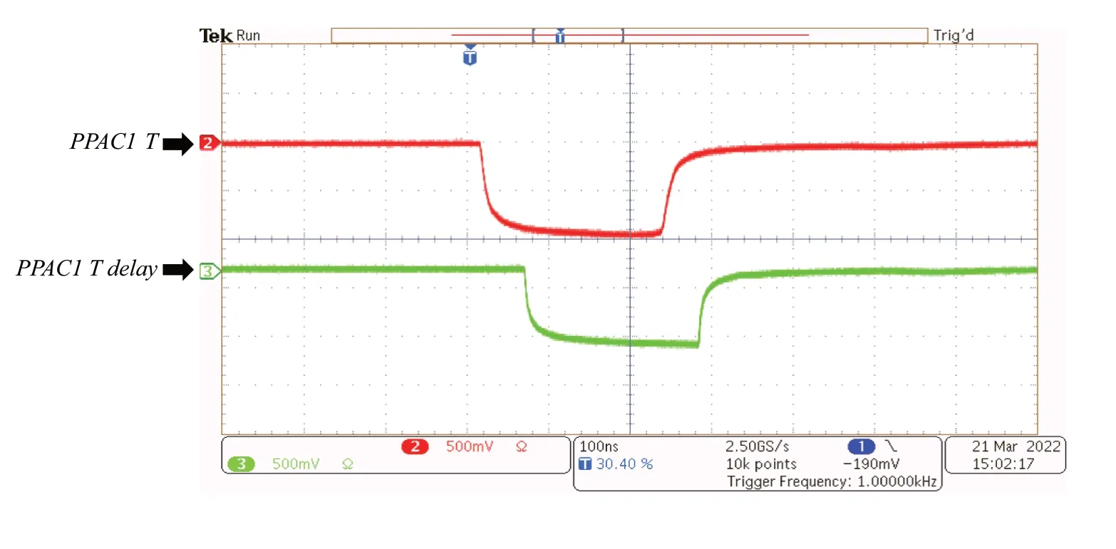
Fig. 3 (Color online) A sample of the oscilloscope view of the timing signal delay of PPAC1.PPAC1 T represents the original signal and PPAC1 T delay represents the output signal after passing through the GDG module
3.3 Trigger signal processing
3.3.1 Trigger logic unit
The logic processing in the trigger system of CSHINE is compiled in Quartus II 13.0 by VHDL, and the remote logic update of the trigger system is achieved in UFPGA by the CAEN electronic firmware upgrade tool CAENUpgrader[31, 55].
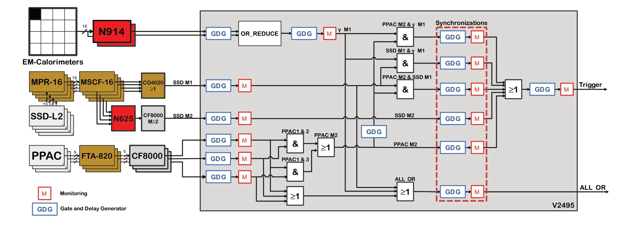
Fig. 4 (Color online) Logic schematic diagram of CSHINE trigger system
Figure 4 presents the logic schematic diagram of the trigger system. The output of the front-end electronics of the subdetectors is used to produce the logic signals before being fed to the trigger module V2495, where the trigger scheme is constructed using the following operations: (1) The fast time signal of the PMTs from N914 is used to generate a one-bodyγsignal (γ M1 ). (2) The fission event signal (PPACM2) is defined by the OR calculation of PPAC1×2 and PPAC1×3 ,corresponding to the coincidence between the main FF detector PPAC1 and the second FF detector, and PPAC2 and PPAC 3, respectively. (3) The two-body LCP signal is provided by the SSDM2 signal. (4) The total one-body trigger signal (ALL OR) for the test and detector calibration is obtained inclusively by the OR operation of the one-bodyγsignal, one-body FF signal from PPAC (PPACM1), and one LCP signal ( SSDTM1). Finally, the global trigger signal of the CSHINE experiment covers the event types listed below, which are enabled by selections or coincidences of the aforementioned signals synchronized by applying a proper delay to each.
• Fission event: PPACM2
• Fission & 1 LCP: PPACM2 AND SSDTM1
• Fission & 1γ: PPACM2 ANDγ M1
• Two-body LCP coincidence: SSDTM2
• LCP &γcoincidence: SSDTM1 ANDγ M1
• Inclusive (All OR): SSDTM1 ORγ M1 OR PPACM1
The advantage of reducing the usage of logical modules in the FPGA-based trigger system is evident. Some NIM logic modules are required to implement the functions shown in Fig. 4 by using traditional electronics. A comparison is shown in Fig. 4 of [42], where the trigger circuit using the NIM modules on CSHINE is shown.
3.3.2 Timing relationship and simulation of signal
To optimize and manage the coincidences in fission events with other types of signals and synchronize various output trigger signals, it is necessary to set an appropriate delay and broadening to all types of triggers via the GDG module, as depicted by the GDG boxes in Fig. 4. Before starting the in-beam experiments, to obtain the correct time sequences of the trigger signal, we conducted simulations for the entire trigger logic scheme within the framework of Quartus II 13.0 and ModelSim 13.0.
In the simulation, the parameters of the delay time and broadening length of the input signals participating in the trigger construction were optimized by considering the response delay of different types of detectors and frontend electronics. For instance, the SSDTM1 signal occurs later than the PPAC timing because the former is extracted from Mesytec MSCF-16. As an example, the parameters of the delay and width for the experiment86Kr+208Pb at 25 MeV/u are listed in Tables 1 and 2. Figure 5 presents the time sequences of the trigger signals with the settings.The PPAC timing signal, SSDTM1 andM2, and theγtiming signal are generated as input signals, where the relative delays to one another are chosen according to the real response of various detectors. With the parameter settings,the trigger signal is shown to be correctly obtained, holding a 300 ns delay to the arrival of the PPAC timing signal.
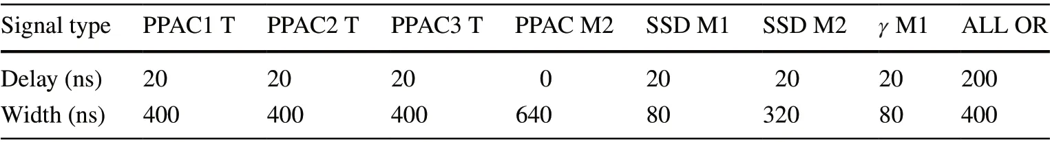
Table 1 Delay and width of each input signal and total onebody trigger signal
3.4 Data acquisition system
A VME standard data acquisition (DAQ) system was used in this experiment. The system was operated based on the following hardware: ADC (V785, CAEN), TDC (V775/N,CAEN), and the CAEN A2818 communication PCI board.The DAQ software was compiled based on C++ on the upper computer, relying on the CAENDigitizer and CAENComm libraries to complete the driver configuration of the DAQ system. An online display of the experimental spectra was achieved by embedding the ROOT library.
The DAQ system responds to the trigger signal in realtime before starting the signal digitization and data transfer.However, if the next trigger signal arrives before the previous signal is completely processed, a data acquisition error occurs. Therefore, it is the responsibility of the user to set up an external interruption circuit for the DAQ system to avoid such conflicts. Figure 6 shows the oscilloscope display of the trigger signal (upper, green) and DAQ busy signal(lower, purple) detected during the beam experiment. Note,the display is in a persistence mode. As shown in the figure,once the first trigger signal arrives, the busy DAQ signal is enabled. During the dead-time period, if the next trigger signal arrives, the system does not respond. As indicated by the arrow in the figure, the second trigger signal is shielded because it arrives during the dead-time. For each triggered event, the total processing time of the DAQ is approximately 200 μ s, depending on the number of firing channels.

Table 2 Delay and broadening of the trigger signals corresponding to different event types

Fig. 5 (Color online) Simulation waveform diagram of trigger signal timing relationship

Fig. 6 (Color online) An oscilloscope view of the trigger signal and DAQ busy signal during the beam experiment.The display is in persistence mode
4 Beam experiment results
During the beam experiment, the timing relationship and time width of the various input and output signals were configured in the trigger system. The trigger condition of the experiment is PPACM2 OR SSDTM2. The fission event is among the trigger conditions because the geometry of the two-body fission events defines the event topology of the physical interest.
Figure 7 presents a typical event with the timing relationship between each detector signal and the total trigger signal obtained during the beam experiment. In this event,PPACM2 corresponding to the fission event (green),γ M1(blue), and SSDTM1 (red) are all presented. As a result, the trigger signal (purple) is correctly generated and delayed by 200 ns from the generation of the PPACM2 signal, which is consistent with the signal simulation results. As expected,the trigger circuit was demonstrated to operate correctly.In this experiment, the total one-body counting rate ranged between 20—40 k (s−1), and the global trigger rate was between 0.5—1 k (s−1) depending on the beam intensity.The DAQ dead time ranged between 80—200 μs.
Online plots were presented to verify the operational status of the trigger system. Figure 8 presents an onlineΔE2−ECsIscattering plot of SSDT4, where ΔE2is from the DSSSD andECsIis from the CsI crystal. The isotopes of theZ≤3 elements can be clearly identified. The forementioned results are consistent with those obtained by the traditional trigger circuit on CSHINE, as shown in Fig 9 of [42]. In addition to the identified isotopic bands,certain heavy backgrounds were visible because the geometric match of DSSSD and CsI was not performed for the online plot. The results demonstrate that the trigger system based on FPGA operates correctly.
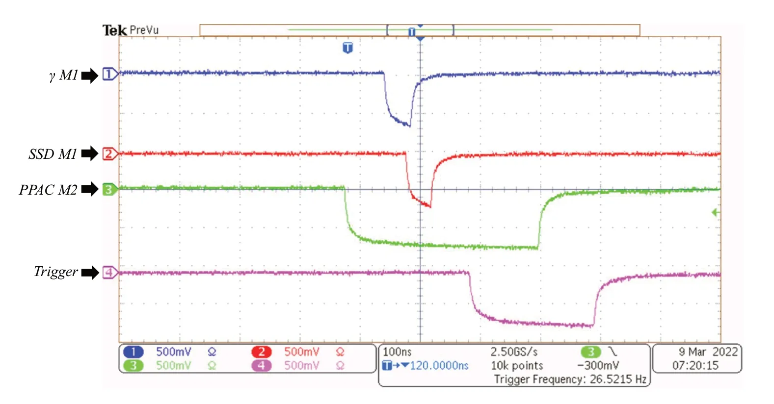
Fig. 7 (Color online) Timing relationship between the input signals and final trigger signal during the beam experiment

Fig. 8 (Color online) Online display of the ΔE2 −ECsI scattering plot of SSDT 4
Figure 9 further demonstrates an onlineγray energy spectrum detected by one unit of theγhodoscope (CsI 5).A peak at 6—8 MeV is presented, of which the origin can be further studied through offiine analyses. In addition,some events were visible in the high-energy region beyond the beam energy (25 MeV/u). If these high-energyγ-rays are verified by a careful offiine analysis, it may provide insight into the production mechanism of the bremsstrahlungγrays in heavy-ion reactions.

Fig. 9 (Color online) Online display of the γ ray energy spectrum of CsI 5 in the beam experiment
5 Conclusion
An expandable trigger system that meets the physical requirements was designed for CSHINE. The system adopts a V2495 logic unit and achieves trigger functions in the FPGA equipment. By designing and modifying trigger functions according to user commands or the online reconfiguration of the FPGA, the signal timing sequences meet the experimental requirements and a good flexibility of the system can be guaranteed. The functionality of the system was demonstrated in a beam experiment using CSHINE on RIBLL1 in 2022. This study provides a practical trigger solution for CSHINE and other nuclear physics experiments on a similar scale.
Author ContributionsAll authors contributed to the study conception and design. Material preparation, data collection and analysis were performed by Dong Guo and Yu-Hao Qin. The first draft of the manuscript was written by Dong Guo, and all authors commented on previous versions of the manuscript. All authors read and approved the final manuscript.
杂志排行

Nuclear Science and Techniques的其它文章
- Analysis on the influencing factors of radioactive tritium leakage and diffusion from an indoor high‑pressure storage vessel
- Structural integrity evaluation of irradiated LEU targets for the production of molybdenum‑99 using thermo‑mechanical behavior simulation coupled with pressure of fission gas release calculation
- A method for neutron-induced gamma spectra decomposition analysis based on Geant4 simulation
- Prediction of nuclear charge density distribution with feedback neural network
- Two‑parameter dynamical scaling analysis of single‑phase natural circulation in a simple rectangular loop based on dilation transformation
- Multiple-models predictions for drip line nuclides in projectile fragmentation of 40,48Ca, 58,64Ni, and 78,86Kr at 140 MeV/u