Nano Ag-enhanced photoelectric conversion efficiency in all-inorganic,hole-transporting-layer-free CsPbIBr2 perovskite solar cells
2022-12-28YoumingHuang黄友铭YizhiWu吴以治XiaoliangXu许小亮FeifeiQin秦飞飞ShihanZhang张诗涵JiakaiAn安嘉凯HuijieWang王会杰andLingLiu刘玲
Youming Huang(黄友铭) Yizhi Wu(吴以治) Xiaoliang Xu(许小亮) Feifei Qin(秦飞飞) Shihan Zhang(张诗涵)Jiakai An(安嘉凯) Huijie Wang(王会杰) and Ling Liu(刘玲)
1Tiangong University,Tianjin 300387,China
2University of Science and Technology of China,Hefei 230026,China
3Nanjing University of Posts and Telecommunications,Nanjing 210003,China
4Shanxi Normal University,Shanxi 041004,China
Keywords: Ag nanoparticles,local surface plasmons,perovskite solar cells based on CsPbIBr2
1. Introduction
With a decline in fossil energy resources (i.e., oil and coal) leading to a global energy crisis and the environmental pollution associated with these fossil fuels, the demand for clean and sustainable energy sources has become an important topic of growing concern for all. Solar cells convert the inexhaustible energy of the sun into electricity,representing one of the most promising solutions for harnessing solar energy.[1,2]Perovskite solar cells(PSCs)have attracted much attention due to their advantages of low production cost and simple fabrication. The power conversion efficiency (PCE)of PSCs has improved from 3.81% in 2009 to 25.7%[3–8]in 2022. The light absorption layer of highly efficient PSCs mostly contains organic groups. These organic groups are easily degraded in high-temperature, high-humidity environments,which restricts the development of organic PSCs.[9,10]Researchers have therefore turned their attention to the field of all-inorganic PSCs which have much better stability. Allinorganic PSCs based on CsPbIBr2material have excellent stability and stand out among the various types of all-inorganic PSCs. Maet al.[11]first reported CsPbIBr2-based PSCs, and achieved a PCE of 4.7%. Yanget al.[12]modified the surface of CsPbIBr2film with bifunctional dye molecules,and the optimized perovskite solar cells achieved an open circuit voltage(VOC)of 1.37 V and a PCE of 10.13%.
In 2021, Duet al.[13]used (NiCo)1−yFeyOx-decorated graphene oxide (GO) as a hole booster in an all-inorganic CsPbIBr2PSC. A best efficiency of 10.95% was achieved,arising from the charge transfer doping effect between(NiCo)1−yFeyOxand GO. According to the latest report, the PCE of hole transport layer (HTL)-free carbon electrode CsPbIBr2perovskite solar cells has reached 11.04%,[14]but this is still far from the current maximum efficiency of PSCs.It can be seen that CsPbIBr2-based PSCs have good stability, but their PCE is low. The absorption of incident light by PSCs has an important influence on device performance.Therefore, the performance of CsPbIBr2-based PSCs can be improved by improving the absorption of incident light by these devices. Many attempts have been made to improve the performance of the PSCs,including modification of the lightabsorbing layer or doping of photoactive nanostructures.[15–17]Atwater and Polman[18]described the physical mechanism by which surface plasmon resonance (SPR) of metal nanostructures enhances the light absorption of solar cells, mainly including light scattering by metal nanoparticles (NPs) and near-field enhancement of the localized surface plasmon resonance (LSPR), which can be applied to solar cells. In recent years, SPR has been used in many fields.[19]Although LSPR of metal NPs is used to enhance the absorption of incident light by PSCs,there has been relatively little research work on this.[20–22]
Wanget al.[23]and Leeet al.[24]have demonstrated the incorporation of Au NPs into the HTL of photovoltaic (PV)devices. Their results show that the SPR characteristics of Au NPs can greatly improve the light absorption capacity and photocurrent density of cell devices, accompanied by a small reduction in photovoltage. Cuiet al.[25]and Zhanget al.[26]incorporated Au NPs into the electron transport layer (ETL)of PSCs. The metal nanostructures in solar cells not only increase the optical path of light scattering[27,28]but can also could produce dipole–dipole interaction and resonance energy transfer,[29]which is expected to improve the PCE of PV devices. There have been no reports about metal NPs enhancing CsPbIBr2-based PSCs.
In this work, Ag NP enhancement of CsPbIBr2-based PSCs with the structure FTO/(Ag)ZnO/CsPbIBr2/carbon(FTO is fluorine-doped tin oxide) is investigated. Different devices are obtained by controlling the surface coverage ratio (SC) of Ag NPs on the FTO surface. In this paper SC is defined as the proportion of the solar cell area with Ag NPs compared with the total solar cell area. When SC=10%the CsPbIBr2-based PSC achieves its best PCE of 2.7%,which is 9.76%higher than that of the control cells. Moreover,we use the finite difference time domain(FDTD)method to simulate the structure of our designed solar cell devices. The model devices with different Ag NP SCs are obtained by controlling the interval size of Ag NPs on the FTO substrate surface. The simulated transmittance, reflectance and absorptivity and also the simulated electric field distribution of each cross section are obtained using FDTD. We further analyze the Ag NP-enhanced CsPbIBr2PSCs. It is demonstrated that the near field enhancement and forward scattering of Ag NPs can enhance the performance of CsPbIBr2-based PSCs.To the best of our knowledge, there have been no reports using this method to improve the device performance of such CsPbIBr2PSCs. Ag NPs were chosen from among various metal NPs(Au, Ag, Al, etc.) due to their low price and relatively good controllability in the synthesis process.[30,31]
2. Experimental methods
2.1. Materials
AgNO3(99.8%) was purchased from Tianjin Yingda Sparseness & Nobel Reagent Chemical Factory. Acetone(99.5%), ethyl alcohol (EtOH; 99.7%) and sodium citrate trihydrate (99%) were purchased from Tianjin Fengchuan Chemical Reagent Technology Co., Ltd. ZnO ceramic target (99.99%) was purchased from Zhongnuo New Material(Beijing) Technology Co., Ltd. Lead (II) bromide (PbBr2;99. 99%) and cesium iodide (CsI; 99.99%) were purchased from Xi’an Polymer Light Technology. Dimethylsulfoxide(DMSO;99.8%)was purchased from Aladdin.FTO glass substrates (7 Ω) were received from Luoyang Guluo Glass Co.,Ltd.Commercial conductive carbon paste was purchased from Shanghai MaterWin New Materials Co.,Ltd. All these chemicals and reagents were used directly without any further purification.
2.2. Device fabrication
Figure 1 shows a flow chart of the laboratory preparation of enhanced CsPbIBr2-based PSCs. After boiling 150 mL of AgNO3solution (mass fraction 0.018%), 2 mL of sodium citrate trihydrate solution(mass fraction 2%)was added. This was stirred evenly and boiled then washed with EtOH several times, followed by dispersion in EtOH for 3 min to obtain Ag NPs with a diameter for about 150 nm. FTO glass was cleaned ultrasonically for 15 min in deionized water, acetone and EtOH, then dried with nitrogen. The FTO glass was put into a plasma cleaning machine for 10 min and the Ag NP solution was directly dripped onto the cleaned FTO surface.Three different Ag NP SC surfaces were obtained by controlling the amount of solution. ZnO films were deposited onto the FTO by radio-frequency sputtering. The sputtering time was 60 min, the sputtering power was 50 W, the flow rate of argon (purity 99.99%) was 14 sccm and the working pressure was 3 Pa. After plasma cleaning of FTO with ZnO films,CsPbIBr2films were deposited on the ZnO films in a glove box using one-step spin coating. Then 50µL of CsPbIBr2precursor solution was dropped on the ZnO film and the substrate rotated. For the spin coating, the rotation speed of the stage was 3000 rpm for 40 s. The above samples were annealed at 160◦C for 20 min. The CsPbIBr2precursor solution was prepared according to the literature: 370 mg PbBr2and 259 mg CsI were dissolved in 1 mL of DMSO at room temperature.Finally,carbon electrodes were deposited on the CsPbIBr2layer as the HTL and back electrodes and annealed at 100◦C for 20 min. The active area of each device was 0.20 cm2.
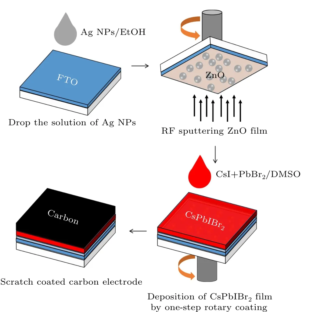
Fig. 1. Flowchart for preparing enhanced CsPbIBr2-based PSCs in the laboratory.
2.3. Characterization
Surface morphologies of the films were analyzed using a field emission scanning electron microscope(SEM;Gemini 300). Photoluminescence spectra (PL) were recorded using a fluorescence spectrometer (Hitachi, F7000). Ultraviolet–visible (UV–vis) absorption spectra were recorded using a UV–vis near-infrared spectrophotometer (PerkinElmer,Lambda 35). TheJ–Vcurves of the CsPbIBr2-based PSCs were obtained using a Keithley 2400 source meter under AM 1.5 G illumination at 100 mW·cm−2(Newport Oriel Sol3A),which was calibrated using a standard silicon solar cell. Measurements of external quantum efficiency (EQE) were performed using a quantum efficiency measurement system(QER,EnliTech)in the 300 nm–700 nm wavelength range.
3. Results and discussion
The SEM image of Ag NPs prepared on the surface of the FTO substrate is shown in Fig. 2(a). Spherical Ag NPs with a diameter of about 150 nm can be seen. The UV–vis absorption spectrum of Ag NPs in EtOH is shown in Fig. 2(b). It can be seen that the Ag NP structure has a specific SPR absorption peak at about 475 nm. A SEM image of Ag NPs agglomerated and stacked on the FTO substrate is shown in Fig.2(c). As shown in Fig.3(a),when SC=5%,Ag NPs on the surface of the FTO substrate are sparsely distributed and relatively uniform.As the SC of the Ag NPs increases to 10%,the Ag NPs on the surface of the FTO substrate show local aggregation(see Fig.3(b)),but are still monolayer structures.When SC further increases to 15% (Fig. 3(c)), a large number of Ag NPs on the surface of the FTO substrate become aggregated into clusters. It can be seen that Ag NPs accumulate with increasing SC; we believe that the reasons for this phenomenon are the uneven distribution of NPs accompanied by solvent volatilization and the increase in the number of Ag NPs,which may be caused by anisotropy of the FTO substrate.
The UV–vis absorption spectra of the ZnO/CsPbIBr2film when SC=10% and SC=0% are shown in Fig. 4(a). Both show similar absorption characteristics within the visible spectrum (400 nm–700 nm), and their absorption edges are in the same position. In the visible light range of 400 nm–700 nm,the ZnO/CsPbIBr2film(SC=10%)has a stronger absorption intensity, which could be attributed to spectral overlap between CsPbIBr2films and plasmon resonance of Ag NPs.[32,33]Correspondingly,more photocarriers are generated,which is conducive to an increase in the short circuit current densityJsc. The PL spectra of the ZnO/CsPbIBr2film at SC=10% and SC=0% are shown in Fig. 4(b). It can be seen that the emission peaks of both samples are at 605 nm.The emission peak intensity of the SC=10%sample is higher than that of the SC=0%one.The SC=10%sample achieved an integrated PL intensity of 9.40 arb. units compared with 8.14 arb. units for the sample without Ag NP doping, an increase of 15.48% in integrated PL intensity. The surface of Ag NPs has a strong local field which increases the photon density and the excited state density in the device. As a result, the number of electron–hole pairs increases, radiation recombination is enhanced and fluorescence intensity is improved. The increase in the PL intensity of perovskite films on the ZnO with SC=10% is due to the above reasons. It has been proved that SPR can improve PL intensity.[33]It is useful to boost theVOCof PSCs because theVOCof solar cells is positively correlated with the emission peak intensity of the light absorption layer.[34,35]In Fig. 4(b), there are many peaks besides the main peak in the PL spectrum; we believe that this phenomenon is caused by defect luminescence of ZnO materials and perovskite materials. The cross-sectional SEM image of the carbon-based CsPbIBr2PSC device is presented in Fig. S1 and a layered structure can be clearly identified. We show the energy level schematic diagram of the FTO/(Ag)ZnO/CsPbIBr2/carbon solar cell in Fig.5.

Fig.2. (a)SEM image of Ag NPs on the FTO substrate. (b)Uv–vis absorption spectra of Ag NPs. (c)SEM image of Ag NPs agglomerated and stacked on the FTO substrate.

Fig.3. SEM images of a FTO substrate with different Ag SCs: (a)SC=5%,(b)SC=10%,(c)SC=15%.
We changed the particle SC of Ag NPs on the FTO surface and then prepared the devices. Table S1 shows the parameters of each device. As the Ag NP SC increased from 0 to 10%,the PCE of PSCs increased from 2.46%to 2.70%. When the SC is 10%, the solar cell achieves its best performance.ItsVOCis 0.8 V,Jscis 8.02 mA·cm−2and FF is 0.42. These enhancements are mainly due to the introduction of Ag NPs,which improve the light absorption of the CsPbIBr2PSC and finally turn into excess photogenerated carriers. In addition,perovskite is a direct band gap material; it is easy to recombine radiation and re-emit usable photons to realize the photon cycle effect.[36,37]As the addition of Ag NPs gives the film a higher fluorescence intensity, the generation and separation ability of photogenerated carriers can be improved through the photon cycle effect. The improvement of the sample with SC=5% is not so obvious because there are insufficient Ag NPs to excite the surface plasmons. However, as the Ag NP SC further increases to 15%,the PCE of the PSC decreases to 1.27%. In this condition, too many Ag NPs on the surfaces(Fig. 3(c)) hinder light from entering into the CsPbIBr2and decrease the absorption of incident light.
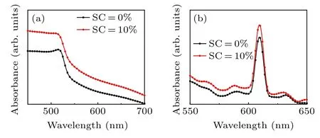
Fig.4. UV–vis absorption spectra of ZnO/CsPbIBr2 thin films with different Ag SCs. (b)PL spectra of ZnO/CsPbIBr2 thin films with different Ag SCs.
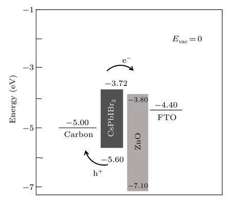
Fig.5. Corresponding energy band diagrams of CsPbIBr2 PSCs.
Figure 6(a) shows theJ–Vcurve of the device when the Ag NP SC is 10%and 0%.When the AgNP SC is 0%,theVOCof the device is 0.72 V and theJscis 7.46 mA·cm−2. TheVOCandJscof the device with SC=10% increased to 0.8 V and 8.02 mA·cm−2, respectively. This indicates that the addition of Ag NPs improves the performance of the device.
The EQE curves of the corresponding solar cells are illustrated in Fig.6(b). It can be seen that the spectral response range of both devices is roughly in the 300 nm–600 nm wavelength range. The EQE value of the device with SC=10%is higher than the device without Ag NPs. Furthermore, across the optical response range, the maximum EQE of the device with SC=10%is 66.57%,which is significantly higher than that of the device (63.20%) without Ag NPs. The improved EQE value facilitates the enhancement of the photoelectric conversion properties.
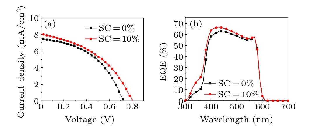
Fig.6. (a)Current density–voltage(J–V)characterization of PSCs with different Ag SCs. (b) External quantum efficiency (EQE) characterization of PSCs with different Ag SCs.
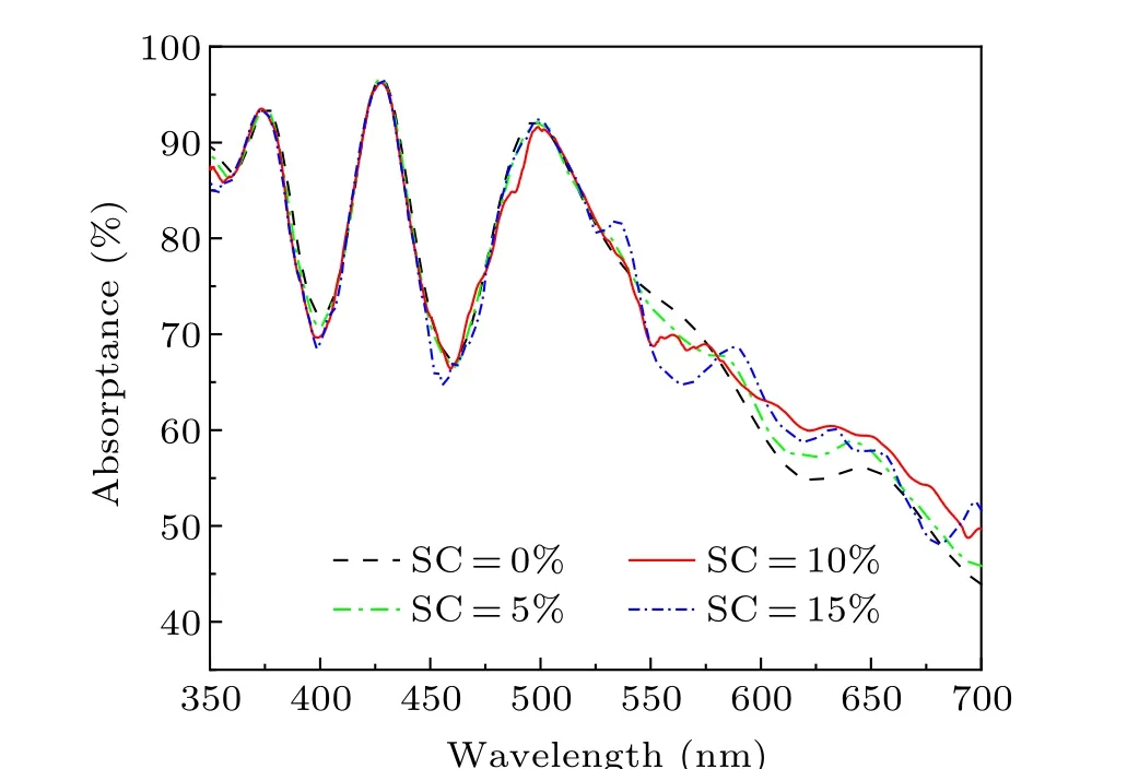
Fig.7. Simulated absorptance of the samples with different Ag SCs.
To further investigate the influence of the near-field enhancement of the LSPR by Ag NPs on the performance of PSCs, a 3D model was established using the FDTD method. The ‘Johnson and Christy’ model was adopted for the Ag NPs. The numerically simulated device structure(see Fig. S2(a)) is glass/FTO (350 nm)/ZnO (200 nm)/CsPbIBr2(250 nm)/carbon and the spherical Ag NPs are embedded at the FTO/ZnO interface. The numbers in brackets represent the actual thickness of the corresponding layer.
As shown in Fig.S2(a),perfectly matched layer boundary conditions were used in thez-direction and periodic boundary conditions were used in thex/y-direction. The diameter of Ag NPs was set to 150 nm and different SCs were used. The SC can be obtained by changing the intervals between two particles.Figure S2(b)shows thex–zplane(y=0)and the monitoring positions of eachx–yplane. The simulated transmittance of the samples with different Ag SCs is shown in Fig. S3(a).When Ag NPs are put on the FTO surface the transmittance decreases with increasing the Ag NP SC,which may increase the blocking of incident light. Figure S3(b) shows the simulated reflectance of the samples with different Ag SCs. The sample without the addition of Ag NPs has the lowest reflectance.According to the simulated reflectivity and transmittance, it can be inferred that the absorption rate of the device increases with increase of in SC.The monitoring positions of reflectivity and transmittance refer to Fig.S2(a).
The absorptance of different samples was plotted according to Fig. S3, as shown in Fig. 7. It can be seen that the position of the absorption peak is about 425 nm. As can be seen in the figure, the absorbance of the sample without the addition of Ag NPs is lower. In addition,the absorptance with SC=15% is lower than that with SC=10%, indicating that excessive Ag NPs will reduce the absorption of incident light.
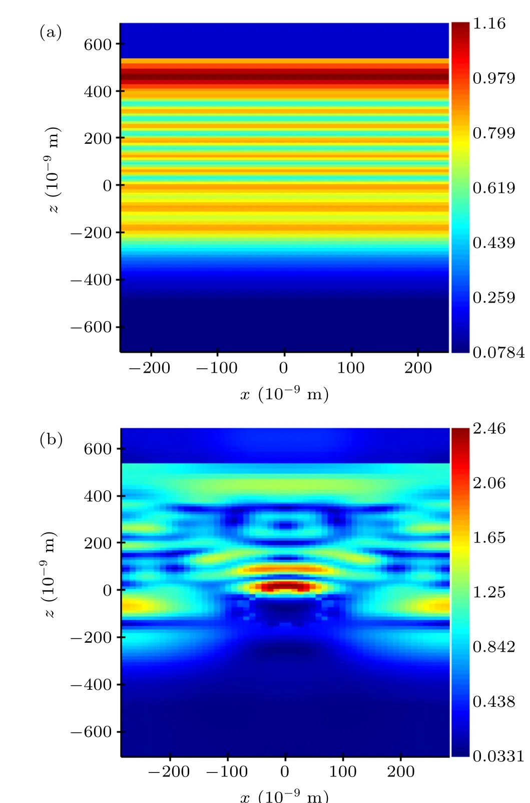
Fig. 8. Simulated electric field distribution (λ =425 nm) in the x–z plane(y=0): (a)SC=0%,(b)SC=10%.
The simulated electric field distribution with an excitation wavelength of 425 nm is shown in Figs. 8 and 9. Hereλ=425 nm due to its position close to the resonance absorption peak of Ag NPs,and it has higher absorptance than with other wavelengths. Figures 8(a) and 8(b) are the simulated electric field distributions of the devices with SC=0% and SC=10% atλ=425 nm, where all figures are in thex–zplane (y=0). As shown in Fig. 8(b), the electric field intensity of the CsPbIBr2layer of the device with SC=10% is greater than that of the SC=0%device. More incident light would be absorbed because the rate of absorption of light is proportional to the intensity for a given wavelength. Figure 8 is divided into three areas: (i) 0 nm Figure 9 shows the simulated electric field distribution on thex–yplane for different values ofz. The monitoring positions on eachx–yplane correspond to (i), (ii), and (iii), respectively, in Fig. S2(b). Figures 9(a) and 9(b) show that the electric field intensity of the device (forz=−205 nm) with SC=10%is significantly higher than that of the device with SC=0%; this indicates that the absorption of incident light is improved. As shown in Figs. 9(c) and 9(d), the electric field intensity of the device(forz=−350 nm)with SC=10%is significantly higher than that of the device with SC=0%.Compared with Fig. 9(b), the areas in Fig. 9(d) where electric field intensity significantly increased were at the edge of the plane. Figures 9(e) and 9(f) show that the electric field intensity of the device (forz=−450 nm) with SC=10% is significantly higher than that of the device with SC=0%. The form of electric field enhancement shown in Fig.9(f)is similar to Figs.9(b)and 9(d), but the blue region in the center of the plane is larger. The blue areas in the center of the plane in Figs.9(b),9(d),and 9(f)are the area below the Ag NPs in the model. As this area is shielded by Ag NPs it cannot be irradiated by incident light. Compared with other areas, the blue area absorbs less incident light,resulting in a low electric field intensity. However, the electric field intensity around the blue region is significantly enhanced compared with that in other areas,due to the forward scattering of the incident light by the Ag NPs. The reason for this phenomenon is that after incident light is scattered forward by Ag NPs, the scattered light path intersects with other incident light paths on the plane. The light-absorbing layer therefore absorbs more incident light energy and hence could stimulate more photocarriers in the CsPbIBr2layer. It can be seen from Figs. 9(b), 9(d) and 9(f)that the blue area in the samex–yplane increases with the location of the monitoring plane away from the ZnO/CsPbIBr2plane. The above phenomenon shows a distinct angular distribution,which is consistent with the forward-scattering feature in Fig. 8(b). As is generally known, the forward-scattering effect of Ag NPs is an important factor that improves the performance of devices. Moreover,it can be seen from Figs.9(b),9(d)and 9(f)that the electric field around the blue area of the plane is not uniform, and the electric field in the region not affected by the forward-scattering effect is also increased,indicating that enhancement of the electric field cannot simply be attributed to the forward-scattering effect of Ag NPs but is also related to the near-field enhancement of the LSPR.Therefore,it is reasonable to believe that the enhancement of device performance is caused by the near-field enhancement of the LSPR and forward scattering of Ag NPs. Fig.9. Simulated electric field distribution(λ =425 nm)in x–y plane below the CsPbIBr2 layer: (a),(b)z=−205 nm;(c),(d)z=−350 nm;(e),(f)z=−450 nm. (a),(c),(e),(g)SC=0%;(b),(d),(f),(h)SC=10%. In summary, we conducted experimental and numerical simulation studies on Ag NP-enhanced all-inorganic hole-free PSCs based on CsPbIBr2materials. The near-field enhancement and forward scattering of Ag NPs are utilized to improve the absorption of incident light and enhance the performance of the device. When a Ag NP solution was dropped on the surface of FTO, the PCE of the PSCs reached 2.70%when SC=10%,which was 9.76%higher than that of devices with SC=0%. We can understand the experimental results through numerical simulation using the FDTD method. Considering the feasibility of this technology,our experiment provides a method for improving the efficiency of all-inorganic PSCs based on CsPbIBr2materials. Acknowledgments Project supported by the National Natural Science Foundation of China(Grant Nos.11504264,21802092,51501128,52072005, and 51872279) and the Scientific Research Plan Project of Tianjin Municipal Education Commission (Grant No.2017KJ097).
4. Conclusion
猜你喜欢
杂志排行
Chinese Physics B的其它文章
- Fault-tolerant finite-time dynamical consensus of double-integrator multi-agent systems with partial agents subject to synchronous self-sensing function failure
- Low-voltage soft robots based on carbon nanotube/polymer electrothermal composites
- Parkinsonian oscillations and their suppression by closed-loop deep brain stimulation based on fuzzy concept
- Temperature dependence of spin pumping in YIG/NiO(x)/W multilayer
- Interface effect on superlattice quality and optical properties of InAs/GaSb type-II superlattices grown by molecular beam epitaxy
- High-sensitive phototransistor based on vertical HfSe2/MoS2 heterostructure with broad-spectral response
