不同Ge 组分a-Si1-xGex键合层对InGaAs/Si 雪崩光电二极管性能的影响
2022-10-25周锦荣鲍诗仪佘实现黄志伟柯少颖
周锦荣,鲍诗仪,佘实现,黄志伟,柯少颖
(闽南师范大学物理与信息工程学院,福建漳州 363000)
0 Introduction
APD is a semiconductor optoelectronic device with internal photocurrent gain[1].It has been widely employed in various application fields,i.e.,fiber-optic transmission systems[2],laser ranging,infrared imaging[3],single-photon detection[4],and quantum communication[5].Nowadays,APD is an attractive device attributed to its advantages of high responsivity,high sensitivity,and low noise[6].The current mainstream APD is based on InGaAs/InP material[7].High-quality InGaAs film can be directly grown on InP material by epitaxial recipe[8]attributed to the matched lattices between InGaAs and InP[9].However,It is difficult to reduce noise(dark current)significantly ascribed to the fact that InP material suffers from a highkvalue(0.4~0.5)[10].
To improve the performance of APD,researchers proposed to replace InP material with Si material.Si material is widely selected for APD applications due to its lowkvalue(0.02)[11].On the other hand,due to the high crystal quality of Si material[12],the dark current of InGaAs/Si APD theoretically should be much lower than that of InGaAs/InP APD.Nevertheless,ascribed to the significant lattice mismatch between InGaAs and Si[13],it is not easy to directly grow high-quality InGaAs film on Si material using an epitaxial technique[14].Although it was reported that applying the direct fusion wafer bonding technique to achieve bonding of InGaAs and Si,this technique cannot completely isolate the lattices.To significantly eliminate the effect of lattice mismatch,an amorphous semiconductor material layer,such as a-Si1-xGex(a-SiGe)material with different Ge content(different bandgap),is inserted at InGaAs/Si interface(SIB method).The a-SiGe[15]without crystal orientation can significantly reduce the valence band offset due to its adjustable bandgap with different Gecomponent.The dislocation nucleation is eliminated by the amorphous bonding layer,thereby alleviating the effect of lattice mismatch between InGaAs and Si.However,the effect of the a-SiGe bonding layer on the performance of the wafer-bonded InGaAs/Si APD,especially on the feature of carrier transport at the bonded interface,is still unclear.
In this paper,we theoretically insert an a-SiGe layer at the InGaAs/Si bonded interface to simulate the effect of the bandgap of a-SiGe with different Ge content on the performance of the APD.The recombination rate,electric field,tunneling rate,carrier concentration,energy band,and carrier velocity as a function of the Ge content are extracted for comparison.The 3 dB bandwidth of the device decreases as the bandgap increases due to the blocking effect at the bonded interface.The gain of as high as 30 is obtained,and the Gain-Bandwidth Product(GBP)of 60 GHz is achieved,which is close to that of InGaAs/InP APD.The dark current(~10-10A@95%breakdown voltage)exhibits a meager value at room temperature,much lower than the InGaAs/InP APD.
1 Parameter setting
The theoretical simulation of InGaAs/Si APD is based on the three basic equations of carrier migration in semiconductors:Poisson's Eq.(1)[16],current continuity Eq.(2)and Eq.(3),and carrier transport Eq.(4)and(5).Besides,the bandgap narrowing[17],optical composite[18],defect-assisted tunneling[19],concentrationdependent Shockley-Read-Hall Eq.(6)[20],Auger recombination Eq.(7),Non-local Quantum Barrier Tunneling Eqs.(8)~(10),and Selberherr’s Impact ionization Models Eq.(9)[21]are conducted to explore the factors that affect the performance of the InGaAs/Si APD.
Whereεrepresents the electrostatic constant,ψrepresents the electrostatic potential energy,andρrepresents the volume density of the charge.
whereGpandGnboth represent the generation rate of carrie and electron.RnandRprepresents the recombination rate of hole and electron.
whereJnandJprepresent transport current of densitie hole and electron,qrepresents unit charge,μnandμprepresent carrier mobility of an electron,prepresents carrier concentration,φnandφprepresent the quasi-Fermi level of N-type and P-type semiconductors,respectively.
whereAandCrepresent the recombination coefficients of SRH generation recombination and Auger recombination,respectively.niis the intrinsic carrier concentration.
Due to the barrier at InGaAs/Si bonded interface when a-SiGe bonding layer is inserted,a non-local quantum barrier tunneling model which can calculate the tunneling current through the quantum barrier between InGaAs and Si is used.For direct bandgap material,the tunneling current is given by
wheremyandmzare the density of states effective mass,EFrandEFlare the quasi-Fermi levels on either side of the barrier,T(E)is the tunneling probability.For indirect bandgap material,the tunneling current is given by
wheremtis the transverse effective mass,mlis the longitudinal effective mass,mlhandmhhare the light hole and heavy hole effective mass,respectively.The Selberherr's impact ionization model was introduced in the program.The electron and hole ionization rates are expressed as
whereEis the electric field in the direction of current flow at a particular position in the structure.The userdefinable parameters AN,AP,BN,and BP of InGaAs and a-SiGe are listed in Table 1.Egran is the electric field value,when the electric field is higher than Egran,the parameters of AN1,AP1,BN1,and BP1 are used.Otherwise,the parameters of AN2,AP2,BN2,and BP2 are used.
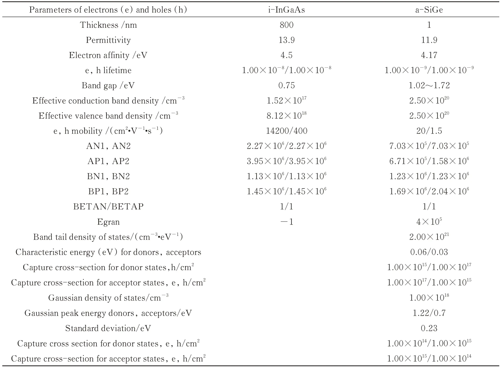
Table 1 Parameter set for the simulation of InGaAs/Si APD with Atlas
2 Simulation results
The schematic diagram of the wafer-bonded InGaAs/Si APD is shown in Fig.1.One can see that the InGaAs layer includes a heavily-doped p-type InGaAs contact layer(0.1 μm),i-InGaAs absorption layer(0.8 μm),and i-InGaAs grading layer(0.08 μm).The InGaAs contact layer is connected to the electrode.The InGaAs absorption layer absorbs the near-infrared light(1 550 nm).The role of the InGaAs grading layer is to reduce the band offset between InGaAs and Si.Due to the lattice mismatch,the a-SiGe bonding layer acts as a lattice blocking layer to eliminate the nucleation of threading dislocations between InGaAs and Si.Because the a-SiGe layer is an amorphous material,thick a-SiGe layer may lead to serious recombination at the bonded interface,leading to the deterioration of the performance of the device.Thus,the thickness of the a-SiGe layer is set to be 1 nm,which is suitable for the interlayer wafer bonding.The Si layer includes a lightly-doped ptype Si charge layer(0.1 μm),i-Si multiplication layer(0.5 μm),and heavily-doped n-type Si contact layer(1 μm).The charge layer plays a role in modulating the electric field of the absorption layer and avalanche layer to form a high electric field in the Si multiplication layer to trigger drastic impact ionization and a low electric field in the InGaAs layer to restrain the impact ionization.Thus,the noise of the APD derived from the impact of holes can be restrained.
The dark and optical currents as a function of the a-SiGe bandgap are shown in Fig.2.It shows that as the bandgap increases,the dark and optical current rise first and then fall.The recombination rate versus the bandgap of the a-SiGe layer is simulated to explain this feature,as shown in Fig.3.It can be seen from Fig.3 that as the bandgap increases,the recombination rates in the InGaAs and Si layer both rise first and then fall.This is consistent with the trend of the dark current.As shown in the inset of Fig.3,although the recombination rate in the a-SiGe layer shows a downward trend,the dark current of the entire device is not seriously affected due to the fact that the thickness of the a-SiGe bonding layer is thin.As shown in Fig.2,on the one hand,the increase of the photocurrent is more obvious than that of the dark current.Thus,a current gap is formed between the optical and dark current curves,which is different from the current curve of the conventional APD[23].It is noticeable that such a gap is beneficial in reducing the device noise due to the low dark current.On the other hand,due to the blocking effect of carriers at the bonded interface[24],the photocurrent and dark current curves do not overlap when bandgaps of the a-SiGe layer are 1.02 eV and 1.72 eV.
Carrier concentration versus the bandgap of the a-SiGe layer is simulated,as shown in Fig.4.For the electron concentration in the Si layer,as shown in Fig.4(a),the electron concentration in the Si layer first rises and then decreases with the increase in the bandgap.Besides,as shown in Fig.4(b),the hole concentration in the Si layer also rises first and then decreases.This is consistent with the variation trend of the recombination rate in the Si layer.In addition,the electron concentration in InGaAs layer does not significantly change,while the hole concentration in the InGaAs layer first rises and then decreases.This leads to the change of the recombination rate in the InGaAs layer.
To reveal the change of the recombination rate in the a-SiGe layer,the carrier concentration of the a-SiGe layer versus the bandgap of the a-SiGe layer is shown in the inset of Fig.4(a).As the bandgap increases,the electron concentration in the a-SiGe layer does not change drastically,while the hole concentration in the a-SiGe layer decreases significantly,as displayed in the inset of Fig.4(b),leading to the decrease of the recombination rate in the a-SiGe layer.
The impact ionization rate as a function of the bandgap of the a-SiGe layer is shown in Fig.5(a).It can be seen that as the bandgap increases,the impact ionization rate in the Si layer increases first and then decreases.This results in the change of the hole concentration in InGaAs and Si layers.The conduction band energy as a function of the bandgap of the a-SiGe layer is shown in the inset of Fig.5(b).One can see that the conduction band has no band offset at the bonded interface,there is no restriction for carrier migration.Consequently,the change in electron concentration is due to the change in impact ionization rate.It can also be seen from the inset of Fig.5(a)that as the bandgap increases,the impact ionization rate in the InGaAs layer first decreases,then rises,and finally decreases.This is consistent with the trend of the electron concentration in the InGaAs and a-SiGe layer.In addition,one can see that as the bandgap increases,the impact ionization rate in the Si layer increases first and then decreases.This leads to the change in the electron concentration in the Si layer.
In order to demonstrate the change of the hole concentration in the a-SiGe layer,the valence band,charge concentration,and hole tunneling rate as a function of the bandgap of the a-SiGe layer are shown in Fig.6.As displayed in the inset of Fig.6(a),when the bandgap is 1.02 eV and 1.15 eV,because the valence band wells form at the a-SiGe layer,holes accumulate at the valence band of the a-SiGe layer,as shown in the inset of Fig.4(b).Consequently,the charge concentration in the a-SiGe layer rises sharply at the bonded interface,as shown in the inset of Fig.6(b).Furthermore,the valence band well depth in the a-SiGe layer with a bandgap of 1.15 eV is shallower than that of 1.02 eV.Thus,the hole concentration in the a-SiGe layer with the bandgap of 1.15 eV is less than that of 1.02 eV.The barrier appears when the bandgap increases to 1.3 eV,besides,as the bandgap increases,the barrier increases.Thus,the decrease of the hole concentration in the a-SiGe layer can be ascribed to the hole accumulation effect at a-SiGe/Si bonded interface and the holes tunneling directly from the Si layer to the InGaAs layer.In addition,it can be seen from Fig.6(c)that because the hole tunneling rate at the a-SiGe/Si bonded interface shows a downward trend,resulting in the decrease of holes tunneling from the Si layer into the InGaAs/a-SiGe bonded interface.This leads to decreasing the hole concentration at the InGaAs/a-SiGe bonded interface.
To explain the change in impact ionization rate,the electric field versus the bandgap of the a-SiGe layer is shown in Fig.7.It can be seen from the inset of Fig.7(a)that as the bandgap increases,the electric field in the InGaAs layer first drops,then rises,and then drops.This leads to the change in impact ionization rate in the InGaAs layer.Besides,the electric field in the Si layer rises first and then falls,as shown in Fig.7(b).This is consistent with the impact ionization rate in the Si layer.
To further study the effect of a-SiGe layer bandgap change on the performance of InGaAs/Si APD,gain as a function of the bandgap of the a-SiGe layer is shown in Fig.8(a).One can see that as the bandgap increases,the gain rises first and then falls.To explain this phenomenon,the optical current versus the bandgap of the a-SiGe layer is shown in Fig.2.One can see that as the bandgap increases,the optical current first rises and then falls.This leads to a change in device gain.The highest gain of~30 is achieved for the APD with a-SiGe layer with the bandgap of 1.3 eV.
The 3 dB bandwidth[25]versus the bandgap of the a-SiGe layer is as shown in Fig.8(b).One can see that the 3 dB bandwidth of the device decreases with the increase in the a-SiGe layer bandgap.To explain this phenomenon,the relationship between the carrier velocity and the bandgap change of the a-SiGe layer is simulated,as shown in Fig.9.It can be seen that as the bandgap increases,the hole velocity in the InGaAs layer first decreases and then slightly rises,while the electron velocity in the InGaAs layer decreases significantly,resulting in the decrease of the 3 dB bandwidth.Besides,Fig.8(c)shows that the GBP as a function of the bandgap of the a-SiGe layer.One can see that as the bandgap increases,the GBP increases first and then decreases.This is consistent with the change of the gain.The maximum GBP reaches~60 GHz when the bandgap of a-SiGe layer is set to be 1.3 eV,which is close to the traditional InGaAs/InP APD.This indicates that the InGaAs/Si APD not only keep high performance,but can also achieve a low dark current at room temperature.Finally,we compare the dark current and the gain of the theoretical InGaAs/Si APDs and experimental InGaAs/Si APDs at 95% breakdown voltage which have been reported previously,as listed in Table 2.One can see that the APD in our work shows the lowest dark current and highest gain than other experimental APDs,indicating the potential low-noise characteristic of wafer-bonded APD.
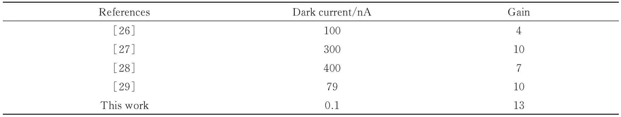
Table 2 Comparison of the dark current and gain of the theoretical InGaAs/Si APDs and experimental InGaAs/Si APDs at 95% breakdown voltage which have been reported previously
3 Conclusion
We report a novel wafer-bonded InGaAs/Si APD fabricated by SIB technique in theory.The a-SiGe material with different bandgap(different Ge content)is served as the bonding layer.The effect of the bandgap of the a-SiGe layer on the performance of the APD is studied detailedly.Due to the charge blocking effect at the bonded interface,extremely low dark current of 10-10A@ 95% breakdown voltage of the APD is achieved.In addition,the dark and optical current separate at near breakdown voltage,leaving an obvious current gap,which is beneficial to the decrease of the noise.The 3 dB-bandwidth of the device decreases with the increase in the bandgap.High gain of 30 and GBP of 60 GHz of the InGaAs/Si APD is achieved,which is close to that of InGaAs/InP APD.