Second harmonic generation from precise diamond blade diced ridge waveguides
2022-09-24HuiXu徐慧ZiqiLi李子琦ChiPang逄驰RangLi李让GenglinLi李庚霖ShAkhmadalievShengqiangZhou周生强QingmingLu路庆明YuechenJia贾曰辰andFengChen陈峰
Hui Xu(徐慧) Ziqi Li(李子琦) Chi Pang(逄驰) Rang Li(李让) Genglin Li(李庚霖) Sh. AkhmadalievShengqiang Zhou(周生强) Qingming Lu(路庆明) Yuechen Jia(贾曰辰) and Feng Chen(陈峰)
1School of Physics,State Key Laboratory of Crystal Materials,Shandong University,Jinan 250100,China
2Division of Physics and Applied Physics,School of Physical and Mathematical Sciences,Nanyang Technological University,Singapore 637371,Singapore
3Institute of Ion Beam and Materials Research,Helmholtz-Zentrum Dresden-Rossendorf,Dresden 01314,Germany
4School of Chemistry and Chemical Engineering,Shandong University,Jinan 250100,China
Keywords: optical waveguides,Nd:GdCOB crystal,second harmonic generation
1. Introduction
Optical waveguides, as one of the essential components of integrated photonics, can confine light fields in extremely small volumes.[1,2]As a result, the light intensity obtained from the waveguide volume is much higher than that in the bulk.[3-5]This feature provides meaningful advantages in nonlinear optical applications, where various nonlinear phenomena can be generated from the waveguide structure at a relatively low optical power. For example, frequency conversion processes based on waveguides feature higher conversion efficiencies and more flexible mode selection compared with those based on bulks.[4]Combining the versatility of multifunctional crystals with the compact geometries of waveguide structures, crystalline waveguides can be used to construct multifunctional optical devices with small footprints,such as on-chip lasers, compact optical modulators and nonlinear wavelength converters.[6,7]In practice,channel or ridge waveguides with light field confinement in two dimensions(2D) are preferred to one-dimensional (1D) planar waveguides due to their better optical confinement and more flexible geometry.[8]
Ion implantation, as an important method for material modification, has been applied to a variety of crystals.[9-15]By bombarding the target crystal surface with energetic ion beams, localized lattice damage and refractive index modification appear at near-surface regions, resulting in the formation of an optical waveguide.[16-18]Up to now, this technique has been applied to the preparation of waveguides in dozens of crystalline materials.[8,16]Optical waveguides manufactured by ion implantation are generally 1D planar structures. Additional surface microfabrication is therefore needed to obtain 2D waveguide structures. Of the techniques used for surface microfabrication, femtosecond laser direct writing (FsLDW) and precise diamond blade dicing are the most common. Both techniques have been utilized to manufacture ridge waveguides based on ion-irradiated Nd:YAG planar waveguides.[19-23]However,compared with the ridge waveguides fabricated by FsLDW, those prepared by precise diamond blade dicing feature lower scattering losses and a higher optical quality owing to their smoother side walls.[19,24-26]
Combining the lasing and luminescence characteristics of Nd3+ions with the nonlinear optical properties of a GdCa4O(BO3)3(GdCOB) matrix, it is shown that neodymium-doped GdCOB (Nd:GdCOB) has attractive optical properties as an excellent laser gain medium and an efficient self-frequency doubling(SFD)crystal.[27-31]In previous works, planar and channel waveguides have been fabricated in Nd:GdCOB crystals by ion irradiation[32]and FsLDW,[33]and second harmonic generation(SHG)has also been achieved using these waveguide structures. However, up to now,Nd:GdCOB ridge waveguides produced by ion irradiation and precise diamond dicing have not been reported.
In this work, we demonstrate the fabrication of Nd:GdCOB ridge waveguides by combining ion beam irradiation with precise diamond blade dicing techniques. We performed SHG at 532 nm in both ridge and planar waveguides using 1064 nm pulsed fundamental waves.
2. Experiments
The 8 at.% Nd-doped GdCOB crystal used in this work was cut to satisfy type-I phase matching conditions (θ=161.5°,φ=0°)with dimensions of 11 mm×9 mm×2.2 mm.The crystal facets of 11 mm×9 mm and 11 mm×2.2 mm were well polished to an optical grade. As Fig.1(a)shows,the surface of the sample was irradiated by carbon(C5+)ions with an energy of 15 MeV at a fluence of 2×10¹⁴ions·cm-2. As a result,a planar waveguide with a thickness of~10µm(according to the microscopic image and the ion irradiation calculations,as presented in the next section)was achieved. Ion irradiation was accomplished using the 3 MV tandem accelerator at Helmholtz-Zentrum Dresden-Rossendorf,Germany. To reduce the channel effect,the incident ion beam was deviated by 7°from the normal to the sample surface. After that,based on the planar configuration,we constructed ridge waveguides using diamond blade dicing(see Fig.1(b)). During this process,several air grooves perpendicular to the crystal surface with a size of approximately 11 mm×2.2 mm were produced with the blade (DISCO Corp., P1A851 SD3000R10B10)[34]installed on a precision dicing machine(Jingchuang Advanced,AR3000). The rotation and movement velocities were set to 20000 rpm and 0.05 mm·s-1, respectively. With vertical optical confinement provided by the ion-induced change in refractive index and lateral optical confinement offered by two neighboring grooves,ridge waveguides with widths of 10µm(WG1), 20 µm (WG2), 25 µm (WG3), and 30 µm (WG4)were formed. Both irradiation and precise diamond blade dicing are high-precision and repeatable waveguide construction techniques,[35-37]so that the waveguides are constructed with good stability.

Fig. 1. Schematic illustrations of (a) 15 MeV C5+ ion irradiation and (b)precise diamond blade dicing for Nd:GdCOB ridge waveguide fabrication.
After fabrication, micro-Raman measurements were carried out using a spectrometer (Horiba/Jobin Yvon HR800)to investigate the microstructural modification of Nd:GdCOB crystal. With a detected range of 50 cm-1-1500 cm-1,a laser beam at 473 nm was focused on the waveguide cross sections and bulk at room temperature.
Micro-second harmonic(µ-SH)spectroscopic analysis of the sample was performed to evaluate the nonlinear properties of the waveguides using a confocal microscopy testing platform. A laser beam(with a pulse duration of~20 ns,a pulse energy of~2 µJ and a pulse repetition rate of~5 MHz) at 1030 nm produced by a microjoule ultrafast fiber laser system (ANTAUS-10W-2u/5M) was coupled to the sample with a 100× objective [numerical aperture (NA)=0.3]. The reflected µ-SH signal was collected by the same objective, and after passing through several mirrors and lenses the signal was detected by a spectrometer.
As shown in Fig. 2(a), we performed SHG characterization experiments based on an end-face coupling arrangement.After the 1064 nm light beam was emitted from the pulsed laser (with a pulse width of~11.05 ns, a pulse energy of~80µJ and a repetition rate of~5 kHz),its power and polarization were adjusted by a neutral density filter and a half-wave plate, respectively. A microscope objective(25×, NA=0.4)was used for optical in-coupling. The SHG and residual fundamental signal outputs from the waveguides were collected by another microscope objective. In order to detect the SHG signal, we used a spectrometer and a powermeter behind an optical low-pass filter,which has a transmittance of~98%at 532 nm and a reflectivity of>99%at 1064 nm. Figures 2(b)-2(e)present the fundamental modes along transverse magnetic(TM)and second harmonic(SH)modes along transverse electric(TE)directions in planar and WG3 ridge waveguides(all the ridge waveguides show similar modal distributions). Both fundamental and SH waves are well confined in the waveguiding regions, showing nearly single-mode profiles, which are very beneficial for SHG.

Fig. 2. (a) The end-face coupling arrangement for SHG characterization of Nd:GdCOB waveguides. The mode field distribution of planar and WG3 ridge waveguides at 1064 nm[(b),(d)]and at 532 nm[(c),(e)](OLPF,optical low-pass filter).
3. Results and discussion
The nuclear(Sn)and electronic(Se)stopping power profiles of 15 MeV C5+ions in Nd:GdOCB were calculated using the SRIM-2008(Stopping and Range of Ions in Matter 2008)code, and the results are shown in Fig. 3(a). A non-zeroSeis observed within the ion penetration range of 0µm-10µm,peaking at approximately 1.7 keV·nm-1with a depth value of~6.7 µm. In contrast, theSnvalue remains zero within the first 9 µm below the surface and reaches a maximum of 0.16 keV·nm-1around 10 µm beneath the surface. Therefore,the electronic damage is considered to be the main cause for the change in refractive index in the ion-irradiated area,whereas the nuclear damage at the end of the ion trajectory is responsible for the creation of the optical barrier. Moreover,the formation of the waveguide layer is a collective effect of bothSnandSe. The maximum modification of refractive index in the waveguide region is about 0.003 estimated by the formula

whereΘmis the maximum incident angle at which the laser beam cannot be focused into the waveguide by the microscope objective andn=1.7184 is the refractive index of the Nd:GdCOB crystal.[32]Therefore, taking the stopping power profiles as references, we reconstructed the refractive index distribution(see Fig.3(a)). Figures 3(b)and 3(e)demonstrate the microscopic images of the planar waveguide and the WG2 ridge waveguide, respectively. The thickness of the modified layer is observed to be around 10µm,which is in fairly good agreement with the calculation performed using the SRIM-2008 code.[38]We imported the index profile into Rsoft Beam PROP 8.0[39]and simulated the near-field modal distribution.Taking a planar waveguide and WG2 ridge waveguide as examples, figures 3(c) and 3(f) display the simulated near-field distributions at 1064 nm,which are very similar to the experimental results imaged by a CCD camera in the end-face coupling setup (see Figs. 3(d) and 3(g)), suggesting the reasonability of the reconstructed refractive index profile.
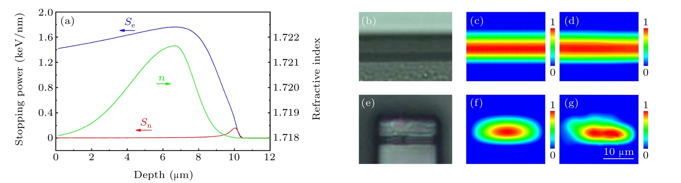
Fig.3. (a)The curves of the electronic stopping power(blue line)and the nuclear stopping power(red line)distribution,as well as the refractive index profile of the waveguide(green line),as functions of the depth. Parts(b)and(e)show microscopic images of the cross sections of planar and WG2 ridge waveguides,respectively.Experimental[(c),(f)]and simulation[(d),(g)]results of the modal profiles of planar and WG2 ridge waveguides along the TE direction at 1064 nm.

Fig.4. Output power of(a)planar and(b)WG3 ridge waveguides as a function of all-angle 1064 nm laser transmission with a constant launched power of 17.4 mW under continuous wave configuration.
To investigate the polarization-dependent properties of the waveguides, the all-angle optical transmission of the fabricated waveguide at 1064 nm was measured. As one can see from Fig. 4, for both planar and WG3 ridge waveguides (all the ridge waveguides show similar results), the output power reaches its maxima(0.86 mW and 0.62 mW)along TE polarization(0°and 180°)while decreasing to its minima(0.22 mW and 0.16 mW) along TM polarization (90°and 270°). However,the SHG process occurs under a TMω →TE2ωprocess in Nd:GdCOB waveguides, so the polarization-dependent effect has a negative impact on the frequency-doubled output power and conversion efficiency of SHG.

Fig.5. Micro-Raman spectra obtained from the WG3 ridge waveguide(red dotted line)and the bulk(blue line)of the Nd:GdCOB crystal.

Fig. 6. (a) The emitted intensity of µ-SH spectra when the laser beam (at 1030 nm) is focused at the WG3 ridge waveguide (red line), the planar waveguide (green line) and the bulk (gray line). (b) The laser spectra of the fundamental beam at 1064 nm(red line)and second harmonic generation at 532 nm(green line)in the WG3 ridge waveguide.
Micro-Raman spectra of Nd:GdCOB at the substrate and C5+ion implantation regions are presented in Fig.5. The Raman peak number and position show no differences between the bulk and waveguide areas. However,the Raman intensity in the waveguide increases with respect to the bulk,which may be a result of the lattice expansion attributed to electronic collisions during ion irradiation.[40-42]It is also possible that C5+ion implantation has caused more point defects in the crystal,leading to a slight broadening of the Raman peak half-width.
Theµ-SH responses of the ridge and planar waveguides,as well as the bulk area, were investigated, as shown in Fig. 6(a). From the SH intensity profiles, the intensity distributions for the bulk,planar and ridge waveguides have similar shapes,with their peaks at the same position.However,the SH signal in the WG3 ridge waveguide(all the ridge waveguides show similar results) is enhanced significantly, at around ten times greater than that in the bulk. It is evident that the nonlinear properties of the Nd:GdCOB crystal are well retained and further greatly enhanced in the waveguide. As shown in Fig. 6(b), the spectra measured by the pulsed laser pump of the fundamental(at 1064 nm)and SH(at 532 nm)waves from the WG3 ridge waveguide clearly depict the nonlinear process of SHG in Nd:GdCOB waveguides. The 1064 nm fundamental and SH waves are determined to be TM-and TE-polarized,respectively. This verifies that the SHG process occurs under the TMω →TE2ωprocess,which is in good accordance with the phase matching configuration of the bulk.
Figure 7 illustrates the second harmonic powers (average power)and the conversion efficiencies as functions of the 1064 nm fundamental pump power for planar and WG4 ridge waveguides (WG4 has the best frequency doubling performance of any of the ridge waveguides)under the pulsed configuration. The measured data points are marked with solid circles (blue for the SH powers and red for the conversion efficiencies). For the planar waveguide, the maximum average power output of the SH light is~1.04 mW with a pump power of~112 mW, resulting in a conversion efficiency ofη ≈8.32 %·W-1. The maximum average output power of the SH light for the WG4 ridge waveguide is~2.80 mW,which is around two times larger than that of the planar waveguide. The conversion efficiency reaches a maximum value of~22.36 %·W-1, leading to a significantly enhanced performance. An annealing treatment at 260°C for about 30 min was carried out in order to observe the changes in related nonlinear properties. However,this thermal operation has a negligible influence on the SHG performance of the waveguides.The data on maximum SHG output power (Pmax), the conversion efficiency (ηmax) and the propagation losses (α) for all ridge waveguides are summarized in Table 1, and the related properties of the planar waveguide are also included for reference. With an increase in the width of the ridge waveguide,the corresponding maximum SHG power and conversion efficiency will be enhanced. The similar dependence of the SHG properties on the ridge width can also be found in previously reported KTiOPO4ridge waveguides.[26]Furthermore,ridge waveguides show better performance than planar waveguides in frequency doubling, mainly due to the more compact structure of ridge waveguides, which leads to a stronger light intensity confined in a limited volume. The propagation losses of the ridge waveguides decrease with increase in ridge width. All ridge waveguides have higher propagation losses than planar waveguide,mainly due to the relatively high waveguide side-wall roughness caused by the dicing process.By optimizing the dicing parameters, such as the blade type and its rotation velocity,the roughness of the waveguide sidewall can be lowered,thereby reducing the propagation loss of the fabricated ridge waveguide.[43]In addition, reduction of the waveguide side-wall roughness can be also realized using ion beam milling.[44]The frequency doubling efficiency will be improved if waveguide losses are optimized, and a selffrequency-doubling effect can be expected.

Table 1. The maximum output SH powers(Pmax),the maximum conversion efficiencies(ηmax)and propagation losses(α)of the Nd:GdCOB planar and ridge waveguides.

Fig.7. Second harmonic power and the corresponding conversion efficiency as functions of the fundamental pump power in(a)planar and(b)WG4 ridge waveguides.
4. Conclusion
We have fabricated ridge waveguides in Nd:GdCOB crystals through a combination of carbon ion irradiation and precise diamond blade dicing. Based on an end-face coupling setup,the optical waveguiding properties of both Nd:GdCOB ridge waveguides and planar waveguide were experimentally investigated. The simulated modal profiles agree well with the measurements, suggesting the rationality of the constructed index profile based on stopping powers. From the micro-Raman spectrum, lattice expansion occurs during carbon ion implantation with more point defects.Throughµ-SH analysis,the nonlinear properties of the Nd:GdCOB crystal have been found to be fully preserved and greatly enhanced within the waveguides. SHG at 532 nm based on type I phase matching has been observed under a 1064 nm pulsed laser configuration. The maximum SH power of~2.80 mW was obtained in the WG4 ridge waveguide, and the corresponding conversion efficiency was~22.36 %·W-1. For planar waveguide,the maximum SH power was~1.04 mW with a conversion efficiency of 8.32%·W-1.Our work demonstrates that carbon ion irradiation combined with precise diamond blade dicing can be used to fabricate efficient nonlinear waveguides, providing potential applications in integrated photonics.
Acknowledgments
The authors thank Dr Y.Cheng for waveguide fabrication and Professor H.Yu forµ-SH analysis.
Project supported by the Taishan Scholars Youth Expert Program of Shandong Province and the Qilu Young Scholar Program of Shandong University,China.
猜你喜欢
杂志排行
Chinese Physics B的其它文章
- Erratum to“Accurate determination of film thickness by low-angle x-ray reflection”
- Anionic redox reaction mechanism in Na-ion batteries
- X-ray phase-sensitive microscope imaging with a grating interferometer: Theory and simulation
- Regulation of the intermittent release of giant unilamellar vesicles under osmotic pressure
- Bioinspired tactile perception platform with information encryption function
- Quantum oscillations in a hexagonal boron nitride-supported single crystalline InSb nanosheet