Monte Carlo simulation for performance evaluation of detector model with a monolithic LaBr3(Ce) crystal and SiPM array for γ radiation imaging
2022-09-16WeiLuLeiWangYongYuanTingZhangGeTangMingZheLiuXianGuoTuoJingNing
Wei Lu · Lei Wang· Yong Yuan · Ting Zhang· Ge Tang ·Ming-Zhe Liu · Xian-Guo Tuo · Jing Ning
Abstract In recent years, LaBr3(Ce) crystals and silicon photomultipliers (SiPMs) have been increasingly used in radiation imaging.This study involved the establishment of a detector model with a monolithic LaBr3(Ce) crystal and SiPM array for γ-radiation imaging on the GEANT4 platform. The optical process included in the detector model was defined by key parameters, such as the emission spectrum, scintillation yield, and intrinsic resolution of the LaBr3:5%Ce crystal, as well as the detection efficiency of the SiPM array.The response of the detector model to 57Co flooded field irradiation was simulated and evaluated. The radiation images generated by the detector model exhibited a compression effect that was very close to that on images acquired by the physical detector.The spatial resolution of the simulated detector closely approximates that of the physical experiment. A detector model without the optical process was also established for comparison with a detector using the optical process. Both were used in a near-field modified uniform redundant array (MURA) imaging system to acquire images of a point source and a ring source of 57Co at the center of the field-of-view of the imaging system. The spatial resolution and signal-to-noise ratio of the images that were reconstructed using the two detector models were determined and compared.Compared with the detector model without optical processes,although the images from the proposed detector model have slightly inferior signal-to-noise ratios and more artifacts, they are more consistent with the reconstructed versions of images acquired in real physical experiments. The results confirm that the detector model can be used to design a γ-radiation imaging detector and to develop an imaging algorithm that can significantly shorten the development time and reduce the cost.
Keywords Scintillation photons · Monte Carlo · SiPM array · Spatial resolution · Monolithic LaBr3(Ce) crystal
1 Introduction
The development of inorganic scintillators and an increasing variety of low-light sensors in recent years has enabled the widespread use of scintillator detectors in nuclear physics, particle physics, radiation imaging, and other fields. Scintillator crystals have the advantages of a high optical yield, short decay time, and high energy resolution, making them ideal crystalline materials for developing nuclear instruments. Two main types of scintillator crystals are used in γ-radiation imaging: array crystals and monolithic crystals. An imaging detector with an array crystal can achieve high spatial resolution,mainly determined by the pixel size of the crystal array. The disadvantage of this type of detector is that its energy resolution and detection efficiency are significantly reduced by the photon absorption of the reflective layer material among the crystal pixels and the thickness of the crystal array. However, detectors with monolithic crystals have the potential to provide sub-millimeter spatial resolution [1–4]and energy resolution as good as that of an array crystal. Although γ-radiation imaging systems with array crystals have long been used in systems employed by homeland security and those used for hazardous material transport, security inspections, and nuclear emergencies[5–7], in some areas, such as public safety and internal contamination imaging, radiation imaging systems are expected to not only capture information about the radiation distribution, but also about the constituent nuclides.Therefore, a γ-radiation imaging system with a monolithic crystal detector that offers both good energy and high spatial resolution, has become the preferred choice.
In the γ-radiation imaging process, the energy of an incident γ-ray is either partially or fully converted into scintillation photons by the scintillator. During the transportation of scintillation photons in the crystal, some photons are directly recorded by the photoelectric sensor array, whereas others are recorded by the array after reflection and refraction by the encapsulation material of the crystal.Thus,the transportation of scintillation photons is a key process in radiation imaging, particularly in simulation imaging studies.
In the research design of γ-ray encoded-imaging (decoding algorithm or localization algorithm), the encoding process can be approximated as a linear system model of geometrical optics owing to the high energy and short wavelengths of γ-rays, and the diffraction effect can be neglected; thus, the detector is generally reduced to a detector plane (or imaging plane). The coordinates of the points of incidence of the γ-rays on the detection plane are registered as the coordinates of the ray interaction with the detector [8–11]. Most simulation studies have focused on the energy deposition of the incident ray in the detector but ignored the complex transport and absorption processes of scintillation photons generated by the deposition energy in the crystal.
In fact,the transportation and distribution of scintillation photons are highly dominated by the thickness of the crystal, the optical properties of the crystal, and the encapsulation material, which directly affect the accuracy of the localization of the location at which an incident γray interacts with the detector [12–14].
In the actual imaging process, the detector uses a localization algorithm to determine the coordinates of the point of interaction of the rays through the optical light distribution, and uses the coordinates for image reconstruction. In previous Monte Carlo (MC) studies [1, 15],owing to the absence of an optical process, the process whereby visible light is generated and transported inside the crystal was not accurately described. Therefore, these methods did not enable the energy of deposited rays to be converted into an optical light distribution, and the simulation program only provided the coordinates of the energy deposition points as its direct output.As a result,the energy resolution of the detector could not be predicted directly,and an innovative design of the ray location and imaging algorithms could not be developed. Because the output of the detector did not reflect the statistical fluctuation of the optical photons and transport process [16, 17], the energy resolution could not be predicted directly,and the γ-energy spectrum could only be simulated by Gaussian broadening,for which the Gaussian broadening coefficients of the spectral lines had to be obtained in advance.
The geometry and tracking (GEANT4) platform,developed by CERN, provides a complete set of tools for all areas of detector simulation, including geometry,tracking, detector response, run, event and track management,visualization,and a user interface.The platform also includes a comprehensive set of physical processes to handle the diverse interactions of particles with matter over a wide energy range. For many physical processes, a selection of different models is available. The platform is thus able to accurately simulate γ-imaging [18].
This work resulted in the proposal of an accurate MC detector model with a monolithic LaBr3(Ce) crystal and SiPM array. The aim was to conduct an in-depth study of the performance of a detector equipped with a monolithic crystal, which necessitated the development of a highly efficient and convenient detector model for simulation to facilitate research in radiation imaging and advanced imaging algorithms. The simulation results were in good agreement with results reported in the literature. The detector model was employed to establish a modified uniform redundant array(MURA)radiation imaging system in GEANT4. The energy and spatial resolutions of the imaging system are evaluated and discussed.
2 Model of imaging detector
Three basic steps were used to set up the model of the detector in GEANT4. The first step entailed the establishment of a geometric model of the detector and specification of the properties of the materials and relative geometric positions of each component of the detector. The second step involved the selection of an appropriate physical process, which is related to the energy deposition of the gamma rays in the detector and emitting scintillation. The third step was to locate the interaction point. The coordinates of the interaction points of the incident ray can be calculated based on the scintillation light distribution represented by the output of the SiPM array.
2.1 Detector model
Figure 1 shows the structure of the imaging detector. A square LaBr3(Ce)crystal(51 mm × 51 mm × 5 mm)was used as the scintillator, which was covered by Teflon foil(thickness 0.3 mm) as the diffuse reflective layer in the front. The scintillator was surrounded and encapsulated by aluminum foil(thickness 0.5 mm)as the specular reflective layer. A glass layer (thickness 3 mm, reflectivity 1.5) and optical grease (thickness 0.1 mm, reflectivity 1.41) was positioned between the bottom of the crystal and SiPM array.The SiPM(Micro-30035-TSV of ONSEMI)consists of a 16 × 16 array, with a sensitive area of 3.07 × 3.07 mm2and package area of 3.16 × 3.16 mm2.
2.2 Physical processes
The physical processes of the MC detector model with monolithic LaBr3(Ce) crystals and the SiPM array proposed in this paper mainly include electromagnetic interactions and optical photon processes. The electromagnetic interactions between the γ-rays and charged particles in the detector model mainly include the photoelectric effect,Compton scattering, pair production, ionization, bremsstrahlung, and multiple scattering. The optical photon processes within the detector model mainly include scintillation, Cherenkov radiation, Rayleigh scattering, Mie scattering, bulk absorption, refraction, reflection [specular spike(SS),specular lobe(SL),Lambertian(L),backscatter(BS)], and boundary processes. The scintillation photons incident on the SiPM array are absorbed by the metal surface of the SiPM and converted into electron–hole pairs according to the photon detection efficiency (PDE) of the SiPM. The avalanche processes in the SiPM are not included in the simulation.
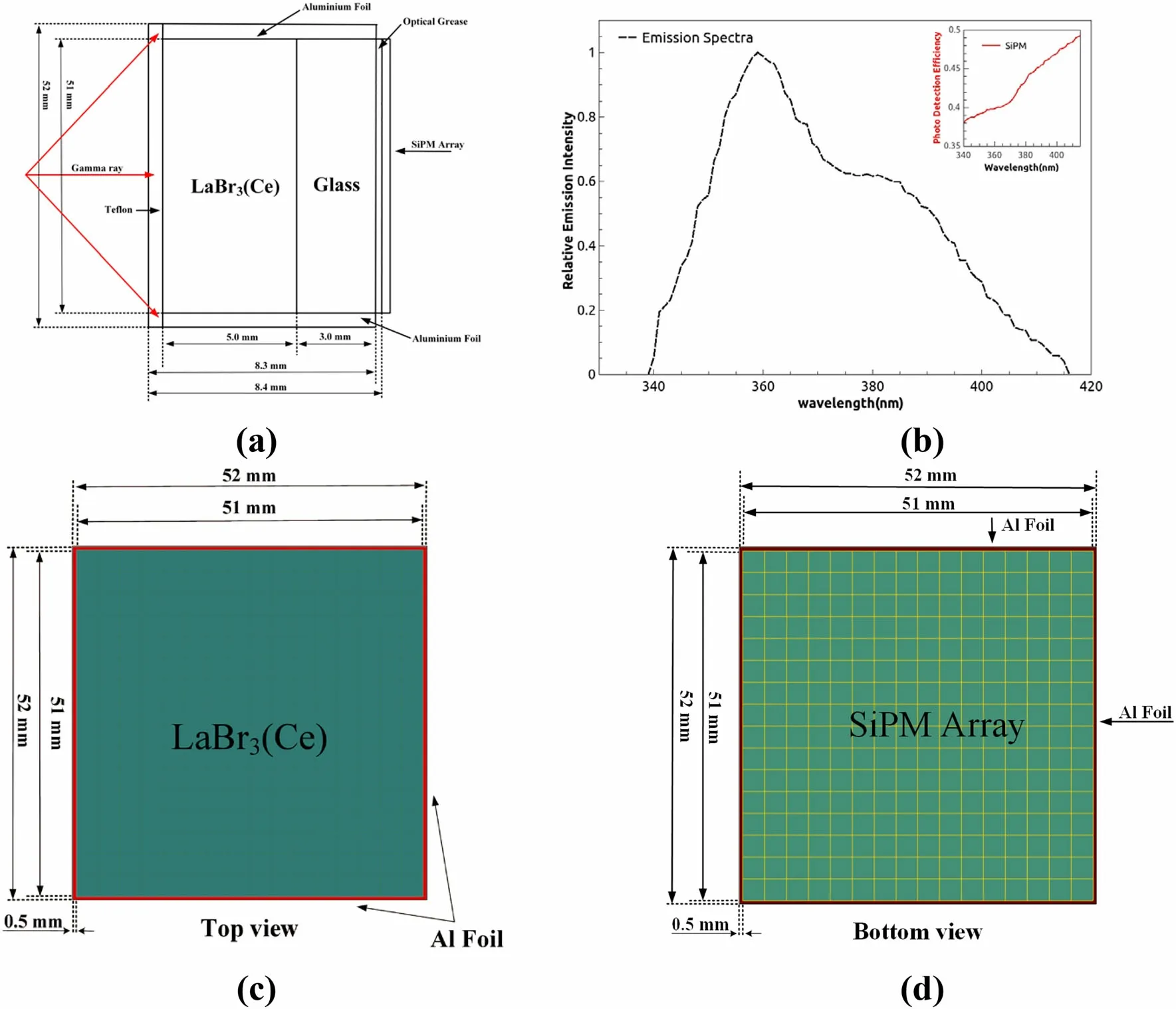
Fig.1 (Color online)a Structure of the Monte Carlo detector model with monolithic LaBr3(Ce)crystal and SiPM array.b Emission spectrum of the LaBr3(Ce) crystal in GEANT4. c Top and d bottom views of the structure
The most important feature of the LaBr3(Ce)detector is that the crystal contains138La and227Ac, making its background energy spectrum different from the natural background spectrum in the environment. In the low-energy region (0–1800 keV), the background spectrum mainly arose from the gamma leap of138La (789 and 1436 keV).When simulating the background spectrum,we calculated the activity of the crystal according to the volume of the crystal and randomly distributed138La in the crystal(the activity of138La in the crystal is 1.428 Bq/cm3[19], and the total activity of138La in the crystal is 18.6 Bq). Because of the small size of the crystal, it has a low stopping power for 789 keV and 1436 keV γ-rays,which means its effect on the imaging results is negligible.In the high-energy region (1800–2800 keV), the rays mainly originate from227Ac and the environmental background. Because of the small number of counts, they have little influence on the energy spectrum measurement;therefore, they are not considered in the detector.
2.3 Parameters of the LaBr3(Ce) crystal model
The main parameters of lanthanum bromide crystals include the emission spectrum of the crystal, decay time constant, intrinsic resolution, crystal refractive index, and light yield. The emission spectra of LaBr3(Ce) crystals varied depending on the Ce content. An increase in the Ce concentration caused the light yield to change slightly, but the decay time decreased. Generally, the decay time constant contains a FAST TIME CONSTANT and a SLOW TIME CONSTANT. Because the fast decay component of the decay time constant of the LaBr3: 5% Ce crystal reached 97%, the decay time constant was set to include only the fast component. The FAST TIME CONSTANT was set to 15 ns,and the value of YIELDRATIO was set to 1 [20, 21]. The light yield (SCINTILLATION YIELD,SCY) of the crystal was set to 63,000/MeV and the refractive index of the crystal was set to 1.85 [21]. In GEANT4, the emission spectra acquired from physical experiments [22]are used to establish the emission spectra of the crystal model. In G4Step, the scintillation photons produced during the γ-interaction event are tracked, and the photons are counted by energy to obtain the crystal emission spectrum, as shown in Fig. 1b, which is consistent with the emission spectrum in the literature [22].
Among the parameters used to simulate the optical process of the crystal,RESOLUTION SCALE(RES)plays an important role and directly represents the intrinsic resolution of the crystal, which generally broadens the statistical distribution of the generated photons. The wider intrinsic resolution is due to impurities that are typical for doped crystals such as NaI(Tl) and CsI(Tl). The RES was determined using M and δ.

Because the Ri(intrinsic resolutions) of the LaBr3(Ce)crystal for γ-rays at 662, 122, and 59 keV were 2.81%,5.02%, 7.0%, respectively [21], according to Eq. (1), the RES of the LaBr3(Ce)crystal in the detector model at 662,122,and 59 keV were calculated to be 2.43,1.86,and 1.78,respectively.
Based on the above steps, the parameters of the LaBr3(Ce)crystal model in GEANT4 were determined and are listed in Table 1.
The surface model between the LaBr3(Ce) crystal and aluminum foil was specified as a UNIFIED model,and the surface type was set to be dielectric-dielectric. Because of the thin layer of air between the LaBr3(Ce) crystal and encapsulation material, a ground-back-painted (GBP)coating was employed to describe this layer. The Finish parameter was set to ground, and the sigma alpha parameter was set to 1°. The reflectivity (R) of the LaBr3(Ce)crystal was set to 97%, with 94% for specular lobe reflection (SL), 3% for specular spike (SS), and 3% for Lambertian reflection(L)in the reflection component[13].Scintillation photons are reflected, refracted, or absorbed among the surfaces.
The surface model between LaBr3(Ce) and Teflon was also set to UNIFIED, and the surface type was set to dielectric-dielectric. The dielectric materials were separated by a GBP coating with 95% specular lobe reflection(SL) and 5% Lambertian reflection (L). The impact of the reflectivity was investigated by setting R = 0.98 and σα-= 3.44° for the surface finish. The surface model of the SiPM was defined as a dielectric-metal surface, with detection efficiency of 1 and R = 0, indicating that all photons were absorbed, with any reflection and refraction.
2.4 Photoelectric conversion
The photon detection efficiency(PDE)Epdeof the SiPM[23] is defined as:

where Eqeis the quantum efficiency (QE) of the corresponding energy of the SiPM, which is the probability of the absorption of a photon by the avalanche photodiode(APD) to produce an electron–hole pair; Dfis the geometric filling factor,which is the area ratio of the APD areato the entire SiPM region in the SiPM;Pgis the probability of the electron–hole pair producing a Geiger avalanche.The Epdeof the SiPM for the wavelength range of 340–415 nm is shown in Fig. 1b.

Table 1 Scintillation characteristics of LaBr3(Ce) crystals
When the incident γ-rays interact with the crystal and deposit energy in the crystal, the simulation program produces a corresponding number of isotropic scintillation photons at the interaction position according to the values of SCY, RES, and the deposition energy. The total reflection, refraction, or reflection effect of the scintillation photons that are transported to the boundary between the crystal and the encapsulating material (aluminum foil or Teflon) is simulated according to the wavelength and incident angle of the photon and the refraction coefficient of the material on both sides of the boundary.Scintillation photons that are transported to the boundary between the optical grease and SiPM can either be absorbed by the metal surface of the SiPM array or reflected back into the LaBr3(Ce) crystal. When an optical photon is absorbed by the SiPM,the simulation program converts the scintillation photon into an electron–hole pair according to the Epdeof the SiPM. After reflection or refraction of the scintillation photons by the encapsulating material, some photons are absorbed by the crystal attenuation,and others are absorbed by the SiPM array and converted into electron–hole pairs.
3 Simulation results and discussion
3.1 Detector response to flood-field irradiation
The response output area (ROA) of the monolithic LaBr3(Ce)crystal detector model was validated by using it in an MC flood-field irradiation experimental simulation corresponding to reported experiments [24]. In the simulation, a flood-field and collimated57Co source emitting 122 keV rays was used to irradiate the monolithic LaBr3(Ce) crystal detector model. The SiPM array in the detector model was configured as a 64-pixel array (8 × 8 pixels, 6 mm pixels).
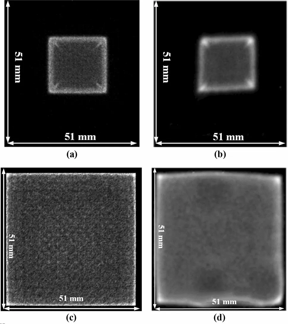
Fig. 2 57Co source flood-field irradiation experiment: a simulated and b experimental images[24],respectively.ROA of the c simulated image for the TCOG method and d experimental image in the literature [24]
Figure 2a shows a simulated image of the flood-field irradiation acquired by the monolithic LaBr3(Ce) crystal detector model proposed in this paper.Figure 2b shows an image of the irradiation recorded in a physical experiment[24].In Fig. 2a,because of the image shrinkage effect, the ROA was compressed to form a square from the surroundings to the center, and counts in the central region were uniform, whereas counts at the boundary were significantly higher than those at the center. The image shrinkage effect is related to the accuracy of the ray incidence locations registered by the imaging system. A comparison of Fig. 2a,b reveals that the simulated images are consistent with the physical experimental image, indicating that the physical processes in the detector model,especially the physical processes of scintillation photon generation, transmission, reflection, refraction, and absorption, closely resembled the real response of the physical detector to γ-irradiation.
The truncated center-of-gravity (TCOG) [25] algorithm is often used to suppress noise and reduce image shrinkage.
The TCOG algorithm uses each row (or column) in the SiPM array as one channel,calculates the sum of the signal of each channel,and sets a threshold according to the total signal. The signals below the threshold in the SiPM array were excluded, and signals above the threshold were included in the localization operation as valid signals.
We used TCOG to estimate the ray incidence location using the scintillation photon distribution collected by the SiPM array. According to Fig. 2a, b, although the ROA was improved and the shrinkage effect significantly reduced, the efficiency by shrinkage still existed at the edges of the reconstructed image, as shown in Fig. 2c, d.
Figure 2c, d shows that the linearity of the simulation results is more pronounced than that of the experimental results.This is mainly caused by the non-uniformity of the light guide and the inconsistency of the response of the SiPM,etc.,in the physical experiments.Both the simulated and experimental images exhibited similar high counting phenomena on the vertices and the shrinkage effect at the edges, which indicates that the optical photon processes in the detector model were highly consistent with those of the physical imaging system.
3.2 Intrinsic spatial and energy resolution
To test the intrinsic spatial resolution of the imaging detector model, we used a parallel-beam (PB) collimator model coupled with the imaging detector model to set up a PB imaging system in GEANT4,according to the literature[26]. The MC imaging system is shown in Fig. 3.
A lead PB collimator with 1-mm-diameter holes spaced 5 mm apart was used to evaluate the spatial resolution.Figure 4a shows that the collimated aperture image has a clear outline; however, owing to the shrinkage effect, the image of the apertures close to the boundaries is slightly distorted.Both Fig. 4a,b show very similar edge distortions and high counts at the center. This indicates that the simulated images are in good agreement with the images acquired in physical experiments,as reported in the literature[26].
The spatial images of the 20 holes in the fourth row and fourth column acquired by the imaging system with the parallel-beam collimator are shown in Fig. 4c. The spatial resolution in the fourth row is in the range 0.62–1.1 mm with an average value of 0.89 mm. The spatial resolution of the fourth column is in the range 0.66–1.1 mm with an average value of 0.93 mm. The spatial resolution determined in the physical experiments was in the range 1.03–1.32 mm with an average value of 1.13 mm[26].The spatial resolution of the simulated detector therefore closely approximated that of the physical detector.
Because the simulated detector does not consider the statistical fluctuations caused by the electronic circuit, the spatial resolution of this detector is slightly lower than that of the physical detector.
The energy resolution (R) of the full energy peak measured with the scintillator coupled to the SiPM array can be expressed by Eq. (3) [27]

· In Eq. (3), δinis the intrinsic resolution due to the fluctuation of the number of optical photons during the scintillation. The intrinsic resolution of crystals is related to many factors, such as the variation of local light output because of the inhomogeneity of crystals,inhomogeneous reflectivity of scintillator reflectors,and non-uniform response of crystals to energy deposition.
δpis the transfer resolution, which is the deviation caused by the transport of optical photons from the crystal generation to the absorption by the SiPM array. In scintillator detectors, the transfer resolution is negligible compared with the other components of the energy resolution.
δnis the dark noise contribution.
δstis the statistical contribution of SiPM.
δstis defined as Eq. (4).
where F is the excess noise factor,with a typical value of 2 for εAPD[27], and N is the number of electron–hole pairs generated by the absorbed scintillation photons of the SiPM.
In G4StepAction, the number of scintillation photons and electron–hole pairs in each gamma event were registered to obtain the intrinsic energy resolution of the crystal(Rint) and the energy resolution (Rd1) of the simulated detector.

Fig.3 (Color online)Imaging system with the parallel-beam collimator model and the monolithic LaBr3(Ce)crystal imaging detector model in GEANT4. a Top view, b right side view, and c bottom view of the imaging system
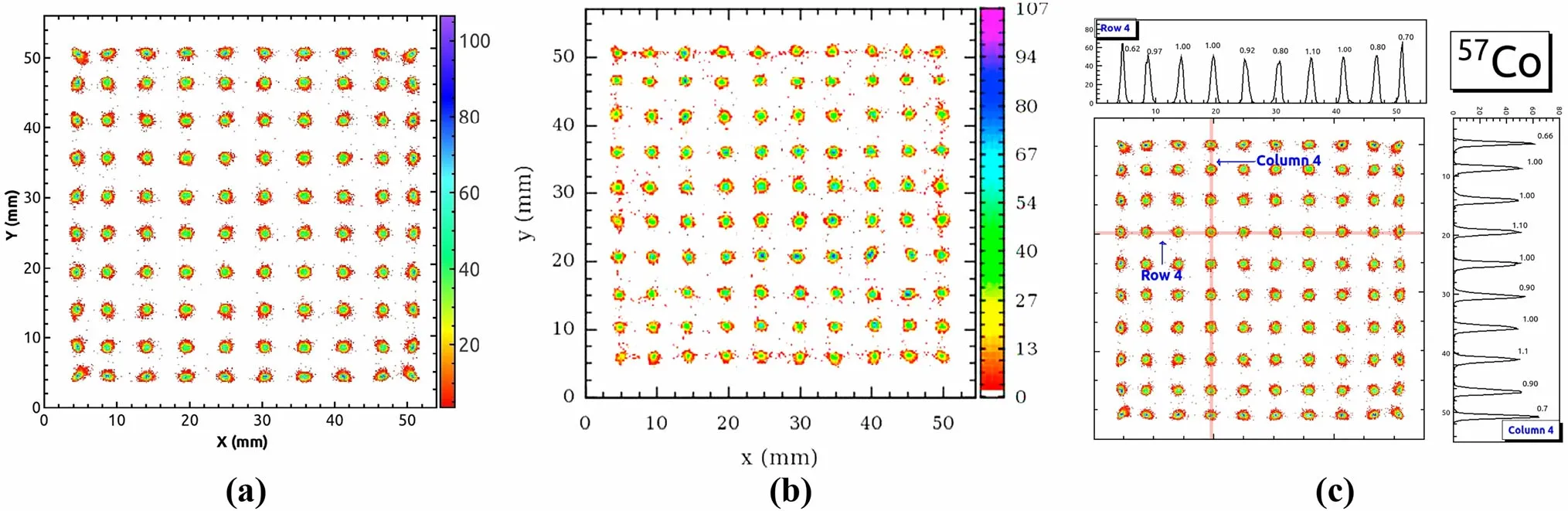
Fig. 4 (Color online) Reconstructed image acquired by the imaging system with the parallel-beam collimator under 57Co source irradiation: a Monte Carlo simulation image acquired by the imaging detector model, b experimental image from the literature. c Intrinsic spatial resolution of the Monte Carlo simulation image acquired by the imaging system with the parallel-beam collimator under 57Co source irradiation
The γ-ray energy spectra obtained by the simulated detector at 122 and 59 keV are shown in Fig. 5.
In Fig. 5,a(1)and b(1)are the photon spectra of57Co and241Am sources, respectively. Because the number of electron–hole pairs is proportional to the amplitude of the SiPM output pulse,the detector response spectrum was obtained by counting the number of electron–hole pairs output from the SiPM array,as shown in Fig. 5(a2)and b(2).
Because the simulation program does not simulate the dark noise and the contributions of δstand δnto the energy resolution,the energy resolutions of the simulated detector for γ-rays at 122 keV and 59 keV are 6.47 ± 0.36% and 10.49 ± 0.38%, respectively, which are an improvement relative to 9.78% and 16.09%, respectively. After δstwas added to the resolution according to Eq. (4), the corrected energy resolutions of the simulated detector (Rd2) were 9.57 ± 0.27% and 15.33 ± 0.29%, respectively (Table 2).The parameters of Rd2were calculated using Eq. (5),where F is the excess noise factor with a typical value of 2,and N is the number of electron–hole pairs in each simulation experiment.

Because the effect of dark noise δnis not considered,the energy resolution of the detector model is slightly lower than, but very close to, that of the physical detector.

Fig. 5 Energy resolution of the simulated detector. a(1): Photon spectrum generated inside the crystal (57Co). a(2): Energy spectrum from the detector model (57Co). b(1): Photon spectrum generated inside the crystal (241Am). b(2): Energy spectrum from the detector model (241Am)

Table 2 Resolution of the simulated and experimental detectors
3.3 Simulation of MURA coded aperture imaging
A MURA coded aperture collimator model and an imaging detector model with an optical process (detector model A) were employed to set up the MURA coded aperture imaging system in GEANT4, as shown in Fig. 6a[1]. The collimator measured 72.7 mm × 72.7 mm × 2 mm.The SiPM array was a 256-pixel array(3 mm pixels).For comparison with detector model A, we built another imaging detector model without the optical process (detector model B),as shown in Fig. 6b.In detector model B,the detection surface was divided into 280 × 280 = 78,400 small windows.An incident ray on the detector was located according to the incident window. The radioactive source emitted isotropic 122 keV γ-photons at a distance of 150 mm from the collimator and 200 mm from the detector surface. The source, collimator, and detection planes were parallel and coaxial to each other.
The57Co point source was placed at the center of the radioactive source plane (0, 0). The source emitted 1 × 10¹⁰isotropic γ-rays to obtain the projected image of the MURA coded aperture collimator, as shown in Fig. 7(a1) and (b1). The maximum likelihood-expectation maximization (MELM) algorithm was then employed to reconstruct the image of the point source, as shown in Fig. 7(a2) and (b2).
According to Fig. 7(a1), the TCOG algorithm was used in imaging system A to localize the ray interaction position, which leads to a reduction in ROA and distortion of the edge projection. As shown in Fig. 7(b1), imaging system B directly records the incident coordinates of photons without an optical process. Therefore, distortion of the light-field and shrinkage effect did not occur, and a very clear projection image was acquired.
The theoretical resolution of the γ-camera is expressed by Eq. (6) [28]:

Fig. 6 (Color online) MURA imaging system in GEANT4.a Imaging system A with detector model A. b Imaging system B with detector model B

As is clear from Fig. 7(a2) and (b2), the spatial resolution of imaging system A is worse than that of imaging system B.The theoretical resolution(R)of imaging system A was designed to be 1.95 mm [28]. The FWHM of the point source was 5.2 pixels, and the system resolution of imaging system A was 2.13 mm. The error of the simulation resolution relative to the theoretical resolution was 9.2%. The spatial theoretical resolution of imaging system B was 1.73 mm, and the spatial resolution of imaging system B was 1.82 mm, with a relative error of 5.7%.
The difference is attributed to the statistical fluctuation in the scintillation process in detector model A, ranging from generation to absorption by the SiPM array, which expands the spatial resolution of the imaging system. On the other hand, the projected image acquired by imaging system A presents the shrinkage effect, as in the physical experiment [24], making the imaging process more realistic. In imaging system B, the detector model did not include the process whereby the scintillation light is transported in the crystal, and the localization of the position at which the incident ray interacted with the crystal was idealized. This obviates the need to locate the interaction position using algorithms such as the TCOG and avoids the localization error caused by the distortion of the light field.
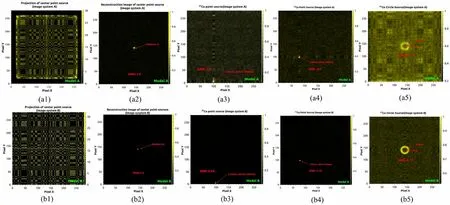
Fig. 7 (Color online) (a1) and (b1) Projection of the MURA collimator at the detector plane under irradiation of the 57Co point source: (a2) and (b2)Reconstructed images of the 57Co point source.Reconstructed images of point source located at(a3)–(b3)(- 20 mm,- 65 mm, 160 mm) and (a4)–(b4) (- 30 mm, - 20 mm, 160 mm).(a5)–(b5) Reconstructed images of the circular source with outer and inner diameters of 8 mm and 5 mm,respectively, at the center of the field-of-view (FOV)
Detector models A and B were employed to image two57Co point sources and57Co circular sources in GEANT4.In the simulation, the two point sources were located at(- 30 mm, - 20 mm, and 160 mm) and (- 20 mm,- 65 mm, and 160 mm), respectively, and the number of gamma photons was 3×10⁶. The circular source had an inner diameter of 5 mm, outer diameter of 8 mm, circular thickness of 3 mm,and the number of gamma photons was 3×10⁸.
As shown in Fig. 7 ((a3,b3), (a4,b4), and (a5,b5)), the MC imaging system accurately reconstructed the position and shape of the radiation source. A comparison of the three groups of reconstructed images reveals that the reconstructed image quality from imaging system B is superior to that from imaging system A. This is evident from the presence of greater amounts of noise and stronger artifacts in Fig. 7 (a3), (a4), and (a5) obtained by imaging system A.
When the radiation source is located at the edge of the FOV, the rays are more incident on the edge of the detector. In this situation, the scintillation photons generated in detector model A interact with the reflective layer at the edge of the detector, and the light-field distribution appears distorted, with a strong edge enhancement and shrinkage effect. Therefore, the interaction point of the incident γ-ray located by the TCOG algorithm is strongly influenced by the light-field distribution, which leads to compression and artifacts in the reconstructed image. This is consistent with the physical imaging system.
The idealized grid localization used imaging system B and ignored the scintillation photon transport in detector model B. Although this helped to ensure highly accurate localization and excellent image quality, the idealized approach deviated from the physical imaging system.Because of the accurate optical processes in detector model A,the electron–hole pair distribution it produced as output is a more realistic representation of the response of the physical detector, and can effectively guide the design of physical imaging systems and related algorithm development.
3.4 Using the detector model to design an imaging system
In a coded γ-ray imaging system (e.g., MURA), the main performance parameters of the system are determined by the coding and detector systems. The encoded imaging system is designed by simplifying the detector and collimator to the image and collimation planes, respectively,and the field-of-view(FOV)parameters are designed on the basis of the geometric position and size of the collimator and detector [9]. In a γ-ray imaging system, the point at which the ray interacts is localized by the relevant localization algorithm, mainly by using the light distribution data output received from the sensor [3]. The detector model proposed in this paper can accurately output the scintillation light distribution of the detector; thus, the accuracy of the localization algorithm can be verified, and a new localization algorithm can be developed.
4 Conclusion
This study established a detector model with a monolithic LaBr3(Ce) crystal and SiPM array for γ-radiation imaging on the GEANT4 platform. The main components of the detector model was a 5-mm-thick LaBr3(Ce)monolithic crystal encapsulated in aluminum foil, Teflon,and a SiPM array. The process according to which scintillation photons are transported inside the scintillator detector was comprehensively considered. The detector model had an energy resolution of 15.33 ± 0.29% at 59 keV and 9.57 ± 0.27% at 122 keV. The intrinsic resolution of 0.93 mm of the imaging detector model closely approximated the value of 1.13 mm reported in the literature. The MURA imaging system based on the imaging detector model with the optical process also provided realistic images of both the57Co point and ring sources,with noticeable edge enhancement and shrinkage effects,in agreement with the physical experiments.
The detector model proposed in this study is expected to be useful for the performance evaluation of γ-cameras by significantly reducing the time and cost of developing the instrument.The advantage of the detector model is that the physical and optical processes in the imaging process are considered in detail; thus, the imaging results are highly consistent with the physical experimental results. The disadvantage is that the inconsistency of the detection efficiency of the SiPM array and the scintillation efficiency inside the crystal are not considered; consequently, the uniformity of the simulation results is higher than that of the physical experimental results. This paper presents the first comparison of the imaging results between optical and non-optical models. Our findings showed that the imaging results of the optical model have practical significance and can serve to guide the research design of a detector more accurately.
Author contributions All authors contributed to the study conception and design. Material preparation, data collection and analysis were performed by Lei Wang,Wei Lu,and Yong Yuan.The first draft of the manuscript was written by Wei Lu and all authors commented on previous versions of the manuscript.All authors read and approved the final manuscript.
杂志排行

Nuclear Science and Techniques的其它文章
- Transient analysis and optimization of passive residual heat removal heat exchanger in advanced nuclear power plant
- Recent progress in two-proton radioactivity
- Selection diagram of design algorithms for neutron-focusing supermirrors
- Flow field effect of delayed neutron precursors in liquid-fueled molten salt reactors
- A high fidelity general purpose 3-D Monte Carlo particle transport program JMCT3.0
- New flexible CsPbBr3-based scintillator for X-ray tomography