A Current Mode Low⁃Noise Gm⁃C Filter with a Cut⁃Off Frequency of 5 GHz in Telecommunication System
2022-09-15,
,
1.School of Information Science and Engineering,Southeast University,Nanjing 210096,P.R.China;
2.National Mobile Communication Research Laboratory,Southeast University,Nanjing 210096,P.R.China;
3.Purple Mountain Laboratories,Nanjing 210096,P.R.China
Abstract: The high linearity low-noise filter is an indispensable key circuit in the communication system.Based on the structure of current-reuse source-degradation operational transconductance amplifier(OTA),a 5 GHz current-mode low-noise Gm-C filter suitable for high-speed communication systems is proposed.Thanks to the proposed current mode structure and the OTA’s high-power efficiency and high linearity,the filter obtains good noise and high linearity performance with very low power consumption.The filter is designed in standard 65 nm CMOS technology and occupies a core area of 0.06 mm².The simulation results show that the operating bandwidth is 5 GHz,the IIP3 is 35 dBm,and the power consumption is only 3.2 mW.
Key words:Gm-C filter;lowpass filter;current mode filter
0 Introduction
Modern wireless telecommunication systems evolve towards broadband features with high filter⁃ing requirements for in-band and out-band blockers.Normally,out-band blockers are filtered out by offchip surface acoustic wave(SAW)filters.The inband blockers need to be filtered by an integrated fil⁃ter when the RF signal is down converted to the baseband[1].In direct conversion receivers with very wide baseband,the baseband signal is directly fil⁃tered and processed without the second down-con⁃version[2].Typically,the frequency of this signal can be up to several Giga hertz.An on-chip filter with high speed and good performance is needed to process a small power signal among many interfer⁃ers.Both high SNR and high IIP3 are required for the filter in this application scenario.To meet such requirements,a new current mode Gm-C filter structure is proposed in this paper,achieving low noise and high linearity performance based on a cur⁃rent reused source degeneration operational trans⁃conductance amplifier(OTA).
This paper is organized as follows.Section 1 explains the traditional voltage mode Gm-C filter.Section 2 presents and explains the design details of the proposed current mode Gm-C filter.Then,a comparison analysis between the proposed filter and the traditional filter is undertaken in Section 3.Be⁃sides,the simulated results and the performance comparison with other state-of-the-art results are al⁃so presented.Finally,a summary is concluded.
1 Traditional Voltage Mode Gm⁃C Biquad
In a typical direct conversion receiver’s struc⁃ture,a filter can be inserted after the down mixer to filter out the unwanted signals.It is widely accepted that Gm-C filters are the best choices for high-speed systems[3-12].Fig.1 shows a traditional voltage mode Gm-C biquad,which consists of at least four OTAs[13].As shown in Fig.1,the first OTA,which is also called Gm1,is used to convert the in⁃put voltage signal to a current signal.The second OTA,called Gm2,is utilized to realize low resis⁃tance by connecting its input and output.The trans⁃fer function of the traditional Gm-C biquad is ex⁃pressed as follows


Fig.1 A traditional Gm-C biquad
For analysis convenience,the Gm-C biquad can be simplified in Fig.2.As discussed before,Gm1 cell generates a current signal from a voltage signal.With the help of capacitorC1,Gm2 cell de⁃fines the first pole.Gm3,Gm4 and the output ca⁃pacitorC2compose a gyrator,which can be consid⁃ered as an inductorL=C2/gm3gm4.Consequently,Gm2 cell,C1andLgenerate two poles.As a re⁃sult,a second order lowpass filter is realized.is the equivalent input noise of the filter.With simula⁃tions and calculations,it is found that this voltage mode filter has a high noise figure(NF)and limited linearity.Among its components,Gm1 generates very large part of the noise and the none linearity.
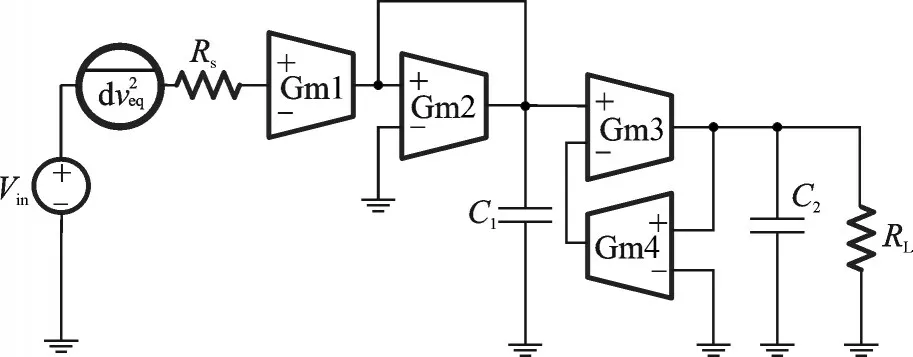
Fig.2 Simplified model of the traditional Gm-C biquad
2 A Current Mode Gm⁃C Biquad
To reduce noise and improve the linearity of a Gm-C filter,several current mode filters were pro⁃posed[14-19].Among them,Ref.[16]introduced a high linearity current mode noise shaping filter.But its bandwidth was only 2.8 MHz,which is not feasi⁃ble for the wideband applications.The filter present⁃ed in Ref.[19]had a bandwidth of 1 GHz but a lim⁃ited IIP3.To solve above issues,a high speed,low noise and high linearity current mode Gm-C biquad is proposed in this paper,as shown in Fig.3.
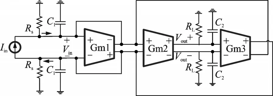
Fig.3 The proposed current mode biquad
The proposed biquad makes use of a high lin⁃earity complementary OTA shown in Fig.4 as its unit Gm cell.In the OTA structure,both NMOS pair and PMOS pair have been utilized for the input transistors,employing the same bias current.The current reuse technique has greatly increased the power efficiency of the circuit.The transistorsMPandMNare added to act as the source degeneration resistors,improving the linearity of the OTA with an ability of transconductance adjustment.Besides,MNis made by two identical transistors with the middle nodeVNusing for the common mode voltage in the common-mode feedback(CMFB)circuit.In this way,extra sensing resistors,are not needed for the common mode voltage.Moreover,since the OTA’s common-mode output voltage is susceptible to the common-mode input signal disturbances and current source mismatches,the CMFB circuit shown in the right part of Fig.4 is utilized to stabi⁃lize it.
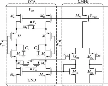
Fig.4 OTA structure including a CMFB
As shown in Fig.3,the proposed current mode biquad consists of three OTAs,four capacitors and twoRL.The structure gets rid of the first voltage to current transformation OTA in the traditional Gm-C filter.In this way,the nonlinearity components com⁃ing from the first OTA in Fig.1 can be reduced.Be⁃sides,the input interferers can be filtered with the help of input capacitorC1before they enter the non⁃linear device.As a result,the proposed filter can achieve a very good IIP3 performance.
The transfer function of the proposed biquad is given by

wheregm1,2,3=gm.
Clearly,a second order low-pass function can still be realized by the structure,except that its in⁃put signal is in current domain.With calculation,the cut-off frequency of the current mode biquad is

and the quality factor is

whereω0is decided by the values ofgmand the ca⁃pacitorsC1andC2.Since large sizes ofM1andM2generate largegmbut also large parasitic capaci⁃tance,an optimized value ofgmis chosen to be 1.7 ms in order to achieve a bandwidth of 5 GHz.Meanwhile,C1andC2are designed as 60 fF and 200 fF,leaving a certain margin for the layout of par⁃asitic capacitance.Since the direct current(DC)gain of the OTA should be larger than 30 dB in a lowQfilter[4],the OTA gain is set to be 35 dB in this parper.Normally,the CMFB circuit needs sense resistorsRto provide the common mode volt⁃age.However,large sense resistors not only occupy large layout area,but also increase parasitic capaci⁃tance and degrade the OTA speed performance.As explained before,because of using the middle node of the active resistanceMN,the large sense resistorRcan be avoided in the design.
3 Comparison of Simulation Re⁃sults Between the Proposed Cur⁃rent Mode Gm⁃C Biquad and the Traditional Gm⁃C Biquad
In order to compare the noise performances of the traditional voltage mode and the proposed cur⁃rent mode filters,source resistors are added at the in⁃puts of the two Gm-C biquads to represent the out⁃put impedance of their previous stage,as shown in Fig.2 and Fig.5.In this way,these two filters have the same representations for their source resistances.As described in Section 2,the input equivalent noise of the voltage mode filter is represented byIn contrast,the current mode filter is actually driven by a current source,its input equivalent noise is repre⁃sented byThen the calculation of the two filters’NF can be simplified as Eqs.(5,6)[20].
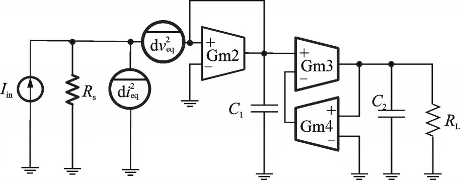
Fig.5 Noise model of current mode biquad including source resistors
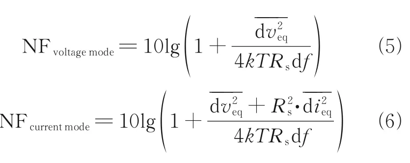
wherekis the Boltzmann’s constant,Tthe absolute temperature,andfthe frequency.Apparently,the NF of the voltage mode Gm-C filter is reverse pro⁃portional to its source resistanceRs.As a result,it will decrease whenRsincreases.Differently,the NF of the current mode Gm-C filter has an optimum val⁃ue whenRsis small.Consequently,the filter with a low source resistance should choose the current mode structure to improve its noise performance.Be⁃sides,from Eqs.(5,6),it can be seen that the NF is not influenced by the gain of two filters,meaning that the load impedanceRLwill not affect their NFs.
For a fair performance comparison,the same OTA with a fixedgmvalue for high-speed applica⁃tions,shown in Fig.4,is used in the traditional volt⁃age mode and the proposed current mode filters with their source impedanceRssetting to 150 Ω.The DC voltage gain of the filters is defined asADC=Vout/Vin,which is also influenced byRL.Both fil⁃ters have been designed with the sameADCby using of suitableRL,which will not affect the noise perfor⁃mance as explained before.Fig.6 shows the simulat⁃ed transfer functions of the proposed current mode and traditional voltage mode filters.Clearly,these two filters have very similar lowpass transfer func⁃tions.As indicated,both filters have an DC gain of around 2.5 dB with a similar bandwidth of 5 GHz.Fig.7 shows the NF performances of the filters.Ob⁃viously,in the frequency range from DC to 5 GHz,the NF of the proposed current mode structure is about 5 dB less than that of the traditional structure.In a wideband communication system,a high-speed filter is always needed after a down mixer in a receiv⁃er or after a high-speed digital to analog converter(DAC)in a transmitter.In both cases,the previous stage of the lowpass filter has a relatively low output impedance ranging from 50 Ω to 300 Ω[21-22].There⁃fore,a current mode filter is preferable compared with the traditional structure in these scenarios.
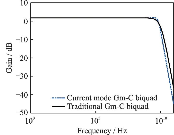
Fig.6 Simulated transfer functions of the traditional Gm-C biquad and the proposed current mode Gm-C biquad
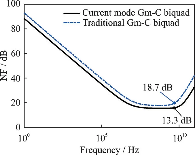
Fig.7 NF of two biquads
Fig.8 shows the simulated IIP3 of the two structures with a 2 GHz and 2.1 GHz two⁃tone test.Clearly,the proposed current mode biquad has an IIP3 value of 35 dBm,which is 6.7 dB better than the traditional voltage mode biquad.
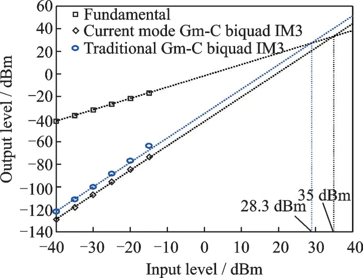
Fig.8 Comparison of IIP3 of current mode and traditional biquad
Besides,the current mode biquad only con⁃sumes 3.2 mW while the traditional one consumes 4.3 mW.The layout of the current mode biquad is shown in Fig.9 with a core area of 0.06 mm2.Table 1 summarizes the simulated results of this paper and compares it with other state-of-the-art results in re⁃cent years.The figure of merit(FoM)used in Ta⁃ble 1 is shown in Eq.(7).Thanks to the proposed current mode Gm-C structure,this paper has the highest speed of 5 GHz,the smallest core area and the best FoM value with very good linearity and noise performances.Accordingly,the proposed cur⁃rent mode Gm-C filter is very suitable for broadband applications with high area-efficiency.
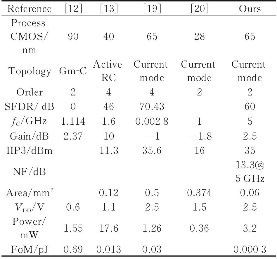
Table 1 Performance comparison with other Gm⁃C fil⁃ters
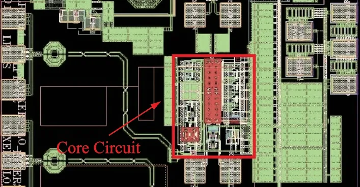
Fig.9 Layout of the filter

whereNpolesis the number of the poles andfCthe cut⁃off frequency.SFDR denotes spurious free dy⁃namic range.
4 Conclusions
A 5 GHz wideband current mode second order filter is presented.By using of a current reused source degeneration OTA,the proposed filter can achieve much better noise and higher linearity per⁃formance with a lower power consumption com⁃pared with the traditional voltage mode filter.This paper is designed in standard 65 nm CMOS technol⁃ogy with a simulated IIP3 of 35 dBm and a power consumption of 3.2 mW.
杂志排行
Transactions of Nanjing University of Aeronautics and Astronautics的其它文章
- Preface
- Generalized Canonical Transformations for Fractional Birkhoffian Systems
- Application of WSGSA Model in Predicting Temperature and Soot in C2H4/Air Turbulent Diffusion Flame
- Hybrid Fault Diagnosis and Isolation for Component and Sensor of APU in a Distributed Control System
- A GPU‑Accelerated Discontinuous Galerkin Method for Solving Two‑Dimensional Laminar Flows
- Thermal Infrared Salient Human Detection Model Combined with Thermal Features in Airport Terminal
