Cleaning of nitrogen-containing carbon contamination by atmospheric pressure plasma jet
2022-09-06LiYANG杨黎SishuWANG王思蜀AndongWU吴安东
Li YANG (杨黎),Sishu WANG (王思蜀),Andong WU (吴安东),
Bo CHEN (陈波)1,Jianjun CHEN (陈建军)1,Hongbin WANG (王宏彬)1,Shuwei CHEN (陈曙嵬)4,Jianjun WEI (韦建军)2,Kun ZHANG (张坤)1,Zongbiao YE (叶宗标)1,∗and Fujun GOU (芶富均)1,∗
1 Key Laboratory of Radiation Physics and Technology,Ministry of Education,Institute of Nuclear Science and Technology,Sichuan University,Chengdu 610064,People’s Republic of China
2 Institute of Atomic and Molecular Physics,Sichuan University,Chengdu 610064,People’s Republic of China
3 Institute of Modern Physics,Chinese Academy of Sciences,Lanzhou 730000,People’s Republic of China
4 College of Physics,Sichuan University,Chengdu 610064,People’s Republic of China
Abstract Atmospheric pressure plasma jet (APPJ) was used to clean nitrogen-containing carbon films(C-N) fabricated by plasma-assisted chemical vapor deposition method employing the plasma surface interaction linear device at Sichuan University (SCU-PSI).The properties of the contaminated films on the surface of pristine and He-plasma pre-irradiated tungsten matrix,such as morphology,crystalline structure,element composition and chemical structure were characterized by scanning electron microscopy,grazing incidence x-ray diffraction and x-ray photoelectron spectroscopy.The experimental results revealed that the removal of C-N film with a thickness of tens of microns can be realized through APPJ cleaning regardless of the morphology of the substrates.Similar removal rates of 16.82 and 13.78 μm min−1 were obtained for C-N films deposited on a smooth pristine W surface and rough fuzz-covered W surface,respectively.This is a remarkable improvement in comparison to the traditional cleaning method.However,slight surface oxidation was found after APPJ cleaning,but the degree of oxidation was acceptable with an oxidation depth increase of only 3.15 nm.Optical emission spectroscopy analysis and mass spectrometry analysis showed that C-N contamination was mainly removed through chemical reaction with reactive oxygen species during APPJ treatment using air as the working gas.These results make APPJ cleaning a potentially effective method for the rapid removal of C-N films from the wall surfaces of fusion devices.
Keywords: N-containing C (C-N) film,plasma-assisted chemical vapor deposition,He-plasma irradiation,atmospheric pressure plasma jet,plasma cleaning
1.Introduction
All-metal plasma-facing materials (PFMs) have been proposed for future fusion to ensure a low erosion rate,low tritium retention and high stability against high neutron flux,which reversely causes the problem of low intrinsic radiation loss in the edge plasma and divertor [1].Consequently,operation in a detached(or partially detached)regime[2,3]is considered necessary to dissipate most of the exhaust heat as radiation and avoid local overheating of the divertor.To reach a detached regime,the general approach is to inject intrinsically low Z or moderate Z impurities,such as N (N,injected as N2) and noble gases (Ne,Ar,Kr,Xe) [4-7],into the scrape-off layer(SOL).The use of chemically reactive N2as a seeding gas is more of a safety challenge for the plant than noble gases [8],but it has the advantage of radiating efficiently at low electron temperatures,which results in the radiation zone from N being mainly located in the divertor region [7].The injection of N2into the SOL produces energetic N ions and thus inevitably leads to a composite with routine C species as co-deposition contamination in the experimental facility [9,10].The co-deposited N-containing C (C-N) layer can serve as a retainer of tritium fuel particles and affects the normal operation of the fusion device.Consequently,requirements for C-N removal are necessary.
To remove this C-N contamination from PFMs,a variety of cleaning methods have been developed,including glow discharging [11,12],laser cleaning [13,14],as well as conventional thermal oxidation [15],mechanical polishing,etc.Despite the promising cleaning result of glow discharging,the cleaning rate remains limited.For example,Peng J et al [16]employed radio frequency glow discharging plasma to clean amorphous C contamination on stainless-steel first mirrors(FMs),which restored the total reflectivity of FM by up to 95%.However,it took about 20 min to realize the removal of a C layer with a thickness of 30-40 nm,corresponding to a relatively low cleaning rate.The mixed contamination layers eroded from the metallic wall structure after detachment treatment would be complicated and different to single amorphous C,and the removal of contamination would be challenging.Cleaning technology based on atmospheric pressure plasma jets(APPJs)[17,18]has been widely used in the process of metal surface cleaning and modification due to hypothermal temperature,dismissal of vacuum installation and generation of sufficient reactive species[19].Due to these advantages,APPJ cleaning shows relatively high cleaning efficiency.Meanwhile,due to the small size and flexibility of the plasma torch,APPJ cleaning is very suitable for the cleaning of components with complex structures.In addition,its application has been extended to fusion-related deposition removal,from thick C co-deposits on the open surface to the C co-deposits distributed along the depth in the castellated gaps [18].
During the actual operation of fusion reactors,plasmafacing components will inevitably be exposed to He plasma,resulting in different substrate conditions for the deposition of C-N layer.Therefore,the cleaning of C-N layer deposited on W substrate with different (pristine flat and He-plasma-irradiated fuzz-covered) surface conditions by APPJ was studied in this work to preliminarily explore the feasibility of APPJ for wall cleaning of a fusion device.Plasma irradiation of the W substrate and preparation of C-N deposits were carried out by employing the SCU-PSI linear device.The cleaning mechanism was investigated through optical emission spectroscopy (OES) and mass spectrometry analysis.
2.Experiments
2.1.Preparation of He-plasma-irradiated W substrates
Polycrystalline W samples(purity 99.9%,10 × 10 × 1 mm3)obtained from Shaanxi Dongji Metal Technology Co.,Ltd,were ground and polished to be used as substrates.To investigate the deposition of C-N film on He-plasma-irradiated W substrate,a pristine W sample was irradiated using He plasma on the SCU-PSI linear plasma device [20],which was based on a single-cathode cascaded arc source and its details can be found in [21].The irradiation was carried out under conditions of DC power of 12 kW with current of 130 A applied to the plasma generator,gas pressure of~2.0 Pa with a He gas flow rate of 5000 standard cubic centimeter per min (sccm),negative bias of 80 V applied to the substrate to increase the energy of incident ions,perpendicular (to the sample) magnetic field of 0.25 T to confine plasma and increase the He ion flux.The He-plasma irradiation lasted for 30 min with stable irradiation temperature of~610°C and He ion flux of 4.2 × 10²²m−2s−1.
2.2.Preparation of C-N film
The preparation of C-N film was performed using DC plasma-assisted chemical vapor deposition with methane(purity 99.999%) and N (purity 99.999%) as reactive gases,and argon (purity 99.999%) to provide plasma and enhance reactivity.The deposition was also carried out on the SCUPSI linear plasma device.The films were grown under deposition conditions of DC power of 8 kW with current of 120 A applied to the plasma generator,total gas pressure of~1.8 Pa with gas flow rates of 2000,150 and 150 sccm for argon,methane and nitrogen,respectively,and negative bias of 30 V applied to the substrates to increase the energy of the incident ions.The deposition process lasted for only 3 min with a substrate temperature of~500 °C.
The setting of the samples in this paper was as follows:(1) He-plasma-irradiated pristine W sample,denoted as W_He;(2)C-N film deposited on pristine W sample,denoted as W_CN and (3) C-N film deposited on He-plasma-irradiated W sample,denoted as W_He_CN.For comparison,the pristine W sample was also involved and denoted as W.
2.3.APPJ processing of samples
After deposition of C-N films,all samples were treated using the APPJ processing device.The schematic diagram of the device is shown in figure 1(a).The device consists of a plasma generator with an actual picture shown in figure 1(b),a power supply system,an air feed system and a three-axis mobile platform.The power supply (Beijing Zhonghai Times Technology Co.,Ltd) operates at a high frequency of 55 kHz with pulse duration of 6 μs and average power of 800 W with working voltage of 2 kV.The plasma generated is a nonequilibrium cold plasma.The APPJ processing was carried out under air flow rate of 50000 sccm,air pressure of 0.5 MPa and a distance of 25 mm between the sample surface and the outlet of the nozzle.The processing time was fixed at 40 s.During the treatment,the temperature was monitored using a thermal infrared imager (FLIR) and pictures were taken every 10 s.
2.4.Materials characterization
The surface morphology of the samples before and after APPJ processing was examined by scanning electron microscopy(SEM,FEI,Inspect F50),and the thickness of deposited C-N films was measured by a 3D optical surface profilometer(SuperView W1,GHOTEST).The phase composition of the samples was determined by grazing incidence x-ray diffraction (GIXRD,Bruker D8 ADVANCE A25) with a fixed incident angle of 0.3°.The elemental composition of the C-N film and chemical bonds between C and N were determined by x-ray photoelectron spectroscopy (XPS,PHI-5000 VersaProbe III,ULVAC-PHI,Inc.).In the x-ray photoelectron spectrometer,a base pressure of 10−7Pa and beam spot size with diameter of 200 μm can be obtained.To analyze the degree of surface oxidation after APPJ treatment,XPS depth profiling was performed using controlled erosion of the surface by ion sputtering.Argon was used as the sputtering gas with a sputtering energy of 2 keV on an area 2 mm × 2 mm.
2.5.Plasma characterization
OES was the only diagnostic technique used in this work to probe the excited levels of atoms or molecules in APPJ due to the invalidation of the Langmuir probe under atmospheric pressure.The broadband spectrum of the arc region of the plasma jet in a wavelength range of 319-870 nm was collected using a 5-channel AvaSpec-UL2048 spectrometer with the optical fiber probe placed 5 mm axial and 50 mm radial away from the outlet of the copper nozzle.The relative position of the optical fiber probe and the plasma jet is shown in figure 1.
3.Results and discussion
3.1.Surface morphology characterization
SEM images of all samples before and after APPJ processing at different magnifications are shown in figure 2.The pristine W shows metallic luster in the optical image,and grain boundaries of polycrystalline W can be clearly seen in the SEM image,as shown in figure 2(a).After He-plasma irradiation,the surface of the W_He is clearly blackened in the optical image,which is caused by the formation of nanofuzzes [22-24],as shown in figure 2(b).After deposition of C-N films,similar curly nanowire structure appears on the surfaces of both W_CN and W_He_CN,as shown in the upper right illustrations of figures 2(c) and (d).However,at the same time,different optical images appear,as shown in the lower left illustrations of figures 2(c)and(d).The surface of W_CN shows better gloss than that of W_He_CN since the deposition occurs on a smooth surface rather than the Heplasma-irradiated rough surface,which is also the reason for the relatively higher porosity of the curly nanowire structure on the surface of W_He_CN.
After APPJ processing,both the optical image and surface morphology of pristine W and He-plasma-irradiated W_He are almost unchanged,as shown in figures 2(a′) and(b′),indicating that no obvious damage was caused to either surface by APPJ processing.APPJ cleaning removes the curly nanowire structure on both surfaces of W_CN and W_He_CN,but leaves behind different substrate structures.The cleaned surface of W_CN is relatively flat and shows metallic luster in the optical image,but sparsely distributed spotty deposits are also observed,as shown in figure 2(c′),which might be a reaction product during the preparation of CN films where a negative bias of 30 V was used since comparison of figures 2(a)and(a′)has shown that APPJ processing does not cause damage to the W substrate.Further study will be carried out to verify this hypothesis in our future work.The cleaned surface of W_He_CN has almost the same morphology as the He-plasma-irradiated W_He surface,with loose fuzz structure,as shown in figure 2(d′),which explains the unobservable change in optical images before and after APPJ processing in figures 2(d) and (d′),and indicates the effective removal of C-N film by APPJ with almost no fuzz damage.
To reveal the above-described cleaning process in figure 2,the thickness change of W_CN and W_He_CN caused by APPJ processing was measured by a 3D optical surface profilometer.For comparison,the thickness of the fuzz layer protruding from the surface of the W substrate was also measured for sample W_He.The measurement area is at the boundary between the W substrate and the fuzz structure or the deposited film,which can be seen from the optical images in figure 2.To improve the accuracy of measurement,splicing measurement was adopted since the single measurement area of the 3D optical surface profilometer is only 482 × 482 μm2.The results are shown in figure 3.Relative to the surface of the original W substrate,the thickness increase caused by deposition of C-N film is 11.21 ± 1.42 μm,as shown in figure 3(a).The thickness of the fuzz layer protruding from the W surface caused by He-plasma irradiation is 6.26 ± 0.58 μm,as shown in figure 3(b).For W_He_CN,the thickness increase caused by fuzz layer growth and C-N film deposition is 16.06 ± 1.88 μm,as shown in figure 3(c).It can be seen that the thickness increase of W_He_CN is not the sum of that for W_He and W_CN,indicating that nanowires of the C-N films are embedded in the fuzz structure and that certain connections may have been formed.
After APPJ processing,the C-N film was fully removed from the surface of W_CN,with no boundary between the substrate and residual film found,as shown in figure 2(c′).This shows that APPJ processing removes the C-N film with a thickness of 11.21 μm in 40 s,corresponding to a removal rate of 16.82 μm min−1.For sample W_He_CN,the C-N layer was also fully removed by APPJ processing,with the fuzz layer left,as shown in figure 2(d).The thickness of the fuzz layer on the APPJ-cleaned W_He_CN surface was also measured,with the result shown in figure 3(d).It can be seen that the fuzz layer thickness on W_He_CN after APPJ processing is 6.87 ± 0.87 μm,which is close to that of the pristine W_He (i.e.6.26 ± 0.58 μm),further demonstrating the effective removal of C-N film from fuzz-covered W surface with complete preservation of the fuzz structure.By comparing figures 3(c)and(d),it can be calculated that APPJ processing removes C-N film with a thickness of 9.19 μm in 40 s,corresponding to a removal rate of 13.78 μm min−1.The difference in removal rate of C-N film for W_CN and W_He_CN is mainly attributed to the difference in surface structure because the interweaving of the fuzz structure and nanowires on W_He_CN will cause errors in thickness measurement of the C-N layer.
3.2.Crystalline structure characterization
To obtain information about changes in crystalline structure on an atomic scale,GIXRD measurements were carried out for all samples before and after APPJ processing,and the results are shown in figure 4.A theta-theta test of pristine W was performed before APPJ processing to determine the peak position and provide reference for the other samples.As shown in figure 4(a),the diffraction peaks corresponding to crystal planes (110),(200),(211) and (220) of W (PDF#04-0806)can be clearly seen for all samples,indicating that W is the main or only crystalline phase within the detection depth of GIXRD,i.e.11.73 ± 0.06 μm for C-based material and 37 nm for W-based material,calculated using the AbsorbDX plug-in of the Diffrac.eva software for the Bruker D8A A25 x-ray diffractometer,and no crystalline phase is formed or with very limited amount since the detection limit of XRD is about 2% [25,26].After APPJ processing,the phase composition does not change and crystalline W is still the only detected phase,as shown in figure 4(b),which indicates that the lattice structure is not affected by APPJ processing since the processing time of 40 s is relatively short and the processing temperature is relatively low,as will be described in the cleaning mechanism study section.
3.3.Element and chemical states characterization
Since the detection depth of the C-based material by GIXRD is at the micron level,even though a grazing angle as small as 0.3° was used,as mentioned above,the use of XPS with a detection depth at the nanometer level is required to understand the chemical structure of the superficial C-N films.This is important for understanding the mechanism of subsequent APPJ cleaning.The XPS survey spectra using a scanning step size of 1 eV are shown in figure 5.The existence of oxygen O 1s signal on all samples before APPJ processing indicates oxidation of the surface and certain adsorption of atmospheric O during the transmission process of the sample,as shown in figure 5(a).It can be seen that the C 1s and O 1s signals of W_He are much stronger than those of W,because the nanoscale fuzz structure on the surface of W_He produces higher surface energy than the flat W surface does,and thus higher C adsorbability and O reactivity.W 4s,W 4p,W 4d and W 4f signals are mainly detected on the surface of pristine W and W_He.The weak N 1s line and strong C 1s line are only observable in the spectra of W_He_CN and W_CN since C-N films are deposited.The content of elements obtained from XPS survey spectra is listed in table 1,from which it can be seen that C accounts for more than 90%of the composition of the C-N film,while N only accounts for about 5%.This indicates that the chemical bonds between N and C might be very limited in the deposited C-N film.
To have better understanding of chemical bonds in the deposited C-N films,high-resolution XPS (HR-XPS) with a scanning step size of 0.1 eV was carried out for W_CN and the results are shown in figure 6,which gives both the original test data and the peak fitting results.The rules of peak fitting using Multipak software can be found in our previously reported paper [27].An area constraint of 4:3 was applied to the spinorbit doublets of the W 4f7/2and W 4f5/2energy levels and their binding energies (BEs) were set apart for 2.18 eV.
As can be seen in figure 6(a),the proportion of C-H bonds is the highest in the C-N film,accounting for 68.35%,followed by C-N bond,accounting for 27.79%.The deconvolution result of the N 1s spectrum reveals the existence of C-N bonds in figure 6(a),and adsorbed N(N-N bond)with BE at 400.45 eV is also detected,as shown in figure 6(b).The trace amount of C-O bonds (3.86%) and N-O bonds (7.77%) recognizedthrough deconvolution of the C 1s line and N 1s line is most likely from environmental contamination since O mainly exists in the form of adsorbed O,as shown in figure 6(c).
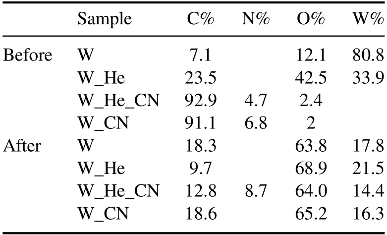
Table 1.Content of surface elements before and after APPJ processing.
After APPJ processing,all samples show a similar XPS survey spectrum,as can be seen in figure 5(b).Obvious peaks of oxygen O 1s,carbon C 1s and tungsten W 4s,W 4p,W 4d,W 4f can be seen in all spectra,and a faintly visible peak of N 1s is only seen in the spectrum of cleaned W_He_CN.It is worth noting that the relative proportion of N (8.7%) on the APPJ-cleaned W_He_CN surface is higher than that (4.7%)before APPJ processing,as shown in table 1.This is most likely due to the formation of W2N during the deposition of C-N film.In the research of our previously reported paper[28],W2N nano-fuzz was prepared through a two-step strategy,with the prior formation of He-plasma pre-irradiated W fuzz followed by N plasma irradiation,similar to the experimental conditions in this work.The significantly reduced intensity of C 1s line for W_CN and W_He_CN demonstrates the effective removal of C-N.It can also be seen from table 1 that the content of C is reduced by about 80% after APPJ cleaning.However,the strikingly increased intensity of the O 1s line also indicates that the surface might have been oxidized during APPJ processing since O makes up 21% of air,the working gas.
To verify surface oxidation and determine whether APPJ processing has caused other composition changes,HR-XPS spectra of the cleaned W_CN sample were measured and the results are shown in figure 7.As can be seen from the deconvolution result of W 4f spectrum in figure 7(a),the doublets with BE at 32.32 and 34.50 eV are associated with W 4f7/2and W 4f5/2of pure metallic W.The other doublets with BE at 36.08 and 38.26 eV are assigned to WO3,which is revealed by the peak of O 1s with BE at 531.03 eV,as shown in figure 7(b).According to the area of peak fitting,the proportion of WO3on the cleaned surface is as high as 70.7%.However,this oxidation should be within a limited depth of nanometers since no oxidation phase was detected by GIXRD,which has a detection depth of 37-46 nm for W and WO3,respectively,calculated using the AbsorbDX plug-in of the Diffrac.eva software for the Bruker D8A A25 x-ray diffractometer.C was still detected on the cleaned surface and mainly existed in the form of C-H bonds,as shown in figure 7(c),which might be caused by environmental contamination.The existence of C-N bonds from the deconvolution results of C 1s also reveals the influence of environmental N contamination to some extent.The C-O bond identified from the deconvolution results of C 1s might be the result of environmental O adsorption,as shown in figure 7(b).
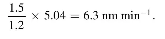
To evaluate the oxidation caused by APPJ processing more objectively,XPS depth profiling was performed to further quantify the depth of oxidation,and the results are shown in figure 8.The sputtering process accumulated for 6 min,and the HR-XPS spectra of W 4f and O 1s were collected with a minimum interval of 6 s to a maximum interval of 1 min.To more accurately characterize the oxidation depth,the etching rate of the instrument at the parameters used was first calibrated with a standard SiO2sample with a thickness of 100 nm.The measured sputtering rate of SiO2is about 4.76 nm min−1and the derived sputtering rate of Si is 5.04 nm min−1.Details of the measurement process can be found in the supplemental file of [27].
In addition,from the measured sputtering rates supplied by the manufacturer,the relative sputtering factors are 1.5 and 1.2 for W and Si,respectively.Thus,the sputtering rate for W is calculated to be:
In figure 8(a),the signal peaks of WO3(BE 35.6 and 37.7 eV)and metallic W(BE 31.3 and 33.4 eV)can be seen on the original surface of pristine W.The intensity of the W 4f components related to WO3disappears clearly after about three times of sputtering,corresponding to a sputtering time of 18 s.Meanwhile,the significantly reduced intensity of O 1s during the first three times of sputtering also reveals the removal of the oxide layer by Ar+sputtering,as shown in figure 8(b).In figure 8(c),the spectra of the APPJ-cleaned surface of W_CN are more complicated than those of W,and a deeper oxidation depth and intermediate oxide of W (such as WO2) may exist.It takes approximately ten times of sputtering for the peak position of W 4f components related to W to stop shifting,as shown in figure 8(c),corresponding to a sputtering time of 1 min.The intensity change of O 1s in figure 8(d) demonstrates that the O 1s signal can be detected even after 15 times of sputtering,corresponding to a sputtering time of more than 2 min.
Figure 9 shows the change in element content with time for pristine W and APPJ-cleaned W_CN during sputtering,from which the variation trend is clearly shown.Figures 9(a)and (b) demonstrate a general trend of decreased O content and increased W content,which indicates a change from WO3to pure metallic W.The O content in the original W sample stabilizes after 0.5 min of sputtering,as shown in figure 9(a),corresponding to an oxidation depth of~3.15 nm(taking into consideration the sputtering rate of 6.3 nm min−1for W).For APPJ-cleaned W_CN,the O content gradually stabilizes after about 1 min of sputtering,as shown in figure 9(b),corresponding to an oxidation depth of~6.3 nm.The analysis reveals that the APPJ-processing-induced oxidation depth(~3.15 nm)is indeed merely at the nanoscale,consistent with the GIXRD result.In addition,figures 8(d)and 9(b)show that the O content of APPJ-cleaned W_CN still decreases at a slow rate after 1 min of sputtering,which might be related to the penetration of O during the preparation of C-N film since O can be adsorbed on W surface and the deposition was carried out at a relatively high temperature of about 500 °C.Further study will be carried out on O penetration in our future work.
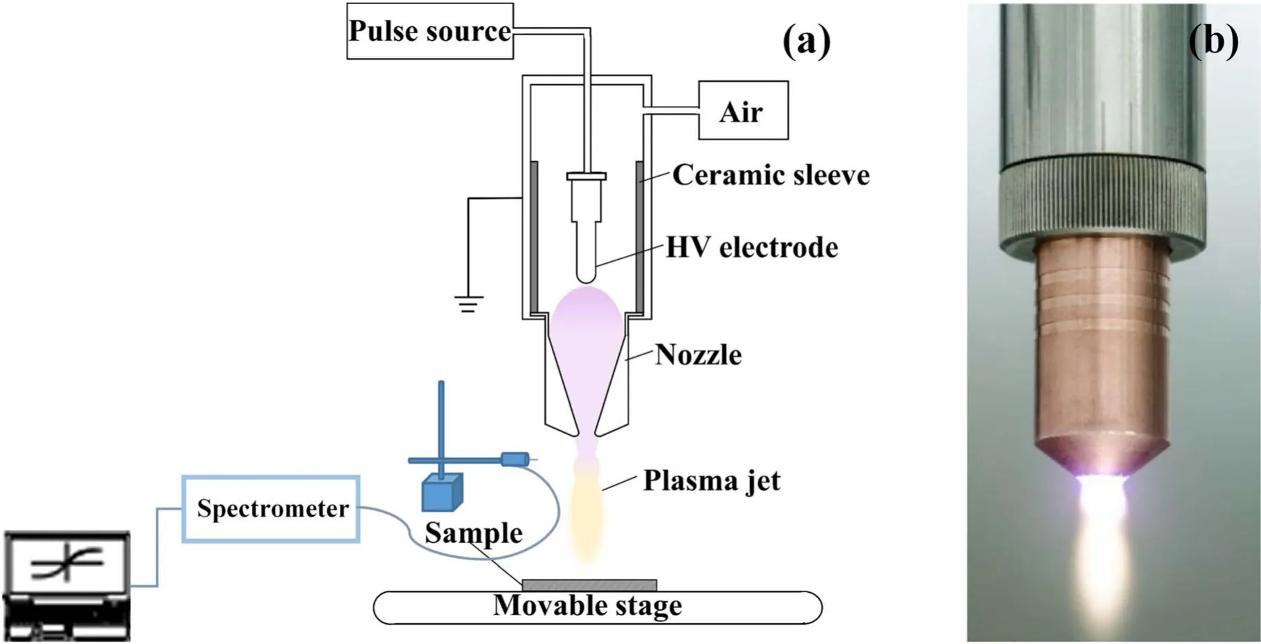
Figure 1.Schematic diagram of the APPJ processing device (a) and an actual picture of the plasma generator in operation (b).

Figure 2.SEM images of W((a),(a′)),W_He((b),(b′)),W_CN((c),(c′))and W_He_CN((d),(d′))before((a)-(d))and after((a′)-(d′))APPJ processing,with corresponding surface optical images shown in the lower left illustrations.
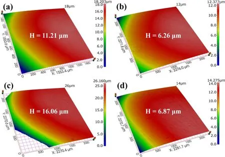
Figure 3.3D optical surface profiles of W_CN (a),W_He (b) and W_He_CN (c) before APPJ processing and W_He_CN (d) after APPJ processing.
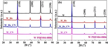
Figure 4.GIXRD patterns of all samples before (a) and after (b) APPJ processing.

Figure 5.XPS survey spectra of the samples before (a) and after (b) APPJ processing.
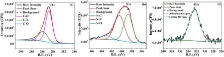
Figure 6.HR-XPS spectra and peak fitting results for W_CN before APPJ cleaning.
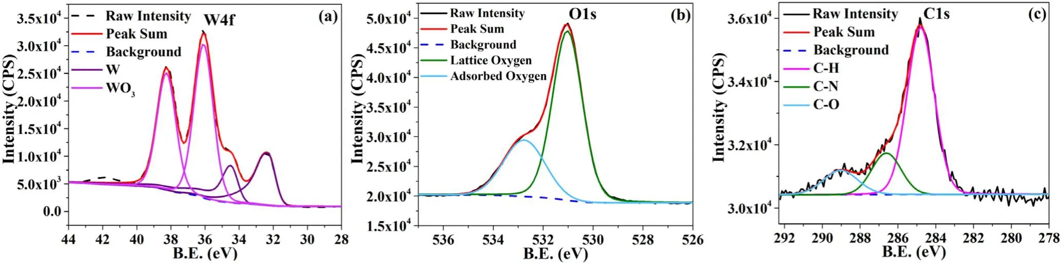
Figure 7.HR-XPS spectra and peak fitting results for W_CN after APPJ cleaning.
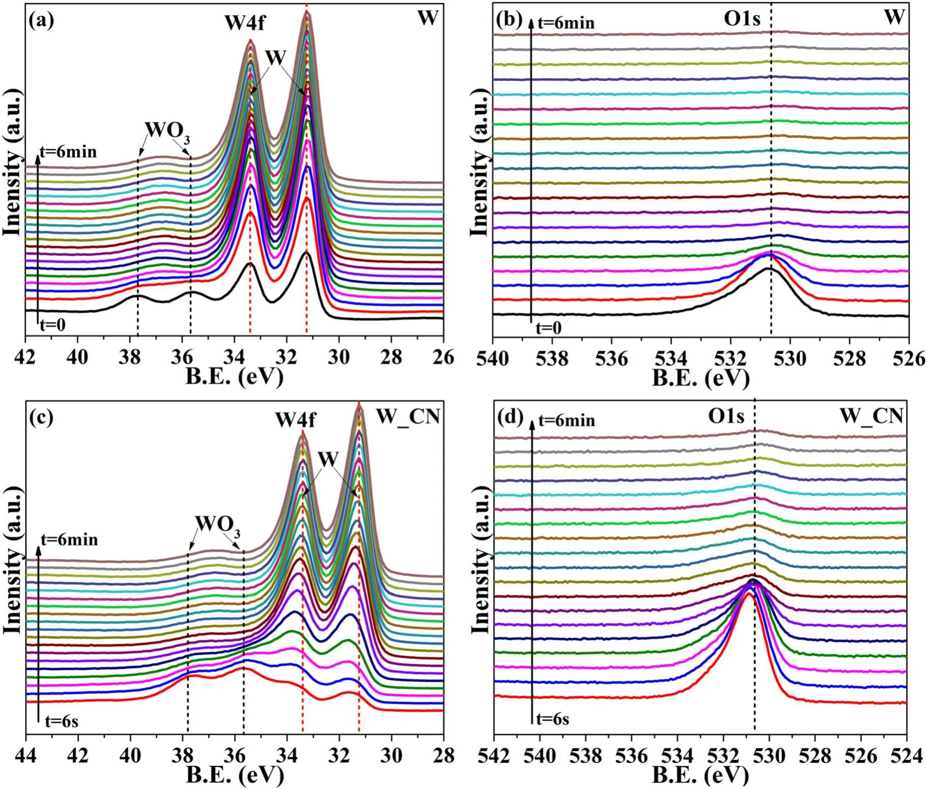
Figure 8.HR-XPS depth profiling for W 4f((a),(c))and O 1s((b),(d))of pristine W((a),(b))and APPJ-cleaned W_CN((b),(d)).Sample surface was sputtered every 6 s in the first minute,then every 15 and 30 s in the second and third minute,and every one minute in the last three minutes.
3.4.Cleaning mechanism study
3.4.1.Real-time surface temperature change and dynamic removal of C-N film during APPJ processing.Postmortem analysis of samples has demonstrated the effective removal of C-N film by APPJ and slight oxidation of the sample surface.However,the mechanism of C-based contaminant removal during cleaning remains to be further understood to comprehend the extended use of this APPJ cleaning method.To study the mechanism of C-N film removal by APPJ cleaning,an FLIR infrared thermal imager and optical camera were respectively used to monitor the real-time temperature change of the sample surface and record the dynamic evolution of the C-N film removal during the APPJ cleaning process.
The time-varying temperature distribution profiles of all samples are shown in figure 10(a),with a temperature recorded interval of 10 s.The indicative color card on the left of the image shows the temperature distribution represented by different colors.Figure 10(a) shows that the surface temperatures of W_He and W_He_CN are higher than those of W and W_CN,which is caused by the formation of poorly thermal-conductive fuzz structure [24],as shown in figure 2(b).It can also be seen in figure 10(a)that the surface temperature of the samples does not show significant change with time except for that of W_CN.The relatively constant temperature on the W and W_He surfaces during APPJ processing can be attributed to the absence of deposition removal from their surface.The expansion of the lowtemperature zone on the surface of W_CN may be related to the removal of C-N deposition and the exposure of W substrate since the temperature distribution on W_CN is similar to that of W after APPJ processing for 30 s.While the insignificant temperature change on the surface of W_He_CN is due to the presence of poorly thermal-conductive fuzz structure after removal of C-N deposition,as shown in figure 2(d′).
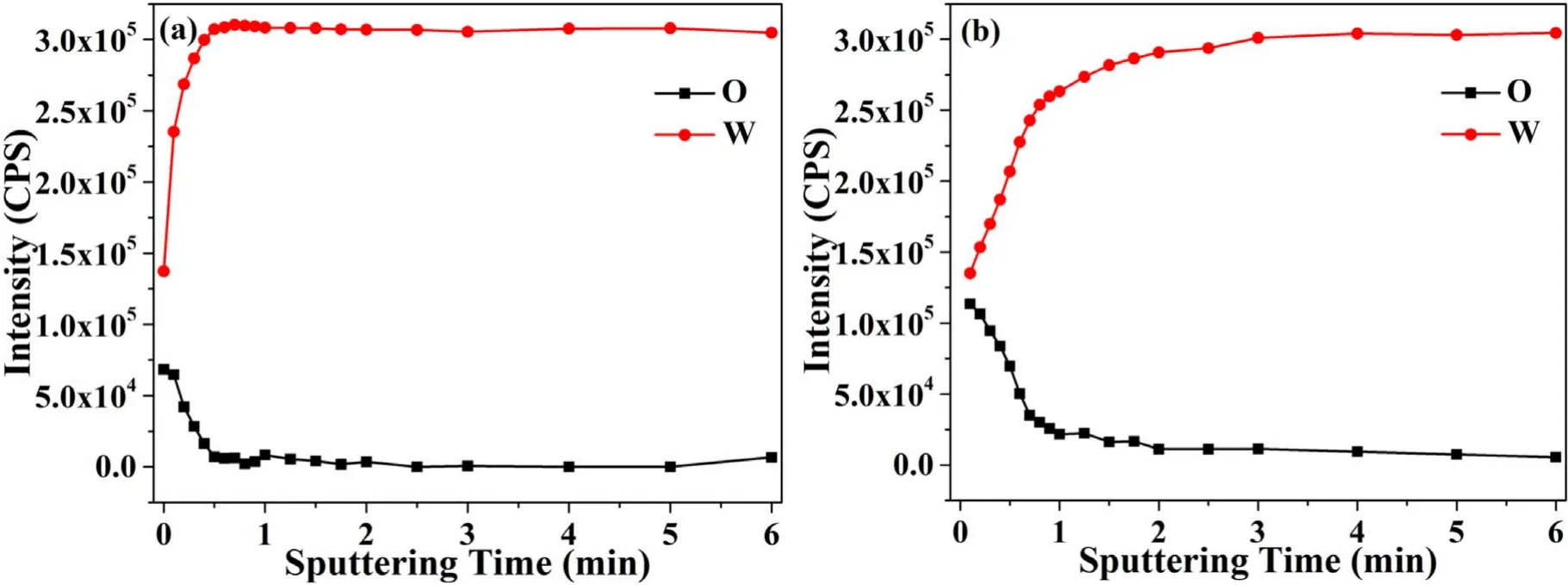
Figure 9.Change in element content with time for pristine W (a) and APPJ-cleaned W_CN (b).
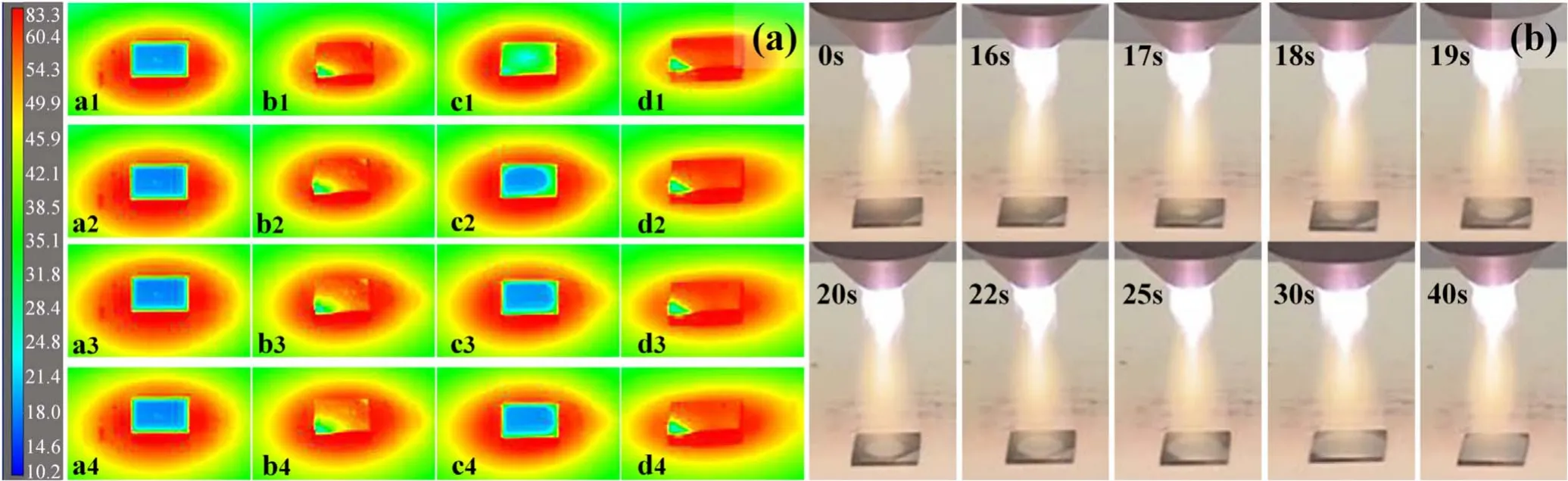
Figure 10.Time-varying temperature distribution profile taken by an infrared thermal imager(a)and optical images of W_CN during APPJ processing(b).Letters a,b,c and d in(a)represent the samples W,W_He,W_CN and W_He_CN,respectively,and the numbers 1,2,3 and 4 represent the times the images were taken,i.e.10,20,30 and 40 s,respectively.
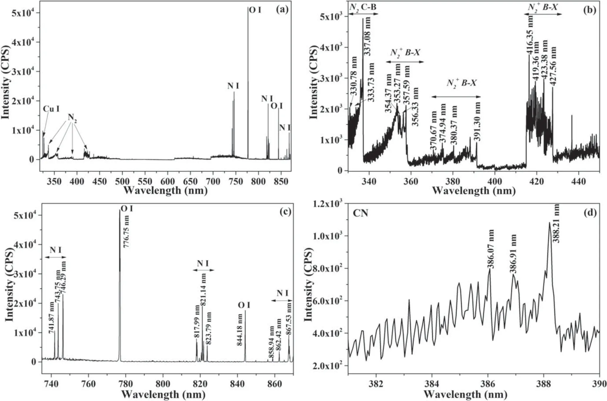
Figure 11.Broadband spectrum of the APPJ(a)and corresponding amplification of excited molecular spectrum(b),atomic spectrum(c)and CN spectrum (d).
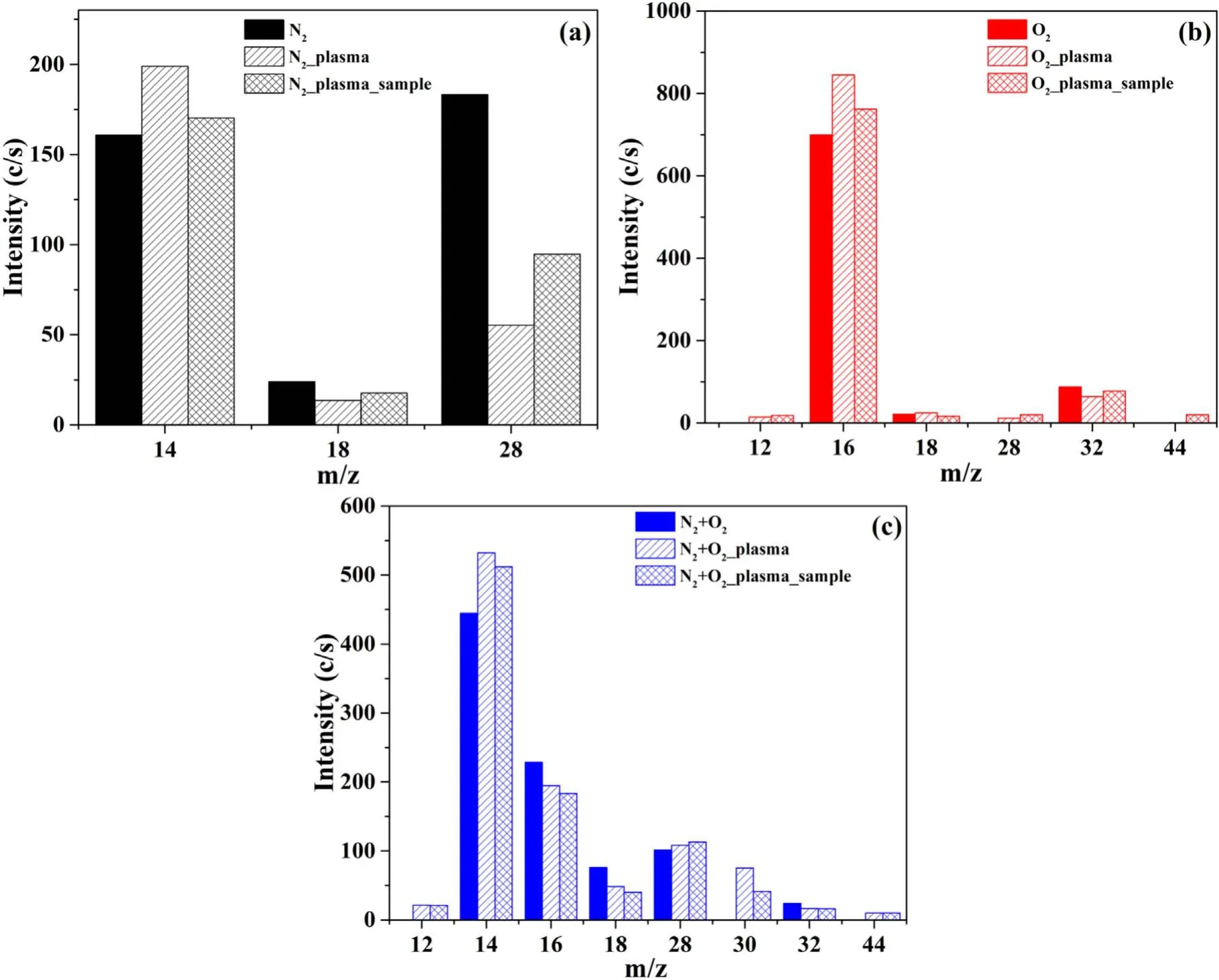
Figure 12.Concentration of ions with different mass-to-charge ratios during cleaning.(a),(b) and (c) are for residual gas analysis under nitrogen plasma cleaning,oxygen plasma cleaning and mixed (N2 and O2 with the air ratio) plasma cleaning,respectively.
The average temperature of the sample surface is listed in table 2,from which the temperature change of the sample surface over time can be clearly seen.The area chosen for calculating the average temperature is a square area with side length of about 5 mm in the center of the sample.It can beseen that the surface temperature of the sample is only tens of degrees Celsius,which is due to the relatively short processing time and relatively long distance between the nozzle and the sample (25 mm,the working distance is 5-30 mm),The slight temperature rise of the pristine W sample during APPJ processing may be due to the thermal effect caused by plasma bombardment [29,30].The relatively high surface temperature of the W_He sample is because the He bubbles under the fuzz structure are poorly thermalconductive [31],which weakens the heat-conducting capability.The surface temperature of the W_He_CN sample is also relatively high and slightly increases during APPJ processing,which is caused by the removal of the C-N film and exposure of the poorly thermal-conductive fuzz-covered surface,as shown in figure 2.The surface temperature of the W_CN sample first decreases and then increases during plasma processing.The decrease in temperature is due to the effective removal of the C-N film and exposure of the high thermal-conductive W surface,while the subsequent increase in temperature is due to the plasma bombardment on the sample surface.
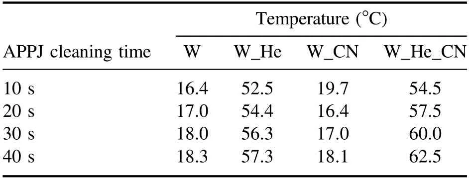
Table 2.Average surface temperature of samples during APPJ processing.
To further establish the visual relationship between surface temperature and C-N film removal,optical images at different times were captured from the recorded video of the cleaning process of W_CN to characterize the dynamic change in surface properties,as shown in figure 10(b).It can be seen from figure 10(b) that the edge of the cleaned area gradually extends outwards from the contact point with the center of the APPJ,which is related to the Gaussian distribution of plasma with high electron density in the center and low electron density in the edge.The cleaned spot did not appear until about 15 s after APPJ cleaning.Therefore,no low-temperature zone caused by substrate exposure appears in the temperature distribution profile taken by the infrared thermal imager,which can be seen from the uniform green color (corresponding to uniform temperature)on the sample surface in the c1 image of figure 10(a).When the cleaning time reaches 30 s,it can be seen that the cleaned area has almost expanded to the whole surface except for the four corners,which is consistent with the blue area(corresponding to relatively low temperature)in the c3 image of figure 10(a).
As discussed in section 3.3,stationary cleaning by APPJ resulted in surface oxidation with a depth of 3.15 nm within 40 s of cleaning time.However,it can be seen that C-N film removal at a single point actually takes only about 15 s from the time-varying optical images during APPJ processing,as shown in figure 10(b).Therefore,if mobile cleaning and strict control of cleaning time are implemented,reduction of the oxidation degree of the substrate can be achieved.In addition,the removal rate of 16.82 μm min−1mentioned above in section 3.1 is also based on the 40 s cleaning time,which is an average cleaning rate.In fact,the cleaning rate of a single point can be as high as 44.84 μm min−1if a 15 s cleaning time is used,and with the three-axis mobile platform,the distance between the sample surface and the outlet of the nozzle can be adjusted,thus further improving the cleaning efficiency.
3.4.2.OES analysis.The study of plasma cleaning mechanism is inseparable from the study of plasma characteristics,but traditional invasive techniques with low spatial resolution are not suitable for APPJs with small dimensions and significant non-uniformity since they yield incorrect mean values and significantly disturb the plasma properties [32].Non-invasive optical diagnostic techniques are thus the methods of choice for the diagnosis of APPJ [33].To explore the interaction mechanism between APPJ and C-N film,effective nonperturbing OES analysis was implemented to identify the presence of excited species within the plasma.An indicative broadband spectrum of the arc region of the plasma jet in a wavelength range of 319-870 nm is shown in figure 11(a),with corresponding amplification of excited molecular spectrum and atomic spectrum shown in figures 11(b) and (c).The Cu I emission lines labeled in figure 11(a)were due to nozzle erosion by the plasma jet.N2second positive system and N2first negative system bands [34]covering the 330-450 nm range were identified in figure 11(b).Atomic O and N lines in the 730-875 nm range are identified in figure 11(c).Peaks of CN(B-X,violet system) were identified in the 380-390 nm wavelength range with moderate emissions at 386.07,386.91 and 388.21 nm [34,35],as shown in figure 11(d).Thus,the excited species in the APPJ include molecules of N2and CN,and atoms of O,N and Cu.Among them,excited O and N atoms,and excited N2molecules might be reactive species that can promote C-N film removal,while CN might be the reaction product of excited N species and C-N film or with ambient C.Combined with the analysis of surface composition before and after cleaning,as shown in section 3.3,the active O atoms may have played a major role in the removal of C-N film,since oxidation occurs on the sample surface after cleaning,as shown in figures 8 and 9.
3.4.3.Mass spectrometry analysis.To verify our hypothesis,the intermediate products during APPJ cleaning were detected by mass spectrometry to deepen our understanding of the cleaning mechanism.Considering the difficulty of collecting reaction products in an open space during APPJ cleaning,we explored the cleaning mechanism in a vacuum chamber using an inductively coupled plasma source and a mixture of N2and O2with an air ratio.A schematic diagram of the experimental apparatus can be found in our early reported paper [36].For comparison,the intermediate products obtained using nitrogen or oxygen plasma cleaning alone were also studied.The intensity to mass-to-charge ratio (m/z) distributions of ions analyzed by mass spectrometry is shown in figure 12.
As shown in figure 12,the ions with m/z ratios of 12,14,16,18,28,30,32 and 44 could be assigned to C+,N+,O+,OH2+,N2+/CO+,NO+,O2+and CO2+[37],respectively.During nitrogen plasma cleaning of W_CN,no C-related products were detected,as shown in figure 12(a),indicating that the reactions between C-N film and N plasma are limited.The ions with m/z ratios of 28 and 44 clearly indicate the existence of CO and CO2during oxygen plasma cleaning of W_CN,as shown in figure 12(b),which reveals the speculation in section 3.4.2 and is in accordance with the oxidation of the W substrate after APPJ removal of C-N film from W_CN,as discussed in section 3.3.The ions with the m/z ratio of 30 during cleaning with mixed nitrogen and oxygen plasma might be NO originating from the combination of N+and O+,as shown in figure 12(c).It should be pointed out that the mass spectrometry analysis was carried out in the order of gas,plasma-sample interaction and single plasma (N2→ N2_plasma_sample → N2_plasma for N plasma cleaning,for example) since it was impossible to separate the C-N film from the plasma when measuring the mass spectrum of the plasma.Thus,the12C+,30NO+and44CO2+ions observed in the mass spectrum of single plasma are most likely the residual reaction product of C-N film with plasma.
Therefore,the above experimental results give a view of a typical plasma-chemical cleaning process as below:
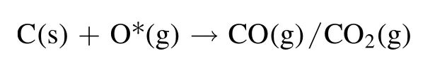
The combined analysis of OES and XPS shows that reactive O species play a major role in removing C-N contamination by APPJ cleaning using air as the working gas.
4.Conclusion
N-containing C (C-N) films were deposited on pristine flat and He-plasma pre-irradiated fuzz-covered W substrates through pyrolysis of methane using a high-density linear plasma device.The obtained films had loose nanowire structure with a thickness of 11.21 ± 1.42 μm,and were mainly composed of C and a small amount of N.
APPJ processing technique was used for the removal of C-N films,and the results showed that APPJ can quickly and effectively remove the C-N films from pristine flat and Heplasma-irradiated fuzz-covered W surface with a removal rate of up to 16.82 μm min−1,while restoring the integrity of the substrate morphology.GIXRD and HR-XPS spectrum results indicated that surface oxidation occurred at limited nanoscale depths after APPJ cleaning.Through HR-XPS depth profiling,the oxidation depth induced by APPJ processing was estimated to be a mere 3.15 nm.Time-varying optical images during APPJ processing indicated that the removal of C-N occurred from the center to the edge in the form of a circle,and it actually took only about 15 s for the removal of C-N film at a single point,providing a way to reduce substrate oxidation and improve cleaning efficiency through mobile cleaning.Spectral analysis indicated that mainly atomic O and atomic N reactive species existed in APPJ.Mass spectrometry analysis revealed that the removal of C-N film was mainly realized through chemical reaction with atomic O.
This study provides a reference for the use of APPJ cleaning as a method for the quick removal of C-N film,which can be used as a supplement to other cleaning methods for the removal of fusion-related deposits,especially those that are thick or in castellated structures.In future work,the focus will be on the reduction of substrate oxidation through mobile cleaning and the removal of C-N film from castellated structures.
Acknowledgments
This work has been funded by National Key Research,Development Program of China (No.2017YFE0301305-KYWX-002) and Sichuan Science and Technology Program(No.2021YFSY0015).
猜你喜欢
杂志排行
Plasma Science and Technology的其它文章
- Study of a 105 GHz short-pulse dummy load for the electron cyclotron resonance heating system with the quasi-optical method
- Impacts of laser pulse width and target thickness on laser micro-propulsion performance
- The effects of dilution gas on nanoparticle growth in atmospheric-pressure acetylene microdischarges
- The effect of nitrogen concentration on the properties of N-DLC prepared by helicon wave plasma chemical vapor deposition
- Development of low power non-thermal plasma jet and optimization of operational parameters for treating dyes and emerging contaminants
- A comparison of power measurement techniques and electrical characterization of an atmospheric pressure plasma jet