Photoexcited carrier dynamics in a GaAs photoconductive switch under nJ excitation
2022-08-01MingXU徐鸣YiWANG王毅ChunLIU刘春XinyangSI司鑫阳RongrongGAO高荣荣WeiLUO罗伟GuanghuiQU屈光辉WanliJIA贾婉丽andQianLIU刘骞
Ming XU(徐鸣),Yi WANG(王毅),Chun LIU(刘春),Xinyang SI(司鑫阳),Rongrong GAO(高荣荣),Wei LUO(罗伟),Guanghui QU(屈光辉),Wanli JIA(贾婉丽)and Qian LIU(刘骞)
Applied Physics Department,Xi’an University of Technology,Xi’an 710048,People’s Republic of China
Abstract In this article,the bunched transport of photoexcited carriers in a GaAs photoconductive semiconductor switch(PCSS)with interdigitated electrodes is investigated under femtosecond laser excitation.Continuous outputs featuring high gain are obtained for single shots and at 1 kHz by varying the optical excitation energy.An ensemble three-valley Monte Carlo simulation is utilized to investigate the transient characteristics and the dynamic process of photoexcited carriers.It demonstrates that the presence of a plasma channel can be attributed to the bunching of high-density electron–hole pairs,which are transported in the form of a highdensity filamentary current.The results provide a picture of the evolution of photoexcited carriers during transient switching.A photoinduced heat effect is analyzed,which reveals the related failure mechanism of GaAs PCSS at various repetition rates.
Keywords:GaAs PCSS,high gain(HG),plasma channel,filamentary current,heat effect
1.Introduction
Gallium arsenide photoconductive semiconductor switches(GaAs PCSSs)have extensive applications,such as pulsed power systems,terahertz emitters,plasma technology,and high-speed electronics[1–4]due to their ultrafast response time,low jitter,optical trigger isolation,and ease of integration[5–10].The most attractive feature of GaAs PCSSs is the process of photoexcited carrier multiplication by impact ionization after the removal of external optical excitation,which results in a reduction of the required optical excitation energy.This avalanche operation is known as the high gain(HG)or nonlinear mode,even if optical energy on the scale of microjoules(μJ)or nanojoules(nJ)is employed[11–14].Although HG GaAs PCSSs have the technical potential to be used in compact and palm-size systems at low optical energy,a stronger bias electric field would simultaneously be required across an electrode gap[15,16].Consequently,this would reveal the presence of nonuniformities in the strong electric field and induce the spatial structures of current flows with different current density values in the semiconductor.Specifically,the bunched transport of photoexcited carriers is accompanied by the formation of filamentary currents,which leads to highly conductive plasma channels.In other words,these high-density filamentary currents nucleate above a certain applied electric field strength,which inevitably results in the overall failure of the GaAs PCSS.
Based on the above issues,it is exigent to optimize the transient distribution of the electric field,especially at high repetition rates.In this regard,many studies have been devoted to alleviating these autocatalytic highly conductive carrier channels in semiconductors and improving device longevity[17–19].These studies have typically focused on fabricating modified deeply diffused,epitaxially grown contacts.Simulations have been performed which identified that the spatial nonuniformities can be quenched by strong uniform illumination[20].Alternatively,multiple filaments can be produced to share the current,which is performed by multiline triggering at high current levels for better device longevity[6,21].Time-resolved laser thermal reflectance has been employed to investigate the picosecond-scale Joule heating of the photoconductive switch electrodes[22].
To develop a phenomenological theoretical description of the HG operation,in particular,the nucleation and growth of filamentary currents in GaAs PCSSs,an interdigitated GaAs PCSS with micrometer gaps is designed with a femtosecond(fs)optical excitation of hundreds of nJ.Outputs are obtained under different optical excitations,and the corresponding transient currents and current densities are numerically quantified relative to the bias electric electric field.The dynamic process of this photoexcited plasma channel is demonstrated in HG operation.The corresponding thermal effect is quantitatively analyzed at a 1 kHz repetition rate.
2.Experimental setup
The schematic of a GaAs PCSS is shown in figure 1,which is a lateral structure in the experiment.A semi-insulating(SI)GaAs wafer is utilized as the substrate material,whose dark resistivity and the electron mobility are 5×10⁷Ωcm and more than 6000 cm2/(Vs),respectively.Interdigitated electrodes are deposited on the surface of the SI GaAs substrate,whose contact metallization consists of 200 nm of gold(Au)and 5 nm of chromium(Cr).The width and gap of the interdigitated electrodes are both 5 μm,which is suitable for full coverage of the optical spot.A sputtered 560 nm Si3N4layer is fabricated on the GaAs surface for passivation and insulation purposes.In the experiments,a titanium(Ti)sapphire laser is used as the optical trigger source,whose full width at half maximum is 100 fs at a wavelength of 800 nm(~1 μm optical absorption depth in GaAs).A beam splitter is utilized to split the incident optical pulses into two identical parts.One is used to excite the interdigitated electrodes,while the other is used to measure the optical energy with an optical energy meter(J-10Si-HE,200 pJ–400 nJ and J-10MB-LE,300 pJ–600 μJ).
The test circuit used with the GaAs PCSS is shown in figure 2.The ceramic capacitor,which is charged by a DC voltage source through a 10 MΩ resistor,provides a sufficient voltage or electric field to bias the PCSS so that the threshold condition of an electric field can be satisfied in HG mode.Moreover,an oscilloscope(LeCroy HDO4104,6 GHz,4×40 GS s-1)is utilized to record the output waveforms,which are attenuated by a 20 dB attenuator.In addition,a coaxial line is used between the GaAs PCSS and the attenuator.To shed light on the spatiotemporal characteristics of the plasma channel in HG operation,the relevant experiments and simulations are performed under different bias electric fields with fixed optical excitation energies in HG mode.
3.Results and discussion
3.1.HG mode for single shots and in repetitive operation
Due to the negative differential mobility(NDM)effect of GaAs[23],photoexcited carriers in a HG GaAs PCSS have a complicated transport mechanism.The potential process involves many mechanisms,such as impact ionization,photo circulation,and so on.In HG operation,classic persistent conduction can be observed in a GaAs PCSS and the formation of filamentary current takes place.The current density is determined by the filamentary current that is also detrimental to the PCSS’s reliability and stability.The optics and contact structure are designed to produce multiple filaments and share the overall current stress in the device[24].
Figure 3 shows stable switching waveforms for single shots as the optical pulse energy increases from 140 to 500 nJ while the bias voltage is kept at 5 V(i.e.,10 kV cm-1).The results show that the HG modes achieved by single shots are related to the varying optical pulse energy.An unexpected phenomenon is that the amplitude decreases as the optical pulse energy is increased to 500 nJ.This may be caused by the occurrence of ablation on the interdigitated contacts.When the GaAs PCSS is excited under a 10 kV cm-1bias electric field and 140 nJ of optical excitation energy,a large number of high-density electron–hole pairs are generated in the HG GaAs PCSS by avalanche multiplication of carriers.A plasma channel is generated due to the bunched transport of high-density photoexcited electron–hole pairs,in which the heat produced results from the heating effect of the highdensity filamentary current.Considering the occurrence of the HG characteristic under different optical excitations,operation at lower optical excitation levels is beneficial for device stability.Therefore,the optical excitation is decreased to 140 nJ and repetitive operation is then carried out.
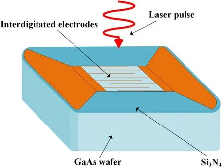
Figure 1.The schematic of the GaAs PCSS used in the experiments.
Figure 4 shows the superposed HG switching waveforms achieved at a 1 kHz repetitive rate.The corresponding optical excitation energy is 140 nJ and the bias electric field is 10 kV cm-1.The superposed switching waveforms illustrate that all of the output transients overlap well and present good stability at a 1 kHz repetition rate,at which the average peak and rise time are 1.356 V and 331 ps,respectively.It is found that the heat accumulation is enhanced by repetitive operation.The results show that the voltage amplitude is higher than that of single-shot operation.This is attributed to heat accumulation during repetitive operation,which leads to carrier multiplication.
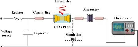
Figure 2.The test circuit used with the GaAs PCSS in the experiment.
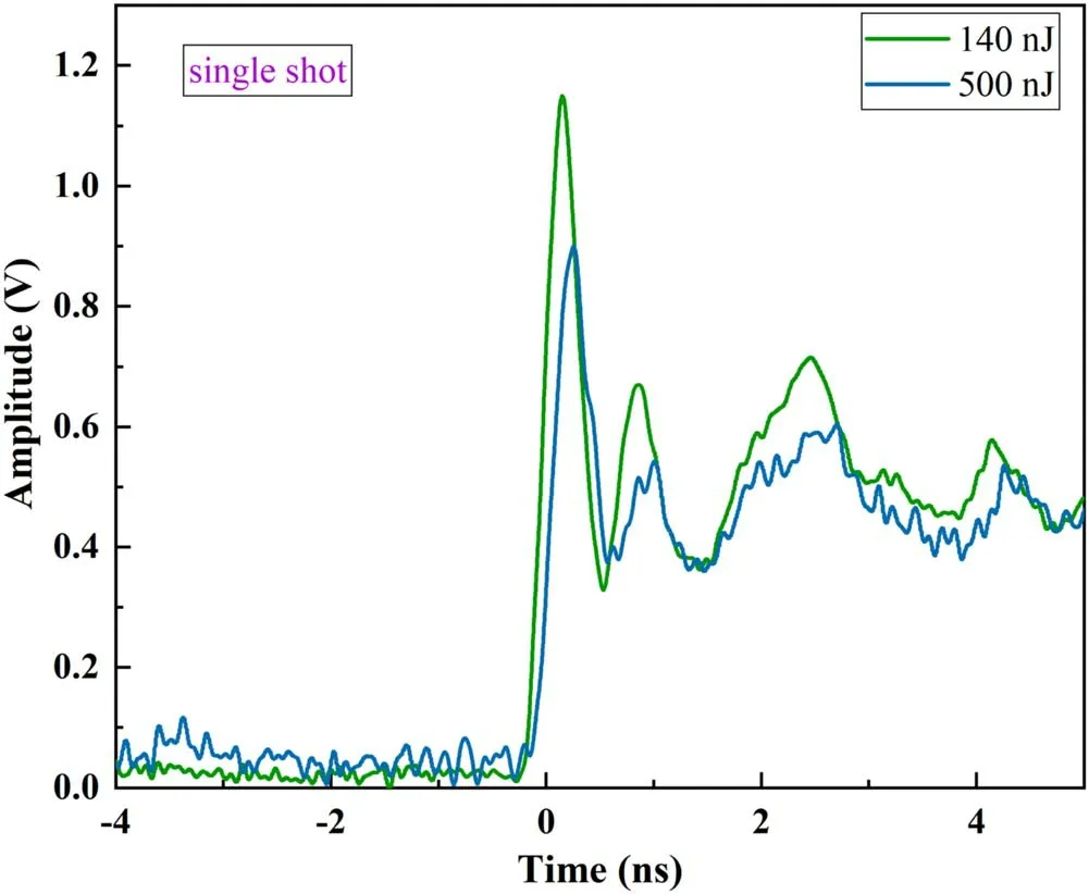
Figure 3.Switched voltage waveforms at optical excitation energies varying from 140(green curve)to 500 nJ(blue curve)under an bias electric field of 10 kV cm-1.
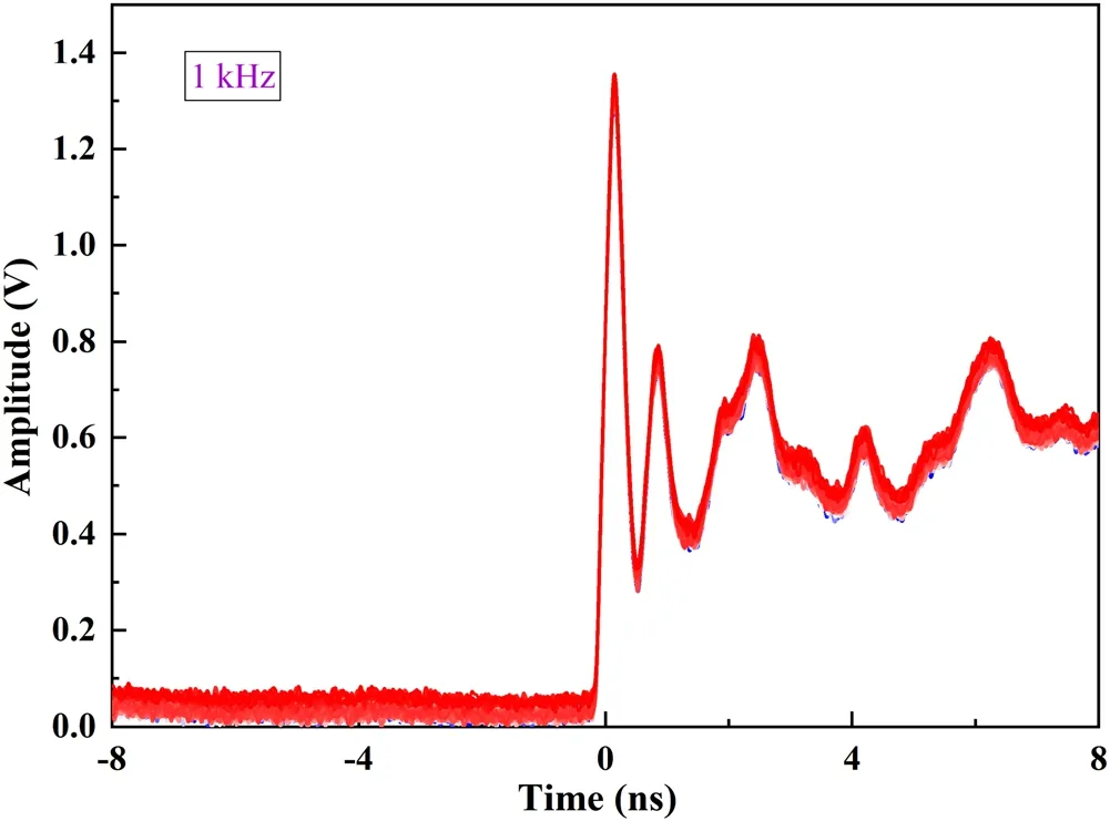
Figure 4.Overlapping voltage waveforms at a 1 kHz repetition rate with an bias electric field of 10 kV cm-1.

Figure 5.Simulations of transient current density(a)and current(b)for bias electric electric fields of 10,15,and 20 kV cm-1,respectively.
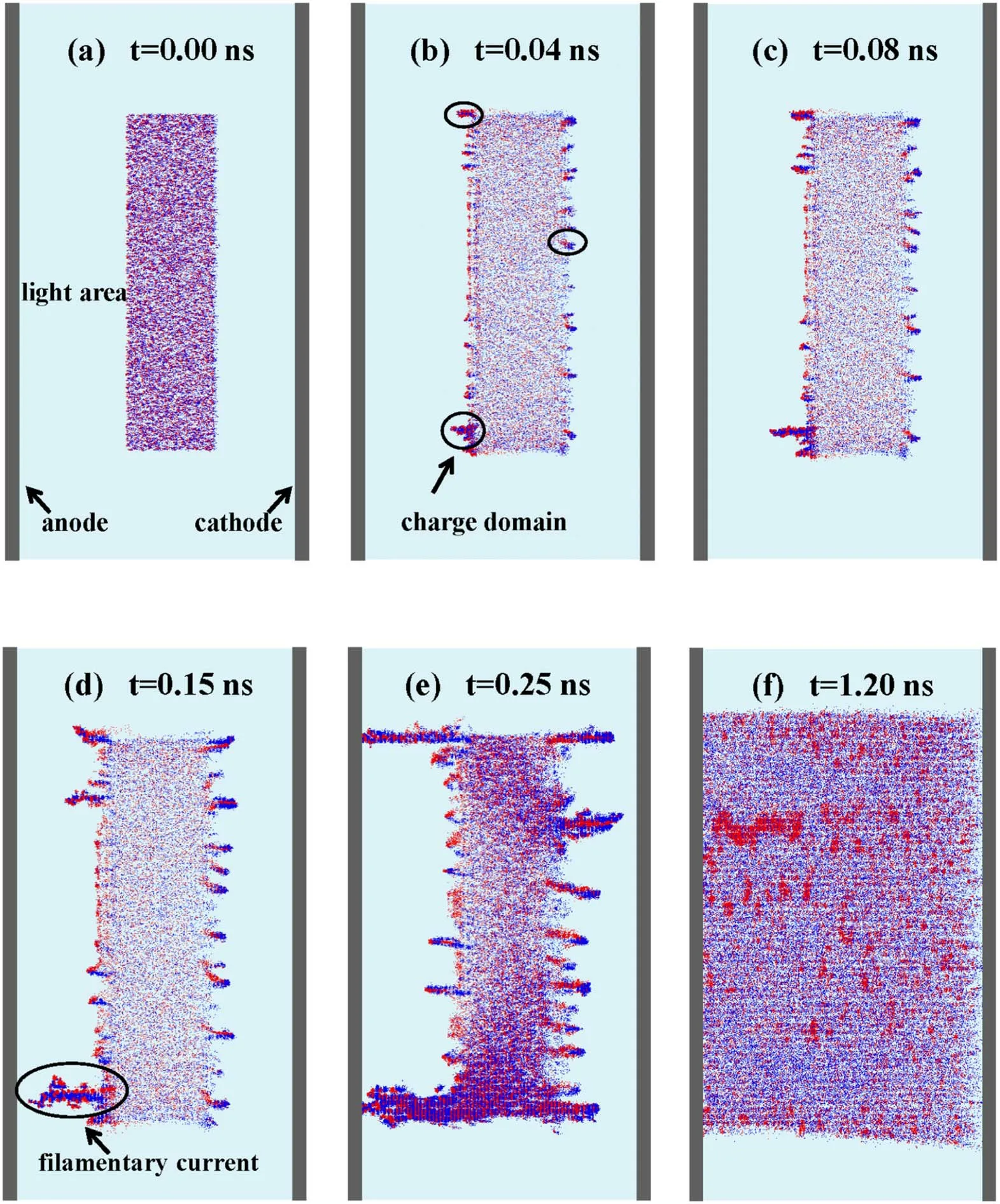
Figure 6.Simulations of transient carrier distributions at an bias electric field of 10 kV cm-1.
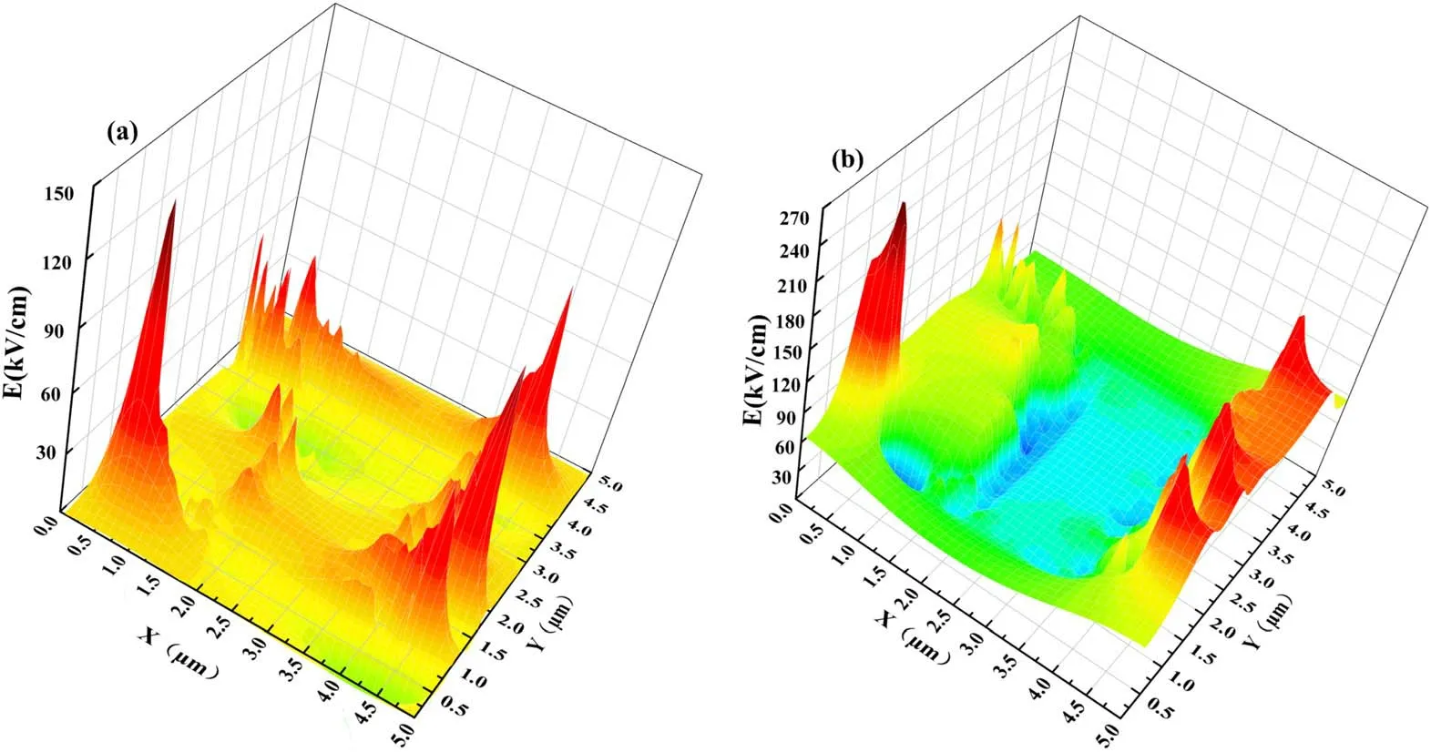
Figure 7.Simulated distribution of the electric field in a GaAs PCSS at different bias electric fields at t=0.15 ns:(a)10 kV cm-1,(b)20 kV cm-1. X is the direction from the anode to the cathode and Y is the direction parallel to the electrodes.
3.2.Photoexcited carrier dynamics
The generation and transport of photoexcited carriers play a significant role in the performance of GaAs PCSSs.Microscopically,the occurrence of filamentary current is an inevitable result of photoexcited carriers’bunched transport in a strong electric field.However,it is difficult to visually demonstrate the relevant temporal transport using macroscopic time-domain switching waveforms.Although timeresolved reflectivity measurements have been performed to detect the carrier dynamics[25],it is not sufficient to describe the photoexcited carrier transport process under a stronger electric field with the HG mechanism.Therefore,Monte Carlo simulation,which can depict the internal physical process,is utilized to investigate the dynamic process of photoexcited carriers under fs laser pulses.
In the Monte Carlo simulation,a band structure of three valleys(Γ,L,X)in the non-parabolic approximation is employed.Moreover,the number of photoexcited carriers cannot be completely determined,but the real concentration of carriers is required when we deal with the Poisson equation and photoconductive current.Hence,in our simulation,the real photoexcited charges are treated as 2×10⁴independent superparticles whose charge is determined by the excitation level,and the time step is set to 10-14s.According to the design of our experiments,only half of the optical excitation energy falls on the active gaps of the device;the rest is reflected by the metal electrodes.Moreover,the optical spot on the interdigitated electrode cell gap approximates a rectangle whose length and width are 3 mm and 5 μm,respectively.The absorptive depth of GaAs for 800 nm fs laser energy is on the order of~μm,which is smaller than the thickness of the GaAs wafer.Therefore,the corresponding initial concentration of the injected photoexcited carriers is calculated to be approximately~1016cm-3.
In our experiment,each electrode gap is paralleled and initiated simultaneously upon the fs optical illumination.The transient from each unit is finally synthesized at the terminal.Hence,the dynamic process of the photoexcited carriers in each gap plays a significant role in the transient characteristics of the switch.The variations of current density with respect to the bias electric field are numerically modeled and shown in figure 5(a).The current density at 10 kV cm-1is 1.3×10⁶A cm-2at 3.6 ps,which gradually stabilizes after 0.04 ns.This indicates that photoexcited carrier bunched transport occurs and consequently forms a charge domain.Note that the creation and transport of the charge domain means that the current density tends to be in a dynamic equilibrium.Meanwhile,the current density rises faster and reaches up to 2.3×10⁶A cm-2when the bias electric field is 20 kV cm-1.This is consistent with the density of the filamentary current reported in the literature[26].This special plasma channel with high current density will inevitably result in the formation of filamentary current.
Theoretically,the current density is determined by the bias electric field,as the charge domain does not arrive at either electrode.The current density can be calculated as follows:

whereJis the current density,qis the quantity of charge per carrier,nis the carrier concentration,μnis the carrier mobility,Eis the bias electric electric field,K0is the Boltzmann constant,Tis the temperature of the GaAs PCSS,and dn/dxis the concentration gradient of carriers parallel to the direction of the electric field.
In equation(1),the current density consists of two parts,including the drift and diffusion of the carriers.The first righthand term is the contribution of the drift motion,and the second right-hand term is the contribution of the diffusion motion.Generally speaking,carrier diffusion can be ignored under a strong electric field,because under such conditions,carrier drift dominates.Therefore,the current density can be modified to read:
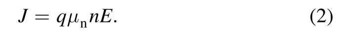
It can be seen from equation(2)that the current density is proportional to the bias electric field.This reveals the relationship between the current density and the bias electric field.In our simulation,as the bias electric field varies from 10 to 20 kV cm-1,the corresponding current density peak increases from 1.3×10⁶to 2.3×10⁶A cm-2,as shown by
figure 5(a).The current density and bias electric field present a more proportional relationship,which conforms with the transport theory of the carriers given in equation(2).
Similarly to the current density in figure 5(a),the transient currents also present the classic lock-on phenomena,which also verifies the HG mode of the GaAs PCSS,as shown in figure 5(b).Normally,the filamentary current with high-density carriers degrades the switch due to Joule heating during the lock-on period[27].The corresponding diameter of the filamentary current in the experiments can be calculated quantitatively by[28]

wheredlockis the diameter of the filamentary current,Seis the cross-sectional area of the filamentary current,Ilockis the current intensity,andJlockis the current density,all of which are during the lock-on period.In our simulation,the value of the lock-on current density in figure 5(a)is 106A cm-2,and the corresponding lock-on current intensity in figure 5(b)is 1 A.Therefore,the calculated diameter of the filamentary current is approximately 11.3 μm,which is consistent with reports in the research literature[29,30].
To gain an insight into the temporal profile of the photoexcited carrier evolution and electric field distribution,the transient characteristics of a gap unit of the interdigitated electrodes are simulated at 10 kV cm-1.The surface of the device is evenly meshed(80×80)to make the calculation process more convenient.Simulations of the transient carrier distribution at 10 kV cm-1are shown in figure 6.In order to decrease the computational requirement,a two-dimensional model is used in the simulation.The red and blue dots are electrons and holes,respectively.A rectangular light area is located in the middle region,and the anode(at the left)and cathode(at the right)are located at the sides,as shown in figure 6(a).It should be noted that the incident laser spot in our simulation is rectangular according to practical geometry.
Att=0 ns,an initial distribution of carriers is produced by the optical excitation,which is concentrated in a rectangular area,as shown in figure 6(a).A number of photons are absorbed in a very short time to form corresponding electron–hole pairs(photoexcited carriers).Subsequently,the photoexcited carriers move separately to electrodes under the force of the electric field,and the built-in electric field increases gradually.Due to the impact ionization in GaAs and the NDM effect under the strong bias electric field of 10 kV cm-1,the carriers near the electrodes are transported in a bunched manner and form charge domains at 0.04 ns,as shown in figure 6(b).It can be seen that carriers pile up at many points and develop into the spatial and temporal structures of current flow,as depicted in figures 6(c)and(d).The carrier concentration in front of the charge domains can be expected to increase further,making the impact ionization more dramatic.In turn,this gives rise to an increase in the number of carriers,while the carriers’radiativerecombination also plays a part.Certainly,the recombination also plays an important role in the following process.The photons generated by the radiative recombination are,in turn,absorbed in turn by the GaAs substrate,which indirectly produces new electron–hole pairs in front of the charge domain.Because the photon velocity is far greater than the electron velocity in GaAs,the successive charge domains begin to branch and form a resulting channel for the filamentary current in space.
As shown in figure 6(e),two filaments apparently reach the anode att=0.25 ns,when the other filaments nucleate and grow further.During this process,the mechanisms of electron–phonon coupling and inelastic impurity scattering contribute to the carrier avalanche multiplication and maintain the filaments’nucleation[31].The power provided to the system goes into the ohmic contacts as the filament reaches the electrodes.Meanwhile,it reduces the electric field supplied to the impact ionization.Eventually,more filaments form as the current increases and the current flow fills the entire GaAs switch.The number of photoexcited carriers remains in a dynamic balance when the current density is distributed uniformly,as shown in figure 6(f).
Although the transient transport of photoexcited carriers is microscopically represented by the phenomenological description,the electric field plays a key role in the output characteristics of GaAs PCSSs.Therefore,simulations of the transient
field distribution att=0.15 ns are performed,as shown in figure 7.At this moment,the filamentary currents have apparently formed but have not yet arrived at the electrodes,as shown in figure 6(d).To compare the spatial distribution of the electric field,simulations are carried out for two different bias electric fields,10 kV cm-1and 20 kV cm-1.
In figure 7(a),the maximum electric field near the anode side is as much as 141.8 kV cm-1,while it is 104.6 kV cm-1near the cathode.It is obvious that the total electric field in the GaAs PCSS is in a distorted state due to the development and branching of filamentary currents to multiple points.Moreover,the highest electric field close to the anode reaches nearly 255.2 kV cm-1,while it is 189 kV cm-1near the cathode,as shown in figure 7(b).It can be observed that the electric field shielding is more pronounced for the bias electric field of 20 kV cm-1.As shown in figure 5(a),the variation of current density at 20 kV cm-1is about 20 ps ahead of that at 10 kV cm-1.The built-in field that originates from the separation of photoexcited carriers is opposite to the bias field,which is neutralized faster than that of the smaller field.
3.3.Analysis of damage due to the heat effect
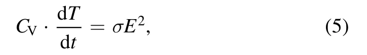
The current density of 106A cm-2and the concurrent heating associated with repetitive operation in HG GaAs PCSSs are the main causes of device destruction.Therefore,the thermal effect has a significant impact on the transient characteristics and longevity of PCSSs;the classic equation for thermal breakdown is

whereCVis the specific heat of the GaAs material,Tis the temperature of the GaAs PCSS,tis the optical pulse duration,κis the thermal conductivity of GaAs,σis the conductivity of GaAs,andEis the bias electric electric field.
In equation(4),the first left-hand term is the heat accumulated by the temperature increase in GaAs PCSS,the second left-hand term is the dissipated heat,and the righthand term is the Joule heat generated by the current.The excitation process can be regard as a transient and adiabatic process,in which the generated heat is much greater than the dissipated heat.Ignoring the dissipated heat,the equation for thermal breakdown can be expressed as
where all of the Joule heat generated by the current flowing in the plasma channel is considered to increase the temperature of the GaAs PCSS.The transport equation for the drift current is
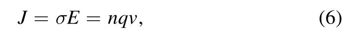
whereJis the current density in the plasma channel,nis the concentration of photoexcited carriers,qis the quantity of charge per carrier,andvis the average drift velocity of the photoexcited carriers.Combining equations(5)and(6),the equation for thermal breakdown is

Due to the high stability of the output waveform in a HG GaAs PCSS at a 1 kHz repetition rate,as shown in figure 4,it can be considered that the heat accumulation is identical for the excitation of each optical pulse.Therefore,the relationship between the temperature and the optical pulse duration can be shown as
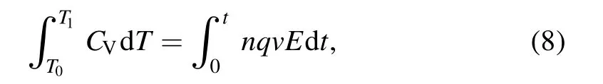
wheretis the optical pulse duration,T0is the room temperature(20°C),andT1is the temperature in the GaAs PCSS after heat accumulation.Therefore,the temperature increment is
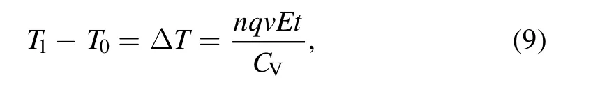
where ΔTis the increment of the temperature in the GaAs PCSS.
During repetitive operation,the longevity of the GaAs PCSS can be regarded as its operating time.Therefore,the heat effect can be calculated by the gradient of the temperature.Eventually,the gradient of the temperature(DT),which means the increment of the temperature in the GaAs PCSS at each time unit,is
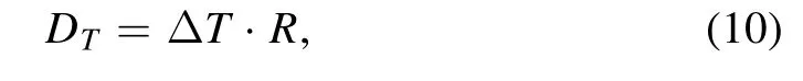
where R is the repetition rate of the optical excitation.
To analyze the damage caused by the heat effect in repetitive operation,the gradient of the temperature is calculated using equation(10).In our experiments,the material of the electrodes is an alloy of Au and Cr.The melting temperatures of Au and GaAs are 1064 °C and 1238 °C,respectively.However,the arsenic atoms begin to evaporate due to high vapor pressure at 620 °C,and the GaAs substrate will be invalid at that point.The repetition rate of the optical pulse and its duration are 1 kHz and 100 fs,respectively.In addition,the GaAs PCSS specific heat is 0.36 Jg-1K-1and the bias electric electric field is 10 kV cm-1.Moreover,the concentration of photoexcited carriers is 1016cm-3and considering that the mobility of electrons is greater than that of holes,the average drift velocity of the photoexcited carriers is set to 107cm s-1,which is the average saturated drift velocity of electrons.According to(10),the increment of the temperature per second is 44.50 K s-1.Consequently,ablation of the GaAs substrate and the electrodes occurs when the operational periods of the GaAs PCSS are 13.48 s and 23.50 s,respectively,which is consistent with the phenomenon of ablation observed in operation at a 1 kHz repetition rate.
4.Conclusions
GaAs is the optimum material with which to realize PCSS for transient switching,due to its carrier multiplication mechanism at low optical excitation energies.An interdigitated electrode structure is utilized to explore the photoexcited carrier dynamics under fs excitation at hundreds of nJ.Stable outputs are achieved for single-shot operation and 1 kHz operation with carrier multiplication.A Monte Carlo simulation is performed to demonstrate the interplay between the NDM effect and filamentary currents.It is shown that the bunched transport of photoexcited carriers produces a highdensity plasma channel of up to 106A cm-2.The maximum electric field near the anode is close to the intrinsic breakdown strength of the GaAs material.The concurrent heating is analyzed at a 1 kHz repetition rate,and the operation is considered to be an adiabatic process.The results show that melting of the GaAs substrate and electrodes in HG mode occur at 13.48 s and 23.50 s,respectively.This research provides a meaningful insight into the internal dynamics of GaAs PCSSs at low levels of optical excitation and characterizes thermal runaway in repetitive operation.
Acknowledgments
This work was supported in part by National Natural Science Foundation of China(Nos.51877177 and 52007152),in part by the Scientific Research Program Funded by Shaanxi Provincial Education Department(Nos.21JP085 and 21JP088)and the Youth Innovation Team of Shaanxi Universities,in part by the Natural Science Basic Research Plan of Shaanxi Province(Nos.2021JZ-48 and 2020JM-462),in part by Fellowship of China Postdoctoral Science Foundation(No.2021M702639),and in part by Open Research Fund of State Key Laboratory of Pulsed Power Laser Technology(No.SKL2020KF01).
ORCID iDs
猜你喜欢
杂志排行
Plasma Science and Technology的其它文章
- Characteristics of plasma in a novel laserassisted pulsed plasma thruster
- The effect of anode axial position on the performance of a miniaturized cylindrical Hall thruster with a cusp-type magnetic field
- Investigation into the thermal effect of the LIPS-200 ion thruster plume
- Early experimental investigation of the C12A7 hollow cathode fed on iodine
- Numerical study of the effect of aft-loaded magnetic field on multiple ionizations in Hall thruster
- Simulation of a helicon plasma source in a magnetoplasma rocket engine