Molecular dynamics study on mechanical behaviors of Ti/Ni nanolaminate with a pre-existing void
2022-07-26MengjiaSuQiongDengLantingLiuLianyangChenHeHeYinggangMiao
Mengjia Su,Qiong Deng,Lanting Liu,Lianyang Chen,He He,Yinggang Miao
Joint International Research Laboratory of Impact Dynamics and Its Engineering Applications,School of Aeronautics,Northwestern Polytechnical University,Xi'an,Shaanxi 710072,China
Keywords:Defective Ti/Ni nanolaminate Pre-existing void Interface Tensile behaviors Molecular dynamics
ABSTRACT Metallic nanolaminated materials possess excellent mechanical properties due to their unique modulation structures and interfacial properties.However,how microdefects affect their mechanical properties is still uncertain.To evaluate the influences of void location(in the crystalline layer and the Ti/Ni interface),void diameter(d) and thickness of the intermediate layer (h) on overall tensile behaviors,various types of defective Ti/Ni nanolaminates with pre-existing void are established by the molecular dynamics method in this work.The results indicate that the strength and plastic deformation mechanisms are strongly dependent on those determinants.Yield stresses of Ti/Ni nanolaminates decrease distinctly with increasing void diameter,while peak stresses with a void in the crystalline layer decrease with increasing d/h.Different void locations lead eventually to disparate initial plastic deformation carriers around the void,and various evolutions in the microstructure of the defective Ti/Ni nanolaminates.The Ti/Ni interface plays a significant role in the tensile process.The semi-coherent interface impedes new grains and lattice dislocations from passing across the interface,while the incoherent interface facilitates dislocations generating and sliding along the interface,and absorbs the dislocations moving to the interface.The results also indicate that the strain rate significantly affects the evolution of the microstructure and the tensile properties of defective Ti/Ni nanolaminates.
1.Introduction
Metallic nolaminated materials are kinds of two-dimensional materials synthesized by stacking their components alternately through physical or chemical methods.Metallic nanolaminated materials have received extensive attention from researchers due to their superior optical [1],electromagnetic [2,3] and reactive properties [4,5],which is ascribed to their special modulation structure and interfacial properties.Besides their remarkable physical and chemical properties,metallic nanolaminated materials also possess admirable mechanical properties[6–11].These excellent properties of metallic nanolaminates are strongly dependent on their special microstructures.Dense interphase interfaces can be formed between disparate crystals due to the differences in lattice structures.The interface can improve the strength of multilayered materials by hindering dislocations from passing through it.It can also reinforce the plastic properties by absorbing lattice dislocations and promoting the nucleation of interfacial dislocations[10,11].In summary,the interface functions as a bridge during the deformation and evolution of metallic nanolaminated materials.
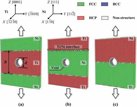
Fig.1.Schematic of Ti/Ni nanolaminates with pre-existing voids.
Apart from the abundant interfaces,there are also numerous defects induced by fabrication or mechanical deformation in the nanomaterials,including cracks,voids and other defects.Among these defects,the voids often exist as volume defects in the nanomaterials.Micro-voids or nanovoids can alter the mechanical behaviors of the nanomaterials,especially when the size of the void is at the same scale as the microstructure of the nanomaterial.Numerical simulations are powerful tools for solving the problems of extension and fracture of the defects.However,simulations based on continuous mechanics methods still have many challenges in solving the problems of the expansion and fracture of these defects.Thus,particle-based or multiscale algorithms are commonly used to solve the problem of the failure of these defects [12–18].The work from Timon Rabczuk's group proposed the multiscale framework and successfully used this approach in solving the problem of multiscale modeling and simulation of the fracture in solids.These multiscale algorithms were highly accurate in addressing failure events caused by extension of the crack,and their effectiveness has been verified at different scales.In addition,these multiscale methods or frameworks could be interfaced with other traditional numerical simulation software and had promising applications in future industries[12–14].The molecular dynamics(MD)method is another numerical method used to solve the problem of the propagation and failure of the defects at the atomic scale.With the assistance of MD methods and theoretical analysis,many researchers have attempted to probe the effect of defects,especially nano-voids,on the mechanical performance of nanomaterials.Among these efforts,much attention has been paid to the effect of size,and void propagation in different crystalline structures [15–18].Yang et al.discovered that stress concentration around the void was related to lack of necessary bonding atoms at the surface of the void,and the stress concentration was strongly dependent on the size and morphology of the void [15].Zhao et al.used the MD method to demonstrate that dislocations nucleating and emitting from the surface of the void caused premature yielding of the nanomaterials [16].The dislocation-based void growth mechanism had also been observed in the tensile testing of various defective face-centered cubic materials[17].In addition,there are numerous grain boundaries,twin boundaries and phase boundaries in nanomaterials.Interaction between the voids and these interfaces influences the overall properties of the nanomaterials.Zhang et al.fabricated different sizes of void in nano-twinned Cu to investigate its tensile behaviors and found that the voids did not reduce the strength of the material.On the contrary,resistance of the twin boundaries to the dislocations emitting from the surface of the void could enhance the mechanical performance[18].It is suggested from the above results that voids affect the strength and plastic deformation mechanisms of nanomaterials.
The introduction of voids,cracks and other defects into multilayered materials during fabrication is inevitable.Thus,the mechanical properties of the nanolaminates will be adversely affected,and the interaction between defects and interfaces may cause a transition in the plastic deformation mechanisms of the nanolaminated materials.However,little literature has focused on the voids in nanolaminated materials.Shang et al.attempted to explore the influence of the interfacial void on the mechanical properties of defective Ni/Ni3Al nanolaminates.When the diameter of the void was small,the yield stress of the defective nanolaminate would be higher than that of the perfect sample,which was related to the fact that the small-sized void ameliorated the concentration of local energy around the interfacial regions.However,the yield strength showed a significant decline with the increasing of the diameter,which was attributed to the transition of the plastic deformation.And the intrinsic mechanism varied from edge dislocations emitting at the interface to partial dislocations arising from void surfaces[19].However,it is still doubtful whether similar conclusions could be applied to other types of nanolaminated materials.For the nanolaminates containing disparate crystalline components,the plastic deformation mechanisms are different for different crystalline structures,and the interaction between different plastic deformation carriers and defects will be more complex.For example,it has been proven that the main plastic deformation carriers are quite different in disparate crystalline structures of Ti/Ni (hexagonal close-packed/face-centered cubic,HCP/FCC) nanolaminates[20].For nanolaminates with different crystals,how do voids affect the overall properties of the materials?How do voids interact with interfaces and various plastic deformation carriers? Also,what roles do heterogeneous interfaces play in the deformation of the nanocomposites?These questions need to be addressed urgently to gain a more comprehensive understanding of the mechanical evolution of these nanolaminated materials.Therefore,the MD method is employed to evaluate the influence of the pre-existing void on defective Ti/Ni nanolaminates during tensile loading.The results obtained from this work could further enrich the theoretical and experimental research of metallic nanolaminated materials.
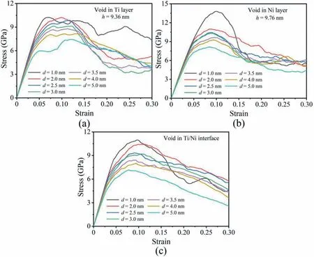
Fig.2.Stress-strain curves of different Ti/Ni nanolaminates,(a)Model I,the void is in the Ti layer,(b)Model II,the void is in the Ni layer,(c)Model III,the void is in the Ti/Ni interface.
2.Methods
The schematic of a Ti/Ni nanolaminate with a pre-existing void is shown in Fig.1.In this work,to find how the location of a void impacts the tensile behaviors of a nanocomposite,voids are prefabricated at the internal Ti layer,Ni layer,and Ti/Ni interface,respectively.The dimensions of all samples are selected as2.99×16.86×19.12 nm3.For the first two models,the thickness of the crystalline layer is designed to meet the scale requirements:2hNi=hTiorhNi=2hTi,while the layer thickness ishNi=hTifor the third model.That is to say,the modulation ratios of the Ti/Ni nanolaminates are fixed as η=1:1.In addition,void diameters(d)are selected from 1.0 to 5.0 nm for all models to show the influence of the variation of void diameter on the tensile properties of defective nanolaminates.The thicknesshis constant for the first two models.The initial crystalline orientations of different phases are shown at the top of Fig.1.
The Ti{0001} and Ni{111} planes for respective crystals are chosen perpendicular to the loading direction,as the atoms could attain a more stable state at close-packed planes during the vapor deposition [21,22].The semi-coherent Ti/Ni interface is formed between two components due to the disparate crystalline structures and lattice parameters of the two phases,as shown in the dotted rectangle of Fig.1.Periodic boundary conditions (PBCs) are applied in all directions of the defective Ti/Ni nanolaminates to eliminate the boundary effect and focus only on the interaction between voids and interfaces.
Interaction potential is vital for the accuracy of the MD simulation.The embedded atom method (EAM) [23,24] and modified embedded atom method (MEAM) [25,26] potentials can be used to describe the atomic interactions in Ti–Ni binary systems.The MEAM potential is suitable to predict martensitic phase transitions and thermodynamic behaviors of TiNi alloys [25,26],while the EAM potential [23,24] is suitable to predict the properties of metallic multilayered materials prepared by vapor deposition,and has been widely used to predict the mechanical behaviors of Ni/Cu [27],Cu/Ag [28],Ti/Al [29,30] and Ti/Ni[31]nanolaminated materials.Thus,the EAM potential integrated by Zhou and Wadley was employed to describe the interactions between Ti–Ti,Ti–Ni and Ni–Ni atoms.The timestep is kept as 3 fs(fs,10-15s)for all simulations.The Velocity-Verlet integral algorithm is employed to calculate the velocity and positions of the simulated atoms.Before loading is applied to the models,all defective nanolaminates are first equilibrated at zero pressure and 0.01 K for 90 ps(ps,10-12s)to attain a stable state.Then,tension loading along the Z-direction is applied by stretching the Newton atoms with a constant strain rate of 3.3×10⁸S-1,and the total tensile strain is set as 0.3.The atomic stress is solved by the Viral theorem [32] in this work.After the calculation,most post-processing work is conducted through Open Visualization Tool(OVITO) [33],as plenty of analysis modules are integrated in the software.The common neighbor analysis (CNA) method is employed to identify different crystalline structures and defects[34].Crystalline and non-structure atoms are rendered in different colors,as indicated in the top of Fig.1.Different dislocations in specific crystalline structures are analyzed by the dislocation extraction(DXA)method[35].
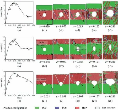
Fig.3.Atomic configurations of defective Ti/Ni nanolaminates at the specific tensile strain,(a)Model I,the void is in the Ti layer,(b)Model II,the void is in the Ni layer,(c) Model III,the void is in the Ti/Ni interface.
3.Results
3.1.Stress-strain curves
The stress-strain curves of different types of defective Ti/Ni nanolaminates are shown in Fig.2.It is found that with increasing the tensile loading,the stress-strain curves of all models show a linear relationship,where the nanolaminates deform elastically in this stage.After the elastic stage,the stresses of the three models increase with the increasing strain until reaching the maximum value,which indicates the occurrence of plastic deformation.Thereafter,the stresses of the first two models first decrease and then fluctuate slightly with the increasing tensile strain.However,the stresses of the third model always decrease with the increasing tensile strain.Yield stress and peak stress are selected to quantitatively assess the influences of void size on the tensile properties in this part.According to the obtained stress-strain curves,yield stress is known as the stress value at the end of the linear stage of the curves,while maximum value is usually defined as peak stress.As shown in Fig.2,both the yield stress and the peak stress of all models gradually drop with the increasing void diameter.Model II possesses maximum strength among those nanolaminates when the void size is the same,which denotes the Ni layer is the hard phase in Ti/Ni nanolaminates.In addition,the stress-strain curves show different characteristics when the voids are in different locations,which implies different microstructure evolutions of disparate defective Ti/Ni nanolaminates.The specific atomic configuration evolutions will be presented in Section 3.2.It is observed from Fig.2 that not only do void location and void diameter significantly affect the tensile strength of defective Ti/Ni nanolaminates,they also alter the plastic behaviors of the materials.
3.2.Microstructure evolution
Fig.3 depicts the microstructure evolution of three defective Ti/Ni nanolaminates;corresponding stress-strain curves are shown in the left inset.Only models with a void diameter of 3 nm are shown in Fig.3,which aims to show the disparate plastic deformation mechanisms of defective Ti/Ni nanolaminates.For Model I,plastic deformation initially arises from the void at ε=0.039,which corresponds to the point al of the stress-strain curve.When the tensile strain is lower than 0.039,the stress increases linearly with the increase of the applied strain,and the sample deforms elastically during the initial stretching process.Plastic deformation begins to arise in the Ti layer once the strain is above 0.039,and the relationship between stress and strain becomes nonlinear.Therefore,0.039 is defined as the yield strain for Model I,and the corresponding stress is defined as the yield stress.Obviously,the yield stress of Model I is strongly related to the plastic deformation around the void.As shown in Fig.3(a1),slip bands initially arise from the surface of the void and slide along the prismatic planes of the Ti layer.Due to the finite slip systems in HCP-based material,the dislocation movement in the Ti layer is hard to activate at this loading condition.Consequently,slip bands initially generate at the surface of the void [36].The slip bands grow quickly under tension loading,but are subsequently hindered by the Ti/Ni interfaces.Meanwhile,new grains germinate and propagate from the tip of the slip bands,shown as the black circle in Fig.3(a2).Thereafter,these new slip bands continuously emit from the void,and grow quickly with the increasing tensile strain,while the Ni layer always deforms elastically under tension loading.When the tensile strain is 0.083,some slip bands propagating along a certain direction reach the interface,which leads to a great change in the interfacial structure.It can also be discovered from Fig.3(a3)that some partial dislocations germinating at the interfacial regions start to propagate in the Ni lattice.As shown in the stress-strain curve,the maximum stress (or peak stress) is also obtained atε=0.083.Thus,for Model I,the peak stress is related to the slip bands passing through the interface.For a larger strain,the growth of new grains in the Ti layer is impeded by the interface,and the new grains start to expand parallel to the interface.Moreover,the new grains rotate into a new direction,which is quite different from the initial grain orientation of the parent phase.And the atomic configuration in the Ti layer exhibits a polycrystalline trend under the tension loading.The grain reorientation has also been observed in the simulation [29,37,38] and experiments [39,40] of various HCP-based metals.In obstructing and absorbing the different lattice defects,the semi-coherent interface gradually becomes incoherent,which stimulates the proliferation of partial dislocations with Burgers vector of b=1/6 [112]in the Ni layer.The new grains occupy the entire Ti layer,further enhancing the tension loading.After that,basal dislocations withb=begin to emit from the surface of the void,which leads to the accumulation of FCC stacking faults around the void.As can be seen from Fig.3(a),the area of the void in the Ti layer is increasing under the external loading.
For Model II,the Ti/Ni nanolaminate first yields at ε=0.048.As shown in Fig.3(b1),one dislocation withb=1/6 [112]first nucleates from the surface of the void and slides along the {111} plane in the Ni layer.Subsequently,the sliding dislocation is impeded by the Ti/Ni interface.Absorbing the partial dislocations leads to a great change in the stress distribution at the interface,and the plastic deformation in the Ti layer is activated at this moment.Different plastic deformation carriers start to evolve from the interfacial regions and interact with each other in the Ti lattice,such as the movement of slip bands,the expansion of new grains and allotropic phase transformation.As for the Ni layer,deformation twins arise from the void as the result of trailing dislocations nucleating from the void slide along the adjacent plane of leading dislocations[30,41].For the larger strain,the new grains occupy the whole Ti layer,and numerous partial dislocations continually generate at incoherent interfaces and slide in the Ni layer.It can be discovered from Fig.3(b)that the void extends along the loading direction and becomes narrower with the increasing tension loading.
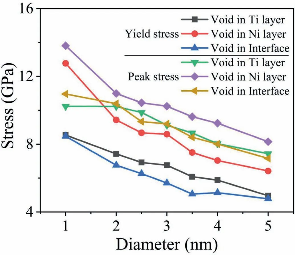
Fig.4.Tensile strength of defective Ti/Ni nanolaminates.
For Model III,the slip bands initially generate at the junction of the void and the interface,and propagate along specific directions at the internal Ti layer.Some partial dislocations emit from the interface and slide in the Ni layer at ε=0.105.After that,the grain reorientation in the Ti layer dominates the main plastic deformation;it also accompanies the dislocation sliding in the Ni layer.Interestingly,the void in the Ti layer expands with the increasing tension loading,while the void in the Ni layer seems to be unchanged during the tensile process.Combining the analysis from Figs.2 and 3,the variation of the location of the void in the crystalline layer or the interface not only causes a difference in the tensile properties of the samples,it also alters the initial plastic deformation carriers,which eventually results in quite different plastic deformation mechanisms of the defective Ti/Ni nanolaminates.We have also simulated the tensile behaviors of same-sized Ti/Ni nanolaminates with asymmetric void location in the Supplementary Materials.The results indicate that variation of the relative position between the void and the interface influences the yield and peak stress of the defective Ti/Ni nanolaminates,but plays only a small role in the plastic deformation mechanisms of the defective samples.The transition of the plastic deformation mechanism is dependent only on the void locating in a different lattice(either in the Ti or Ni lattice)or interface.
4.Discussion
4.1.Effect of voids on the tensile strength of Ti/Ni nanolaminates
It can be seen from Fig.3 that the yield stress of defective nanolaminate is connected with the plastic deformations around the void,and the peak stress is dependent on the interplay between Ti/Ni interface and different plastic deformation carriers sprouting at the crystalline layer.Fig.4 describes the relationship between the strength and void diameter of different models.The yield stress and peak stress of Model II are larger than these of the other models at the same void size,while the strength from Model I is close to that of Model III at the same condition.This could be because the Ni layer is a hard phase in the Ti/Ni nanolaminate,and thus the driving force for further plastic deformation in the Ni layer requires much more external stress,while the plastic deformations for the other two models occur mainly in the Ti layer,which results in the subequal strength of these models.
As shown in Fig.4,the yield stress and peak stress of the defective Ti/Ni nanolaminates show a descending trend with an increasing void diameter.The size effect of the yield stress is ascribed to the stress being concentrated on the surface of the void [15].To show the underlying mechanisms,the stress distribution along the Z-direction of different nanolaminates after equilibration is presented in Fig.5.Atoms in the surface of the void are in a high stress state due to lack of bonding atoms,so the defective nanolaminate first yield at the void.There are more atoms in the high stress state at the surface of the void for the larger void diameter.Thus,smaller applied stress is required for further plastic deformation.The equivalent area perpendicular to the loading direction decreases with the increasing void diameter,which can lead to an increase in the proportion of atoms with high stress.
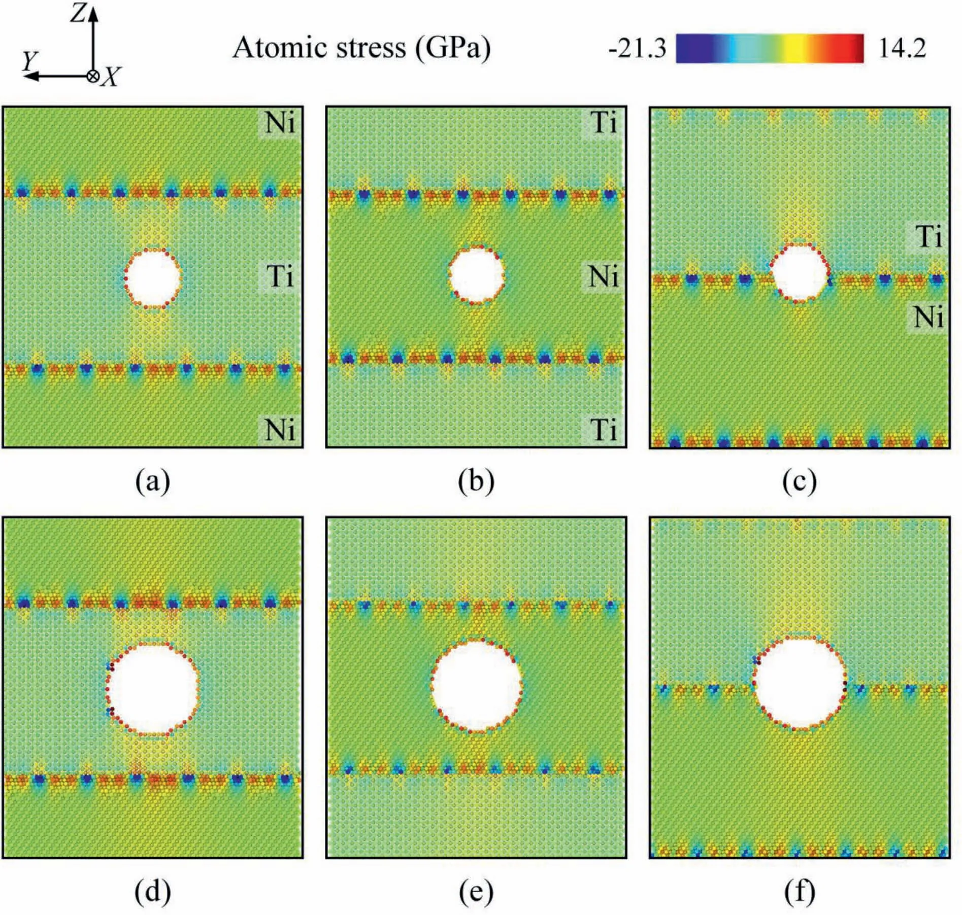
Fig.5.Atomic stress distribution along the Z-direction of different Ti/Ni nanolaminates after equilibration,(a)and(d)Model I,the void is in the Ti layer,(b)and(e)Model II,the void is in the Ni layer,(c)and(f)Model III,the void is in the Ti/Ni interface.(a)–(c)The diameter of the void is 3 nm,(d)–(f)the diameter of the void is 5 nm.
As indicated from the evolution of the microstructure,the size effect of peak stress is strongly dependent on the void and interface for the first two models.When the thickness of the intermediate layer is the same,the sample with larger void diameter possesses more atoms in a high stress state at the region between the interface and the void.Therefore,less external stress is needed to induce the interaction between the Ti/Ni interface and different plastic deformation carriers of the crystalline layer.As for Model III,higher stress concentrates at the junction of the void and the interface.Increasing the void diameter means decreasing the effective area perpendicular to the loading direction.Dislocations and deformation twinning are more likely to nucleate and interact with the interface.Thus,the size effect can also be observed for the model with the void in the Ti/Ni interface.According to the above analysis,the strength of the defective nanolaminate is strongly connected with the location of the void.Furthermore,the size effect of yield stress is only dependent on the void diameterd.For models with a void in the crystalline layer,the size effect of peak stress is determined by the void diameterdand the thickness of the intermediate layerh.
4.2.Coupled effect on the peak stress of defective Ti/Ni nanolaminates
Some other defective models are established with voids in crystalline layers to further explore the relationship between peak stress and characteristic parameters of defective Ti/Ni nanolaminates.The schematic of newly established Ti/Ni nanolaminates is shown in the lower left corner of Fig.6.The void diameter is fixed as 3 nm,and various intermediate layer thicknesses are selected to seize the main factors for peak stress.This established model will be named sample 2(S2)to distinguish it from the sample (S1) in the previous section.It is noted that the selected intermediate layer thickness in S2 is maintained to be samed/has the value in S1.
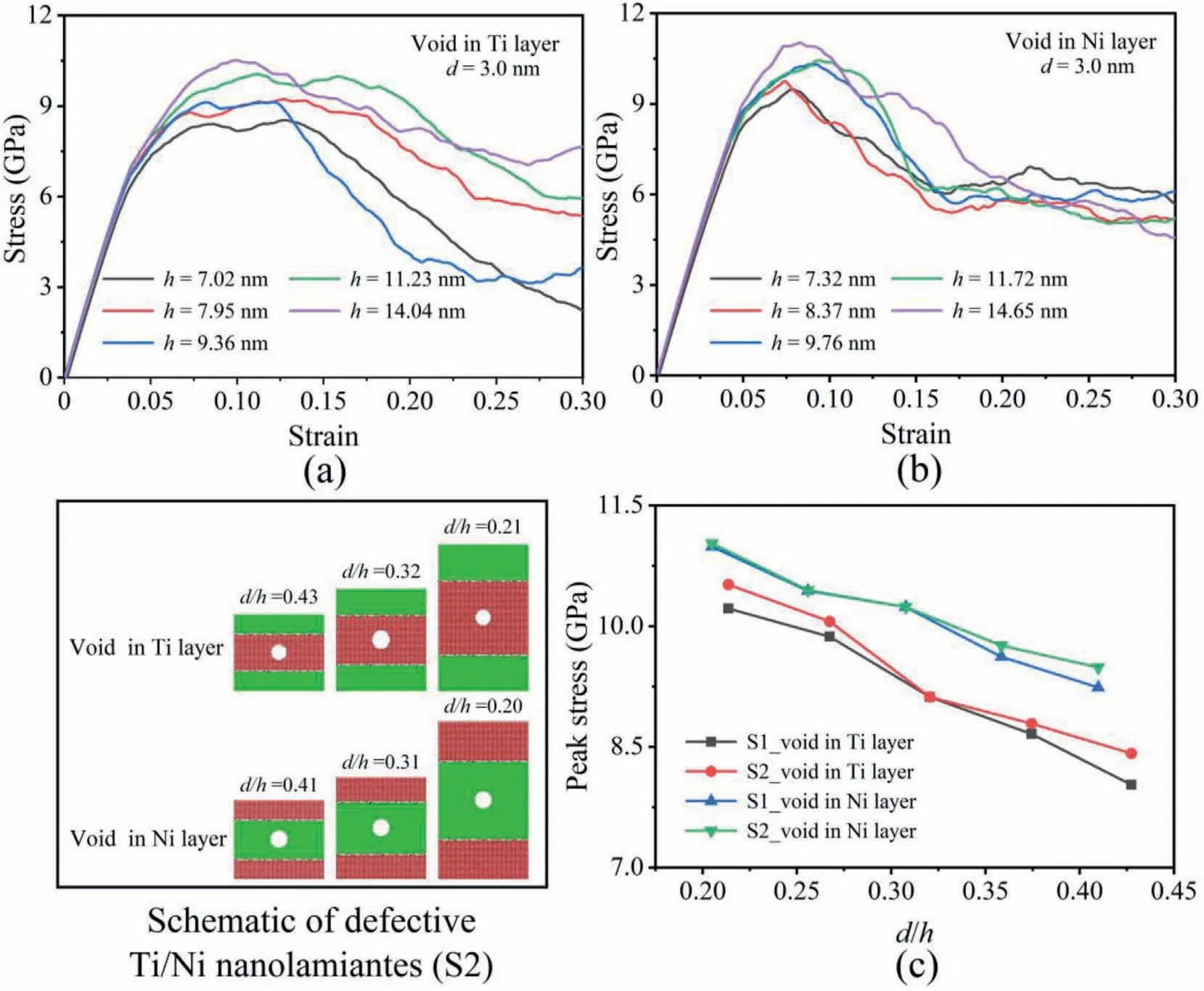
Fig.6.Tensile properties of different types of defective Ti/Ni nanolaminates,(a) Sample 2,the void is in the Ti layer,(b) Sample 2,the void is in the Ni layer,(c)relationship between peak stress and d/h. The schematic of defective Ti/Ni nanolaminates with different d/h values are shown in the lower left corner of the figure.
The stress-strain curves of S2 are depicted in Fig.6(a)and(b),which show a similar tendency as the stress-strain curves in Fig.3(a) and (b).The yield stresses of the defective samples in S2 are almost the same,which is close to the value of the sample withd=3 nm in S1.It is verified that the yield stress of defective Ti/Ni nanolaminate is only dependent on the void diameter.However,the peak stress in S2 decreases with the decrease in the thickness of the intermediate layer.Namely,peak stress is positively correlated with the thickness of the intermediate layer when the void diameter remains constant.However,with respect to S1,the peak stress is negatively correlated with the void diameter when the thickness of the intermediate layer is fixed.Combining both observations,a more meaningful parameter,i.e.,d/h,is selected to evaluate the peak stress of the defective nanolaminates.The relationships between peak stress andd/hof various defective Ti/Ni nanolaminates are presented in Fig.6(c).The peak stresses of all models are inversely proportional to the value ofd/h.The peak stresses for different samples are very close at the samed/h,whether the void is in the Ti or the Ni layer.The result can be explained by the stress distribution of the defective Ti/Ni nanolaminates in Fig.5.When the void diameter is smaller or the thickness of the intermediate layer is larger,the area between the void and the interface is larger,which can alleviate the concentration of stress at the intermediate layer.Therefore,more stress is required to drive different plastic deformation carriers to propagate across the interface,so that the model possesses a larger peak stress.When the value ofd/htends to be zero,the peak stress of the defective Ti/Ni nanolaminate can approach the maximum value,i.e.,the peak stress of the perfect Ti/Ni nanolaminate.Therefore,the peak stress of the defective nanolaminate depends on the void diameter and the thickness of the intermediate layer,and the value is inversely proportional tod/h.
4.3.Strain rate effect on the tensile behaviors of defective Ti/Ni nanolaminates
Besides the internal microstructural parameters,the external strain rate also significantly affects the mechanical responses of the defective Ti/Ni nanolaminates.This section will focus on the role of the strain rate during the tensile process of the defective samples.Strain rates from 6.6×10⁸s-1to 3.3×10⁹s-1are used to verify the influence of strain rate on the tensile strength of the nanolaminates.The models in this section are consistent with the dimensions in Fig.3,i.e.,the void diameter is fixed as 3 nm for all the defective models.The stress-strain curves of the Ti/Ni nanolaminates at different strain rates are plotted in Fig.7.As shown in Fig.7(a) to 7(c),the stress-strain curves of all samples exhibit two different trends in the selected ranges of the strain rate.After the initial elastic stage,the stress for 6.6×10⁸s-1is slightly higher than the value for 3.3×10⁸s-1at the same tensile strain.However,once the strain rate increases over 1.0× 10⁹s-1,the stress shows a remarkable increase compared with the stress at the former two strain rates.This phenomenon implies the mutation of plastic deformation mechanisms at the selected strain rate.Searching more details of the stress-strain curves,the yield stress and peak stress of different types of Ti/Ni nanolaminates are displayed in Fig.7(d).Both of these parameters increase with increasing the applied strain rate.However,the peak stresses present a significant increase when the strain rate is above 1.0×10⁹s-1,and,for all defective nanolaminates,reach a plateau with further increasing the strain rate.
For further investigation into the influence of the strain rate on the tensile behaviors of defective Ti/Ni nanolaminates,the atomic configurations are presented with different types of defective Ti/Ni nanolaminates under various strain rates in Fig.8.The microstructures of different samples at different yield strains are shown in Fig.8(a)to 8(d).It can be seen that the number of plastic deformation carriers emitting from the surface of the void increases with the strain rate for all samples.At higher strain rates,more plastic deformation carriers may be activated per unit time,and greater applied stress is required to drive these plastic deformation carriers.Consequently,the yield stresses of defective Ti/Ni nanolaminates show a positive correlation with the applied strain rate.
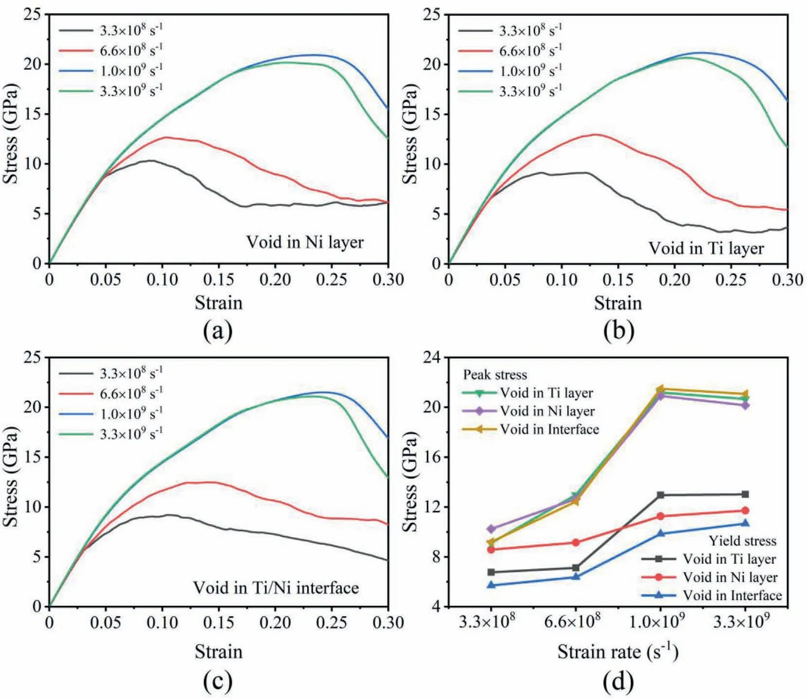
Fig.7.Tensile properties of defective Ti/Ni nanolaminates under different strain rates.(a)Stress-strain curves of Ti/Ni nanolaminates with the void in the Ti layer,(b)Stress-strain curves of Ti/Ni nanolaminates with the void in the Ni layer,(c)Stress-strain curves of Ti/Ni nanolaminates with the void in the Ti/Ni interface,(d)Yield and peak stresses of different types of defective Ti/Ni nanolaminates under different strain rates.
The atomic configurations of the defective samples at peak strain are more complex at different strain rates.When the strain rate is below 1.0×10⁹s-1,the number of plastic deformation carriers in the crystalline layers increases with the strain rate.Once the strain rate is above 1.0× 10⁹s-1,amorphization of the crystalline structures is observed around the interface,in addition to the different plastic deformation carriers in the crystalline phase.The amorphization leads to the appearance of sub-voids in the interfacial regions and the destruction of interfacial structures,which contributes to the significant descending trend of the stress-strain curve at the high strain rate after reaching the peak value.From the above analysis,it can be seen that the evolution of the microstructure and the tensile properties of the defective Ti/Ni nanolaminates are closely related to the external strain rate.The yield stress increases with the increase of the strain rate,while the peak stress increases with increasing strain rate,and reaches a plateau as the strain rate increases higher than 1.0×10⁹s-1.The evolution of the microstructure also shows that local amorphization occurs at the interfacial region when the strain rate is over 1.0×10⁹s-1.
4.4.Role of the interface during the tensile process
Dense interfaces exist in multilayered materials,which not only can affect the strength of the materials,but which also play a significant role in the plastic properties for different types of nanolaminates.Generally,interfaces in multilayered materials can play the same role as grain boundaries in polycrystalline material under applied loading.Previous study on polycrystalline high-entropy alloys(HEAs)indicates that partial dislocations can arise from grain boundaries and also can be absorbed by the opposite grain boundaries.And for the small-sized polycrystalline HEAs,plasticity can be achieved through the rotation of interior grains and the migration of grain boundaries [42].Similarly,interfaces in nanolaminated materials can also serve as dislocation sources and sinks during the plastic deformation.Hindering the propogation of dislocations across the interface can enhance the strength of nanolaminated materials [11].When the layer thickness of the crystalline phase is inadequate to nucleate dislocations,the plastic defamation can be dominated by the interface rotation [31,43].However,there are some differences between grain boundaries and interfaces.Grain boundaries usually exhibit disordered structures in polycrystalline materials,while interfaces can be divided into coherent,semi-coherent and incoherent interfaces with the increasing degree of mismatch.Atoms in coherent and semi-coherent interfaces show a regular distribution,while they are in a disorderly arrangement in most of the incoherent interfaces.Complex stress distribution on the interfaces makes interfacial dislocations and twin embryos easily nucleate from the interfaces.Meanwhile,plastic deformation of the interface itself can connect the disparate plastic deformation carriers of the adjacent components,and guarantees larger plastic deformation ability of the multilayered composites[10,11].
For further investigation into the role of the interface in the tensile behaviors of defective Ti/Ni nanolaminates,Fig.9 describes the interaction between the interface and different plastic deformation carriers emitting from the void during the tensile process.The snapshots in Fig.9 are local enlarged details of the atomic configurations for three models at the respective tensile strains.Due to differences in crystalline structures,plastic deformation carriers in the Ti or Ni layer cannot pass through the interfaces directly,and the plastic deformation in disparate crystals is bridged with the assistance of interface plasticity.
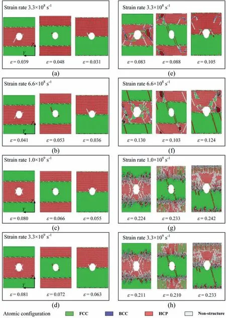
Fig.8.Atomic configurations of different types of defective Ti/Ni nanolaminates under various strain rates.(a)–(d)Atomic configurations at the yield strains.(e)–(h)Atomic configurations at the peak strains.
As shown in Fig.9(a),the initial slip band slides along theplane in the Ti layer and is impeded and absorbed by the interface at ε=0.046,which also leads to the transformation of the local semicoherent interface into incoherent regions.However,once the 1.0×10⁹s-1slip band reaches the interface and is absorbed by the interface,the partial dislocation with Burgers vector of b=1/6 [112]can nucleate from the interface and propagate in the Ni layer at ε=0.083.For the larger strain,hindering the expansion of the new grain causes further destruction of the semi-coherent interface.Thus,different types of dislocations can be generated from the incoherent interface and slide along certain planes in the Ni layer.
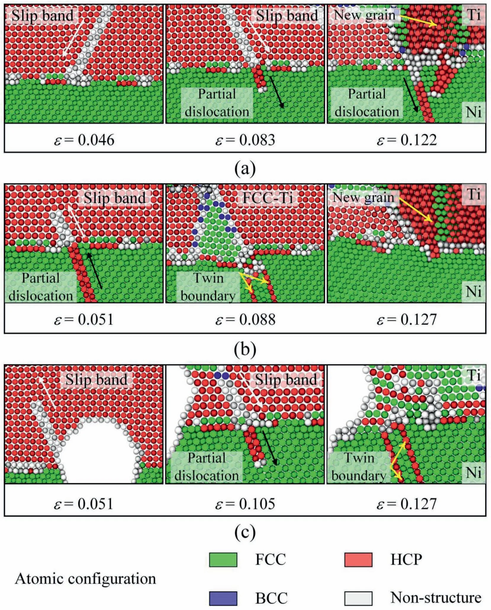
Fig.9.Interaction between the Ti/Ni interface and different plastic deformation carriers emitting from the void.(a)Model I,the void is in the Ti layer,(b)Model II,the void is in the Ni layer,(c) Model III,the void is in the Ti/Ni interface.
For the second model,the incoming partial dislocation is absorbed by the Ti/Ni interface,then the slip band can be activated and slides along the plane in the Ti layer at ε=0.051,as shown in Fig.9(b).The trailing dislocations continually arise from the surface of the void and are absorbed by the Ti/Ni interface with increasing tensile strain,which leads to step structures on the Ti/Ni interface and phase transformation in the opposite Ti layer.Deformation twinning can be observed in the Ni layer as a consequence of the trailing partial dislocations sliding along the adjacent plane of the leading dislocation.Similarly,the semicoherent interface becomes incoherent due to the absorption of incoming grain boundaries.For the model with a void in the interface,the first slip band arises at the junction of the interface and the void.Different plastic deformation carriers in respective crystalline structures can also be connected with the assistance of the Ti/Ni interface with increasing tensile strain,as shown in Fig.9(c).
Fig.10 further depicts the interfacial structure evolutions of the lower interface in Model I,with the aim of assessing how the interface affects the plastic deformation of the defective nanolaminates.For the case where the crystalline structures and lattice parameters are different between two metals,mismatch dislocations are easily formed to balance the lattice distortion around the interfacial regions.As shown in Fig.10(a),the formation of misfit dislocation networks leads to an alternate distribution of HCP and FCC atoms at the Ti/Ni interface.When the plastic deformation carriers have not evolved into the interface,the interface only sustains elastic deformation and maintains regular distribution.As the loading continues,the initial misfit dislocation networks are destroyed when the slip bands reach the interface.The local regions of the interface gradually transform into incoherent regions,which results in a stress concentration on the incoherent regions,as shown in Fig.10(b).At this moment,the semi-coherent interface can still impede different plastic deformation carriers from passing through the interface,while the stress concentration at the incoherent regions can promote the nucleation of the interfacial dislocations.The misfit dislocation networks are destroyed completely as they continually impede and absorb incoming plastic deformation carriers from the Ti and Ni layer.Consequently,the semi-coherent interface thoroughly transforms into the incoherent interface.Due to the incoherent interface continually impeding and absorbing dislocations,the initial flat interface transforms into a rugged one eventually,as shown in Fig.10(d).
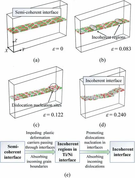
Fig.10.Atomic configurations of the Ti/Ni interface during the tensile process.
In summary,the interface plays an important role in the tensile process of Ti/Ni nanolaminates.As shown in Fig.10(e),the semi-coherent interface hinders different plastic deformation carriers from crossing the interface.Impediment and absorption of the incoming carriers causes the semi-coherent interface to transform into an incoherent interface.The incoherent interface can stimulate plastic deformation around the interfacial regions and promote the absorption of the different lattice defects generating from the crystalline phases.
5.Conclusions
In this work,the molecular dynamic method is employed to probe the influence of void location,void diameter and the thickness of the intermediate layer on the mechanical properties of defective Ti/Ni nanolaminates.The results indicate that strength and plastic deformation mechanisms of the materials are strongly dependent on those factors.Some conclusions are summarized as follows:
(1) The strength of defective Ti/Ni nanolaminates is dependent on the void locations,the void diameter (d) and the thickness of the intermediate layer (h).Yield stress is only determined by void diameter,and decreases with increasing void diameter.Peak stress in the crystalline layer is dominated by the thickness of the intermediate layer and the void diameter,and the value is inversely proportional tod/h.
(2) Plastic behaviors of defective nanolaminates are strongly linked with void locations.When the void is in the Ti layer,slip bands first arise from the surface of the void and propagate at the internal layer,which eventually leads to grain reorientation in the Ti layer.For voids in the Ni layer,the nucleating and propagating of partial dislocations in the Ni layer causes the formation of deformation twins around the void.For the case of the void locating at the interface,the slip bands are initially activated at the junction of the void and the interface,then the propagation of partial dislocations in the Ni layer is stimulated both in the surface of the void and in the interface.Among different defective samples,the void in the Ti layer is more likely to expand under external loading.
(3) The loading strain rate also significantly affects the evolution of the microstructure and the tensile properties of defective Ti/Ni nanolaminates.The yield stress increases with the increasing strain rate,while the peak stress increases with the increasing strain rate,and reaches a plateau as the strain rate is greater than1.0×109s-1.The evolution of the microstructure also shows that local amorphization occurs at the interfacial region when the strain rate is above1.0×109s-1.
(4) The Ti/Ni interface is crucial for the plastic deformation of the nanolaminates.The initial semi-coherent interface impedes incoming plastic deformation carriers from passing through the interface.However,the semi-coherent interface gradually turns into an incoherent interface due to impeding and absorbing the different deformation carriers.The incoherent interface can drive plastic deformation around the interfacial regions and promote the absorption of the various lattice defects generating from the crystalline phases.
Declaration of competing interest
None.
Acknowledgments
This work is supported by the National Natural Science Foundation of China(Grant No.12072286),the Natural Science Foundation of Shaanxi Province (No.2020JM-095 and 2021JM-045) and Fundamental Research Funds for the Central Universities(No.G2020KY05112).
Appendix A.Supplementary data
Supplementary data to this article can be found online at https://doi.org/10.1016/j.nanoms.2021.07.010.
杂志排行
Namo Materials Science的其它文章
- Preface of “Trends in Nanomaterials and Nanocomposites:Fundamentals,Modelling and Applications”
--Festschrift in honor of Prof Yiu-Wing Mai's 75th birthday - A comparative study of 85 hyperelastic constitutive models for both unfilled rubber and highly filled rubber nanocomposite material
- On mechanical properties of nanocomposite hydrogels:Searching for superior properties
- Ultra-transparent nanostructured coatings via flow-induced one-step coassembly
- VN nanoparticle-assembled hollow microspheres/N-doped carbon nanofibers:An anode material for superior potassium storage
- Core-shell structured silk Fibroin/PVDF piezoelectric nanofibers for energy harvesting and self-powered sensing
