Energy Storage Mechanism of Vanadium Nitride via Intercalating Different Atomic Radius for Expanding Interplanar Spacing
2022-07-04YingLiuLingyangLiuLongKangandFenRan
Ying Liu, Lingyang Liu , Long Kang, and Fen Ran*
1. Introduction
In order to maintain the economic growth of modern society while protecting the earth’s environment, there is an urgent need to increase the utilization of renewable clean energy from nature, such as solar energy, wind power, geothermal energy and tidal energy.[1–3]Therefore, efficient intermediate devices for energy storage and release are essential.As the most important supplement to the already commercialized lithium-ion battery, supercapacitors (SCs) have received great attention because of their rapid charge and discharge, high efficiency and robust cycle ability.[4–7]In the field of SCs, the most promising research is the practical application of electrode materials. And in this case,metal nitride has received increasing attention due to its fast electron transfer and large energy storage capability.[8–10]In particular,vanadium nitride (VN), as a typical pseudocapacitive anode material, has a wide operation potential (0 V to −1.2 V) and high theoretical specific capacitance (1350 F g−1), which is even higher than that of RuO2.However,some reported high values were usually tested with a very low mass loading (0.2 mg) and at a low sweep rate (2 mV s−1).[11]Therefore, it is particularly important to study its energy storage mechanism to further improve its capacitance in practical applications. To date, as one of the most important pseudocapacitive anode materials,the energy storage mechanism has not been completely united. Although VN has been widely studied, the reaction mechanism during charge and discharge is still in the theoretical guessing stage, and the most widely accepted theory reaction is as follow:

In this equation, VNxOy||OH−represents the forming of electrical double layer and VNxOy-OH means the Faraday reaction between OH−and VNxOy. It can be seen that both are directly related with hydroxyl ions adsorbed on “non-specific sites”.[11–13]Some previous reported articles attempted to explain the reaction mechanism of VN under completely anaerobic reaction conditions,and even pure phase VN materials were prepared without considering the cost, but the samples were still“slightly oxidized”.[14]Scientific research needs theoretical support under ideal conditions,but the ultimate goal is to serve the actual application.However,it is usually extremely hard to achieve the ideal conditions in practical applications. For example, oxygen widely exists in aqueous electrolyte and in air.
Taking into account the actual situation,in this article,based on the research and popularization of VN-based active material properties under conventional and non-extreme conditions, we intended to provide a meaningful guidance in the performance improvement and practical applications of VN materials. We studied the hydroxyl adsorption energy and adsorption sites (“non-specific sites”) by means of Density Functional Theory (DFT). And we found that OH−must be absorbed on V atoms, which means that O element maybe is not the key to improve the electrochemical performance.[15–17]Based on this consideration, we designed a series of microscopic ordered structure anion vanadium metal organic frameworks (V-MOFs) precursors containing impurity atoms (C atoms and S atoms) in order to prepare ordered impurity atoms doped VN theoretically. Through this method with adding other impurity atoms to enlarge the interplanar spacing,the energy storage mechanism of vanadium nitride can be studied,and DFT is used to further prove the obtained results.
2. Results and Discussion
Our overall design idea is presented in Scheme 1. The material structure of traditional cationic V-MOFs,which is based on organic ligands,will collapse after annealing,and finally the basic purpose of long-range order retainment can’t be achieved. Previous studies have stated that long-range ordered structures play a crucial role in maintaining electron conductivity and improving the electrochemical properties.[10,18–20]Based on these considerations, we firstly attempted to synthesize two kinds of one-dimensional anion grafted V-MOFs precursors,and further successfully prepared VN materials to study the relevant mechanisms under such favorable conditions. The synthesized anionic V-MOFs are classified into two types according to different kinds of organic amines.These two organic amines will have different impurity atoms after pyrolysis. P-phenylenediamine (PPD) will only retain C impurity atoms, while 2, 5-diaminobenzenesulfonic acid (BSA) can retain both C and S impurity atoms, thus further controlling the impurities in the final product VN.This means that the VN-C was obtained from PPD-VMOFs (V-MOFs-C) and the VN-C-S was obtained from BSA-V-MOFs(V-MOFs-C-S)(Scheme 1).Two types of anionic V-MOFs were synthesized through the hydrothermal synthesis method. Organic amine cation (OAM+) and metavanadate anion (VO-3) were coordinated together to form linear anionic V-MOFs (Figure S1, Supporting Information). The one-dimensional structure of obtained V-MOFs was then confirmed by transmission electron microscope (TEM) images(Figures S2 and S3, Supporting Information). The regular bright array from selected area electron diffraction(SAED)and mapping results verified that the OAM+and VO-3indeed reacted after hydrothermal synthesis and generated a single crystal structure (Figures S2-S4, Supporting Information). The uniform lattice in Figures S2c and S3c, Supporting Information indicated the formation of the anionic V-MOFs.
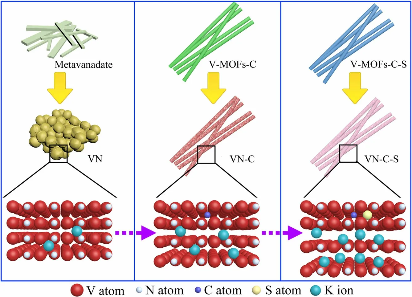
Scheme 1. Schematic diagram of prepared materials (VN, VN-C, and VN-C-S) showing different ions insertion results in different layer spacings.
After being annealed in ammonia atmosphere, the single crystal vanadium nitride that maintains the one-dimensional morphology of V-MOFs precursor was obtained (Figure S5, Supporting Information).The substantially uniform structure of VN, which maintained the V-MOFs precursor, is prerequisite for ensuring fast electron transport and exposing more active surface area in the electrochemical test, and then enables higher electrochemical performance. And the uniform structure and the consistency of local conditions of VN also provide a prerequisite for studying the energy storage mechanism of the material.
The electrochemical behavior of VN electrodes with different heat treatment conditions was measured in a conventional three-electrode system. It is well known that, in crystallography, as the temperature and the thermal treatment time increases,the number of defects in the crystal structure decreases. This is because the crystal defects move toward to the grain boundaries.In order to prove that the electrochemical properties of VN caused by C, S impurity atoms are increased by intercalating VN crystals, instead of being present at grain boundaries,we designed a series of samples with different temperatures and processing times. On the basis of different heat treatment temperatures,times and atoms inserted,we defined the prepared materials as 800 °C-2 h-VN-C-S, 650 °C-2 h-VN-C-S, 500 °C-2 h-VN-C-S, 650 °C-4 h-VN-C-S, and 650 °C-2 h-VN-C, respectively. From the comparison among the cyclic voltammetry(CV)curves(Figure 1a)of different VN electrodes with the same scan rate(50 mV s−1),it can be seen that the redox peaks were almost in the same potential which were identical with previous works.[11,15,21–24]Generally speaking,these two peaks originate from the redox reaction of vanadium during electrochemical measurement.And it also can be seen from figure that the 650 °C-2 h-VN-C-S sample had the largest integral area,indicating a significantly larger specific capacitance. The results of galvanostatic charge/discharge(GCD)curves in Figure 1b are consistent with those of CV curves.Specifically,at a current density of 1 A g−1, the sample of 650 °C-2 h-VN-C-S had a specific capacitance of 191.67 F g−1,but with the same precursor,the specific capacitance of samples obtained by higher temperature (800 °C-2 h-VN-C-S) or longer treatment time (650 °C-4 h-VN-C-S)was only 62.5 F g−1and 104.2 F g−1. And the sample of 650 °C-2 h-VN-C with the same processing conditions had a specific capacitance of 158.4 F g−1. The 500 °C-2 h-VN-C-S had the worst electrochemical performance with a specific capacitance of only 41.7 F g−1. Due to the excessively low annealing temperature, a large amount of organic matter in the product of 500 °C-2 h-VN-C-S was not completely decomposed (Figure S6, Supporting Information),further leading to a bad electrochemical performance. The different electrochemical performances of various samples can be explained by the Nyquist plots and Bode diagram (Figure 1c,d). It can be seen that,at a lower processing temperature of 500 °C, the relaxation time constant of the electrode (~50 s) was much larger than those of the other samples (~1.4 to ~1.7 s), indicating that it can’t perform conventional capacitive energy storage.This also indicates that the processing temperature of the V-MOFs precursors has a great influence on the electrochemical performance of corresponding VN active materials. That is to say,the highest specific capacitance cannot be obtained at too high/low treatment temperature.
In addition to the processing temperature, we found that different embedded atoms in VN materials also have a great impact on the corresponding electrochemical performance, such as 158.4 F g−1of 650 °C-2 h-VN-C and 191.6 F g−1of 650 °C-2 h-VN-C-S. X-Ray Diffraction(XRD) was used to study the influence of embedded atoms on the interplanar spacing of VN crystal, and the results show that the change in specific capacitance was consistent with the shift angle of different samples(Figures S7 and S8,Supporting Information).According to the Bragg equation 2dsin θ = nλ,the shift to a small angle represents the expansion in the layer spacing. In this work, the expansion of the interplanar spacing can only be caused by the doping of impurity atoms of C and S(Figures S9 and S10,Supporting Information).
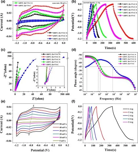
Figure 1. Electrochemical properties of 800 °C-2 h-VN-C-S, 650 °C-2 h-VN-C-S, 500 °C-2 h-VN-C-S,650 °C-4 h-VN-C-S, and 650 °C-2 h-VN-C, in 2 M KOH electrolyte: a) CV curves at scan rate of 50 mV s−1, b) GCD curves at current densities of 1 A g−1, c) Nyquist plots, d) Bode plots; and e) CV curves at various scan rates (5–50 mV s−1), and f) charge/discharge curves at various current densities of 650 °C-2 h-VN-C-S.
As can be seen from the XRD results, larger interplanar spacing brings more excellent electrochemical performance. From the selected area electron diffraction results in Figure 2, we can see more clearly that the (111) interplanar spacing of 650 °C-2 h-VN-C and 650 °C-2 h-VN-C-S are expanded to 0.2443 and 0.2562 respectively, compared with the 0.2361 nm in the standard spectrum (PDF#25-1252).A wider interplanar spacing means a larger exposed active surface area,allowing more metal atoms to participate in the redox reaction during charging and discharging, thereby increasing the charge storage capability of the active material. In order to understand the relationship between them, we intended to establish an OH−traditional theoretical model (Figures S11-S13 and Tables S1-S3, Supporting Information). It can be seen from the optimized results that no matter on what atom OH−was adsorbed at the beginning; it will eventually adhere to V atom uniformly. And from this simulation analysis results, it can be concluded that the most widely accepted hydroxyl adsorption model does not explain the actual experimental results perfectly.
In order to figure out the specific structure evolution of the material during charge and discharge,we performed an ex situ XRD measurement (Figure 3a,b). The relevant potentials for ex situ XRD were selected according to the redox peaks in the CV curves(Figure S14,Supporting Information). It should be noted that before testing, the electrode was cycled for 3 times at a scan rate of 5 mV s−1in advance. In the ex situ XRD patterns, during charging(from 0 V to −1.2 V), the interplanar spacing of (111) gradually decreased, and as the discharge process progresses (from −1.2 V to 0 V), the interplanar spacing gradually became larger.As a result,the change of the interplanar spacing occurred when the material was charged and discharged to different potentials.This change was most likely caused by ion intercalation in the KOH electrolyte. During discharging, K+ions were embedded in the crystal lattice due to charge balance, and a reversible reaction occurred upon charging.This reversible process brings intercalation pseudocapacitance (Figure 3c). Because of this mechanism, which has been reported in the previous works, the structure of VN material will collapse easily.Thus,carbon coating or gel electrolyte coating was applied outside the VN material to make the cycle stability better.[21,25–27]
For understanding the energy storage mechanism of as-prepared VN materials, we carried out in situ Raman experiment (Figure 4a) to explore the structure evolution during charge and discharge. Combined with the results of XRD,we can easily analyze that the energy storage process of vanadium nitride had an important relationship with K+in the solution. During charge process(0 V to −1.2 V), the valence state of vanadium atom rises; the cations diffuse out from the crystal structure.In the blue part of Figure 4a,it is the typical peak position of V4+,which can be seen at the range about−0.2 to −0.7 V.[28]It was mentioned in previous work that the V2+/V3+transition was observed.[29]When the potential window does not reach 0 V,the V2+/V3+transition is not observed.[30]According to our work, we guess that the transition of V3+/V2+may occur near 0 V.The pink part is representative of the typical peak position of V5+, and it can be seen that reversible peak occurs at the end of charge and at the beginning of discharge.[28]When discharging, the cations insert into the crystal,resulting in a decrease in the vanadium valence state.And in the same time, OH−adsorbed on the surface, which simultaneously lead the increase and decrease of the valence state of vanadium (Figure 4b). In this work, the cation is K+. Some previously published works have argued that K+does not play important role in the energy storage process of VN;however,we believe that K+works as a cooperation,[31]and some other work have also proved that OH−reacted with V atom in the host material to output pseudocapacitance.[11]However,here we have proved why VN had the best electrochemical performance in an alkaline environment,[12]which was the cooperation of redox reaction of hydroxide with V atom and insertion and extraction of alkali metal ions in the interplanar spacing, that is the combination of redox pseudocapacitance and intercalation pseudocapacitance. As given in Figure 4c, for the scan rates ranging from 5 mV s−1to 50 mV s−1, the plot had a good linear relationship. The calculated b values for anodic and cathodic peaks were 0.87 and 0.90,respectively,according to the works of Gogotsi and Dunn indicating a fast kinetics mainly contributed by the capacitive process.[32]There is also an obvious peak that cannot be ignored in the green part of Figure 4a. This could be indexed to the peak of V3+, which is due to the irreversible oxidation of the VN by large energy radiation during the Raman test.
The ex situ XRD and in situ Raman measurements have demonstrated the valence changes of V element accompany with the insertion and extraction of K+when scanning to different potentials. In order to study the effect of C and S ions insertion on the geometrical structure of VN,we conducted the first principle calculations(density functional theory, DFT) for VN using the Vienna Ab-initio Simulation Package(VASP). Figure 5 presents the atomic structure evolution of VN after doping C atom, and C and S atoms, respectively. We firstly calculated the C atom insertion equilibrium in VN crystals. As a result, C atom can only insert into the VN lattice in the form of a substituted N atom,thereby displacing the N atoms to the surface. In this state, the total energy of the final system is the lowest, and the system is in the most stable state. Top of the figure points out the lattice constant of VN at normal and inserted C atom showing a lattice expansion to 2.585 ˚A along the c axis as well as the C atom inserting layer, the spacing is reduced to 2.130 ˚A.Bottom of the figure displays the change of the lattice constant of VN when C atom and S atom are simultaneously inserted which shows the lattice is further enlarged along the c axis to 2.588 ˚A and the reduced above mentioned lattice constant also increase to 2.400 ˚A.The N atoms extruded into the crystal lattice are more conducive to the increase in material wettability[33–36]and provide more active sites for the attachment of OH−.
In order to prove that the lattice expansion is meaningful for the diffusion of K+,we calculated the diffusion coefficient(D)of every material based on relevant data(Figure 6,and Equations S1,S2,Supporting Information). The calculated D for 800 °C-2 h-VN-C-S, 650 °C-2 h-VN-C-S, 500 °C-2 h-VN-C-S, 650 °C-4 h-VN-C-S, and 650 °C-2 h-VN-C are 3.54 × 10⁻¹³, 1.81 × 10⁻¹², 2.83 × 10⁻¹⁴, 6.08 × 10⁻¹³and 1.69 × 10⁻¹².Based on the results of above calculation,it is found that 650 °C-2 h-VN-C-S has the highest diffusion coefficient of K+,indicating that the electrochemical kinetics of 650 °C-2 h-VN-C-S is faster than others.
For the sake of further expand the universality of our theory,we have done an extended experiment (Figures S15-S17, Supporting Information). Two common polymers were chosen as impurity atom doping sources. As can be seen from Figure S17, Supporting Information, the electrode material with VN was successfully synthesized.The uniformly reaction of polyacrylic acid (PAA) and VO-3at the chemical molecular level can make C atom easier to dope into host materials.[21]However,polyvinyl pyrrolidone (PVP) can only achieve a uniform mixing at physical level. As a result, which is also consistent with our aforementioned theory, the PAA-based VN can reach a specific capacitance of 329.3 F g−1at 1 A g−1, which is much larger than 160.7 F g−1of PVP-based VN and 45 F g−1of the pure VN. And all the experiments were carried out at a bad high temperature of 800 °C,which is reported as an improper temperature.[11,15]At a current density of 1 A g−1,Figure S16b,Supporting Information shows a typical intercalation pseudocapacitive GCD curve,[37–39]which is consistent with our findings.
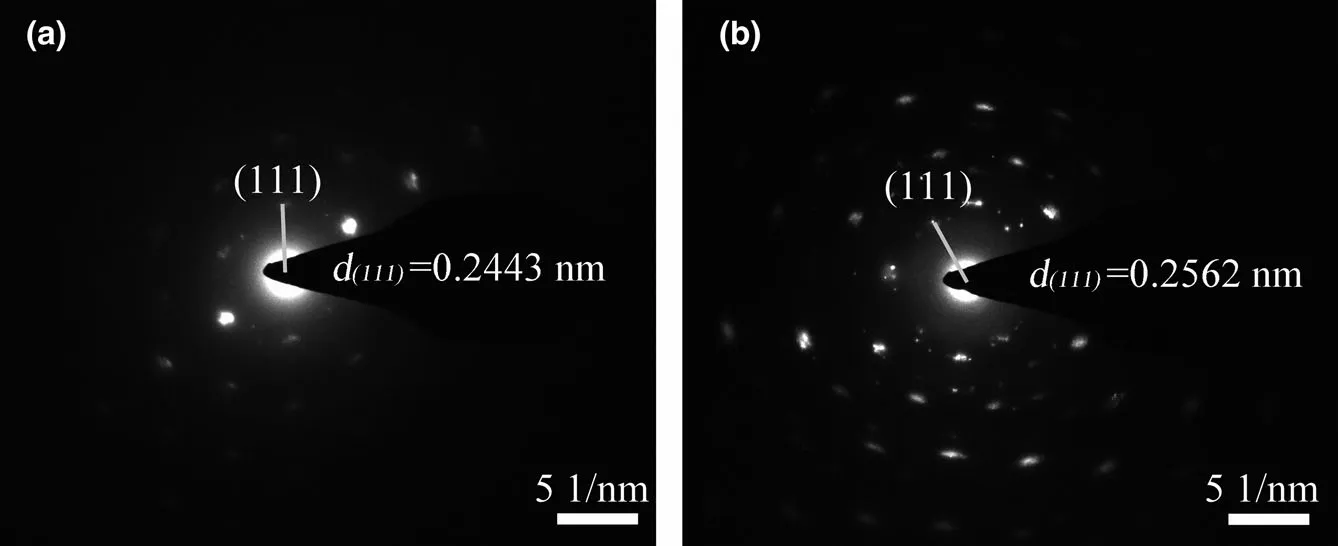
Figure 2. Selected area electron diffraction patterns: a) 650 °C-2 h-VN-C and b) 650 °C-2 h-VN-C-S.
3. Conclusions
In summary, we have successfully obtained VN materials with different interplanar spacing by controlling different anionic V-MOFs precursors, heat treatment conditions and doping atoms.Through comprehensive electrochemical measurements, we found that the specific capacitance of VN materials has a strong connection with the width of interplanar spacing.Through a series of optimizations, the highest specific capacitance of VN materials can be achieved (191.6 F g−1at 1 A g−1). Further,we tested ex situ XRD and in situ Raman to gain a deep understanding of the energy storage mechanism of the material during charge and discharge. According to the obtained results and the theoretical model from DFT simulations,we confirmed the energy storage mechanism for the VN host materials that the insertion and extraction of cations in the crystal lattice and the redox of OH−and V atom together enable charge storage and release, in which the cation actually plays a very important role in this process.Using this theory,we have successfully carried out extended experiments and obtained a high capacitance,329.3 F g−1at 1 A g−1.Based on the recent definition,[40]our work may be of great significance at mechanism research of metal nitride as supercapacitor electrodes and provides useful guidance for developing metal nitride electrodes with higher electrochemical performance.
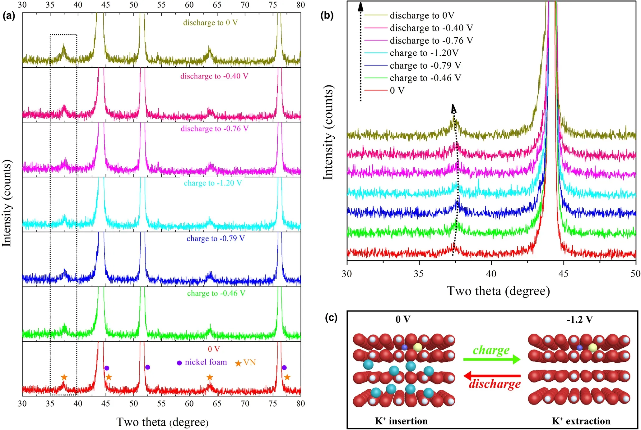
Figure 3. Ex-situ XRD results for 650 °C-2 h-VN-C-S: a) XRD patterns in 30° to 80°, b) enlargement of degree from 30° to 50°, and c) schematic diagram of charge and discharge process.
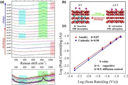
Figure 4. a) In situ Raman spectra of 650 °C-2 h-VN-C-S at different charge and discharge potentials(bottom is raw Raman spectra), b) schematic diagram of pseudocapacitance process and c)determination of the b value using the relationship between the peak current and the scan rate.
4. Experimental Section
Chemicals and Materials: NaVO3, p-phenylenediamine (PPD), 2, 5-diaminobenzenesulfonic acid (BSA),and N, N-dimethylformamide (DMF) were used as received from Sigma-Aldrich. NH4VO3, polyvinyl pyrrolidone (PVP), and polyacrylic acid (PAA) were used as received from Sinopharm.

Figure 5. Atomic structure evolution: initial structure and optimized structure of VN with intercalation of C atom and VN with intercalations of C and S atoms.
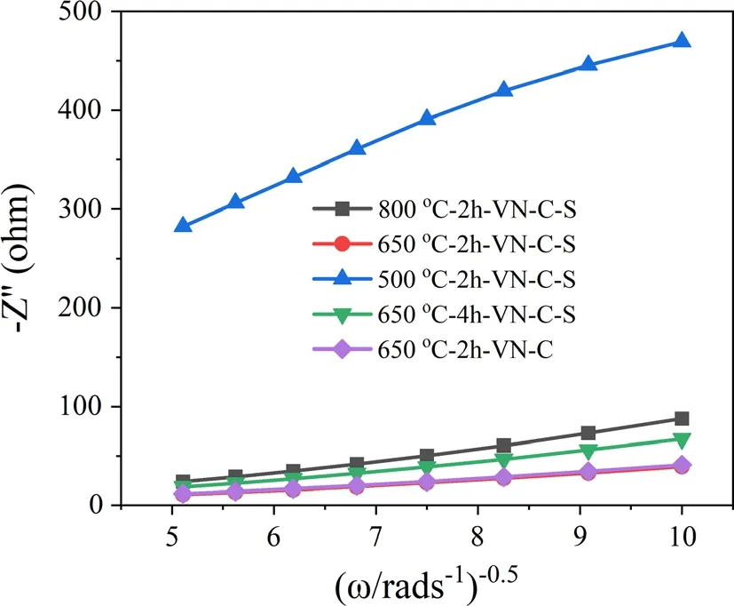
Figure 6. Relationship plots of impedance as a function of the inverse square root of angular frequency in the Warburg region.
Synthesis of V-MOFs: The anionic V-MOFs-C nanowires were synthesized by a hydrothermal method. 0.5 mmol NaVO3and 3.2 mmol PPD (or BSA) were dissolved in the mixed solvents of 5 mL ethanol, 5 mL H2O, and 5 mL DMF. Then the mixture was stirred at room temperature for 4 h to form homogeneously solution,which was then transferred into an autoclave and heat-treated at 160 °C for 4 h. The sample was collected by centrifugation and washed by alcohol and water alternately for five times, and then dried in a vacuum oven at 60 °C for 12 h to obtain V-MOFs.
Fabrication of VN: The V-MOFs as synthesized above were used as precursors and annealed in an NH3/N2(60/40, V/V) atmosphere at 500, 650, and 800 °C for 2 h(the heating rate is 5 °C min−1),respectively.The fabricated samples were marked as VN-C and VN-C-S.
Extended Experiments: 0.1 g NH4VO3was dissolved in 50 mL 1 M HCl, and then dilute ammonia water was added to adjust the PH to 4 to form yellow solution a.1 g of PAA or PVP was mixed with solution a and stirred for 4 h.The mixture was transferred into a 60 °C oven to fabricate VN precursor.All the precursors were heated to 800 °C at a heating rate of 5 °C min−1and annealed in an NH3/N2(60/40,V/V)atmosphere at 800 °C for 2 h.The samples made by the polymers of PAA and PVP were marked as PAA-VN, and PVP-VN; and that did not use polymer was just pure VN.
Material Characterization: The microstructures of the samples were investigated by SEM and TEM.Scanning electron microscopy(SEM)was examined in a Hitachi S-4700 operating at 10 kV, and transmission electron microscopy (TEM)in a Hitachi S-4700 operating at 10 kV and a JEOL 2100F field emission, respectively.The XRD measurements were tested by using a powder XRD(CuKα radiation, PANalytical X’ Pert Pro). X-ray photoelectron spectroscopy (XPS) analysis was performed on a high-resolution Kratos AXIS 165 X-ray photo electron spectrometer using monochromic AlKa radiation.
A Raman instrument of Lab-RAM HR Evolution system (HORIBA,France) connected with a homemade Teflon electrolysis cell, which was used to perform in situ Raman measurement. A Pt SCE was used as the reference electrode and Pt column was used as counter electrode respectively.Here the working electrode included active material and Ni foam substrate.Raman spectra of the sample (one spectrum per 30 s) were captured while a cyclic voltammetry test at a scan rate of 5 mV s−1simultaneously. Before testing, the electrode was cycled for 3 times at a scan rate of 5 mV s−1in advance.
Electrochemical Measurements: Three-electrode cells were assembled to measure the electrochemical properties of the materials. To prepare a working electrode, active material (80 wt.%), carbon black (5 wt.%), acetylene black(5 wt.%), and polytetrafluoroethylene(10 wt.%)were mixed to make a homogeneous black paste. The resulting slurry was spread onto a piece of nickel foam,which served as a current collector. The nickel foam was heated at 60 °C for 10 h in vacuum. Each electrode contained 4 mg of electro-active material and had a geometric surface area of about 1 cm2.
The electrochemical measurements of cyclic voltammetry (CV), galvanostatic charge and discharge (GCD) and electrochemical impedance spectroscopy (EIS)were conducted using a CHI 660D electrochemical workstation(CHI Instruments,China)with a three-electrode cell configuration in 2 M KOH solution.A platinum gauze electrode served as the counter electrode,and a saturated calomel electrode served as the reference electrode.CV and GCD data were collected in the range of−1.2 V to 0 V versus SCE.The cycling tests were performed on an LAND system(CTA2001A, China). The specific capacitance (C) was calculated by the following equation:

where i is the discharge current (A), t is the discharge time (s),m is the mass of active material(g),and V is the potential window(V).
Acknowledgements
This work was partly supported by the National Natural Science Foundation of China (51763014 and 52073133), Joint fund between Shenyang National Laboratory for Materials Science and State Key Laboratory of Advanced Processing and Recycling of Nonferrous Metals(18LHPY002),and the Program for Hongliu Distinguished Young Scholars in Lanzhou University of Technology.
Conflict of Interest
The authors declare no conflict of interest.
Supporting Information
Supporting Informationis available from the Wiley Online Library or from the author.
Keywords
electrode materials, energy storage mechanism, supercapacitors, vanadium nitride, V-MOFs
Received: November 30, 2020
Revised: February 24, 2021
Published online: February 27, 2021
[1] M. Z. Jacobson, Energy Environ. Sci. 2009, 2, 148.
[2] C. Chellaswamy, R. Ramesh, Renew. Sustain. Energy Rev. 2017, 76, 824.
[3] D. Larcher, J.-M. Tarascon, Nat. Chem. 2015, 7, 19.
[4] A. S. Arico, P. Bruce, B. Scrosati, J.-M. Tarascon, W. Van Schalkwijk, Nat.Mater. 2005, 4, 366.
[5] Z. Abdmouleh, A. Gastli, L. Ben-Brahim, M. Haouari, N. A. Al-Emadi,Renewable Energy 2017, 113, 266.
[6] D. P. Dubal, Y. P. Wu, R. Holze, ChemTexts 2016, 2, 13.
[7] A. Gonz´alez, E. Goikolea, J. A. Barrena, R. Mysyk, Renew. Sustain. Energy Rev. 2016, 58, 1189.
[8] P. Simon, Y. Gogotsi, Nat. Mater. 2008, 7, 845.
[9] Y. Zhong, X. Xia, F. Shi, J. Zhan, J. Tu, H. J. Fan, Adv. Sci. 2016, 3,1500286.
[10] B. Gao, X. Li, K. Ding, C. Huang, Q. Li, P. K. Chu, K. Huo, J. Mater.Chem. A 2019, 7, 14.
[11] D. Choi, G. E. Blomgren, P. N. Kumta, Adv. Mater. 2006, 18, 1178.
[12] A. M. Glushenkov, D. Hulicova-Jurcakova, D. Llewellyn, G. Q. Lu, Y.Chen, Chem. Mater. 2010, 22, 914.
[13] A. Morel, Y. Borjon-Piron, R. L. Porto, T. Brousse, D. B´elanger, J. Electrochem. Soc. 2016, 163, A1077.
[14] O. Bondarchuk, A. Morel, D. B´elanger, E. Goikolea, T. Brousse, R. Mysyk,J. Power Sources 2016, 324, 439.
[15] D. Choi, P. N. Kumta, Electrochem. Solid-State Lett. 2005, 8, A418.
[16] P. J. Hanumantha, M. K. Datta, K. S. Kadakia, D. H. Hong, S. J. Chung,M. C. Tam, J. A. Poston, A. Manivannan, P. N. Kumta, J. Electrochem.Soc. 2013, 160, A2195.
[17] F. Cheng, C. He, D. Shu, H. Chen, J. Zhang, S. Tang, D. E. Finlow, Mater.Chem. Phys. 2011, 131, 268.
[18] J. Theerthagiri, G. Durai, K. Karuppasamy, P. Arunachalam, V. Elakkiya,P. Kuppusami, T. Maiyalagan, H.-S. Kim, J. Ind. Eng. Chem. 2018, 67, 12.
[19] P. J. Hanumantha, M. K. Datta, K. Kadakia, C. Okoli, P. Patel, P. N.Kumta, Electrochim. Acta 2016, 207, 37.
[20] Y. Yan, B. Li, W. Guo, H. Pang, H. Xue, J. Power Sources 2016, 329, 148.
[21] Y. Liu, L. Liu, L. Kong, L. Kang, F. Ran, Electrochim. Acta 2016, 211, 469.
[22] Y. Yang, K. Shen, Y. Liu, Y. Tan, X. Zhao, J. Wu, X. Niu, F. Ran, Nano-Micro Lett. 2017, 9, 6.
[23] Y. Wu, Y. Yang, X. Zhao, Y. Tan, Y. Liu, Z. Wang, F. Ran, Nano-Micro Lett. 2018, 10, 63.
[24] H. H. Liu, H. L. Zhang, H. B. Xu, T. P. Lou, Z. T. Sui, Y. Zhang, Nanoscale 2018, 10, 5246.
[25] X. Lu, M. Yu, T. Zhai, G. Wang, S. Xie, T. Liu, C. Liang, Y. Tong, Y. Li,Nano Lett. 2013, 13, 2628.
[26] Y. Liu, L. Liu, Y. Tan, L. Niu, L. Kong, L. Kang, F. Ran, Electrochim. Acta 2018, 262, 66.
[27] Y. Wu, F. Ran, J. Power Sources 2017, 344, 1.
[28] X. Wang, Y. Fei, Y. Xiong, Y. Nie, K. Feng, Chin. J. Light Scattering 2002,13, 1600763.
[29] A. Djire, P. Pande, A. Deb, B. Jason, O. S. Ajenifujah, L. He, A. E.Sleigtholme, P. G. Rasmussen, L. T. Thompson, Nano Energy 2019, 60,72.
[30] K. Robert, D. Sti´evenard, D. Deresmes, C. Douard, A. Iadecola, D. Troadec, P. Simon, N. Nuns, M. Maya, M. Huv´e, P. Roussel, T. Brousse, C.Lethien, Energy Environ. Sci. 2020, 13, 949.
[31] P.Pande,P.G.Rasmussen,L.T.Thompson,J.Power Sources 2012,207,235.
[32] P. Simon, Y. Gogotsi, B. Dunn, Science 2014, 343, 1210.
[33] Z. Y. Wu, H. W. Liang, L. F. Chen, B. C. Hu, S. H. Yu, Acc. Chem. Res.2016, 49, 96.
[34] X. Liu, T. Sun, J. Hu, S. Wang, J. Mater. Chem. A 2016, 4, 3584.
[35] C. Liu, C. Li, K. Ahmed, Z. Mutlu, I. Lee, F. Zaera, C. S. Ozkan, M.Ozkan, Small 2018, 14, e1702444.
[36] C. O. Ania, V. Khomenko, E. Raymundo-Pi˜nero, J. B. Parra, F. B´eguin,Adv. Func. Mater. 2007, 17, 1828.
[37] M. R. Lukatskaya, B. Dunn, Y. Gogotsi, Nat. Commun. 2016, 7, 12647.
[38] Y. Gogotsi, R. M. Penner, ACS Nano 2018, 12, 2081.
[39] Y. Liu, Q. H. Wu, L. Y. Liu, M. Pantrangi, L. Kang, F. Ran, J. Mater. Chem.A 2020, 8, 8218.
[40] Y. Q. Jiang, J. P. Liu, Energy Environ. Mater. 2019, 2, 30.
杂志排行
Energy & Environmental Materials的其它文章
- Progress of Pb-Sn Mixed Perovskites for Photovoltaics:A Review
- Development Strategies in Transition Metal Borides for Electrochemical Water Splitting
- Polymer-/Ceramic-based Dielectric Composites for Energy Storage and Conversion
- Controllable Construction of Bifunctional CoxP@N,P-Doped Carbon Electrocatalysts for Rechargeable Zinc–Air Batteries
- Unveiling the Underlying Mechanism of Transition Metal Atoms Anchored Square Tetracyanoquinodimethane Monolayers as Electrocatalysts for N2 Fixation
- Rational Design of High-Performance Bilayer Solar Evaporator by Using Waste Polyester-Derived Porous Carbon-Coated Wood
