Granular structure of chromium coatings prepared by arc ion plating for accident-tolerant fuel cladding
2022-06-17-,-,--,,,-,,-,-
-, -, --, , , -, , -, -
(1.Science and Technology on Reactor Fuel and Materials Laboratory, Nuclear Power Institute of China, Chengdu 610200, China;2.Key Laboratory of Radiation Physics and Technology, Ministry of Education,Institute of Nuclear Science and Technology, Sichuan University, Chengdu 610065, China)
Abstract: This paper depicts a detailed configuration of the arc-ion-plated Cr coatings by a multiscale characterization from about tens of microns to several angstroms. Characterized by XRD, SEM, FIB, TEM and HRTEM, the coatings show a multiple configuration including the micron-sized particles on the surface, the micron or submicron-sized droplets pinned by defect bands around, the columnar grains with stacked faults as boundaries, the ambiguous crystallites differentiated with edge and screw dislocations, the atomic distortions on the ends of these dislocations, and some disordered regions. These structures are found to affect the crystal constant, surface coarsening, and FIB-sputtered cracks by changing the coating crystallinity. In addition, the types of stacking faults and dislocations are confirmed by analyzing the HRTEM images. And finally, the effects of depositing parameters on the granular structure are also discussed.
Keywords: Coating; Chromium; Arc ion plating; Grain; Microstructure
1 Introduction
Demand of Cr coatings are motivated as a short-term solution for protecting Zr claddings from a possible loss-of-coolant accident (LOCA) because of their resistance to oxidation and irradiation, and compatibility with current reactor fuel technologies[1-6]. To fit for violent environments and tubular claddings in nuclear reactors, common viewpoints on these coatings are thick enough to tens microns and economical in a fast deposition[2], which is often difficultly satisfied by some refining-deposition technologies like the magnetron filtering[7], magnetron sputtering[8-10]and ion-beam sputtering[11]for an engineering use. And by searching, deposition of such Cr coatings has been easily performed by the arc ion plating[12], which attracted attentions of researchers in accident-tolerant fuel (ATF) claddings[13-20]. But in spite of being a single-element coating, the fast deposition with many liquid droplets, atomic groups and charged ions in the arc-ion-plating process inevitably coarsens its structural configurations including big particles, preferred phases, grains, defects, boundaries and even surface morphology[16], which is different with refined coatings featured with columnar grains.
Besides the arc-ion plated Cr coatings,similarly coarsened granular structures prepared by plasma treating[21], 3D laser coating[22, 23], cold spraying[24-27]and even electroplating[28-30]are also found, at least on their surfaces. Such a multi-scale configuration including micron-sized particles on the surface, submicron-sized grains, nano-sized crystallites and atomic-scale disordering should be considered in applications, although some effects of single-type structures have been confirmed. For example, inter-grains boundaries might deplete irradiation-induced defects[31]and impede the motion of dislocations, grainy morphologies might provide loose boundaries for the penetrations of heat and diffusing atoms under steam oxidation[2, 33], and in-grain atoms also were possibly recrystallized by displacing atoms in irradiation[20]. Indeed, a complex configuration means unexpected changes in the coating property, especially on an ATF cladding in a radioactive environment.
Past separated studies referred to different scales of the Cr coating structures. Micron-sized protrusions and droplet particles were found on arc-ion plated Crcoatings[20]. Micron-scale pores and particles in the arc-ion plated Cr coatings were reduced by a laser melting technology for a high density[18]. In sub-micron scale, the grain diameter, orientation, texture, and dislocations were also studied for deposited Cr coatings at several arc currents[17]. In atomic scale, the 1/2<111> dislocation in the Cr coating was believed to be important for the plasticity of BCC metals[33, 34], and interface structures were studied on ZrCr2laves phases[35]. Obviously, these reported structures are isolated from a collective form for the Cr coatings, which needs a multi-scale characterization.
In this paper, the multi-scale observation was performed from micron-sized particles to atomic scale to present a clear granular configuration of the arc-ion-plated coatings.
2 Experimental
The Cr coatings were deposited on Zr alloy substrates in a vacuum chamber by the arc ion plating technology, also called multi-arc ion plating[36]or vacuum cathodic arc deposition. The Cr target and incoming Ar gas were 99.9% and 99.99% pure, respectively. The target size was 10 cm large enough for an engineering production, where a prediction of large-droplet deposition was existent due to the large target with a possible inhomogeneity of the arc current. In processing, the substrate temperature, pressure, arc current and negative bias voltage were orthogonally changed in a wide range during the depositing process, as shown in Tab. 1. In spite of non-single change for the parameter setting, the deposited coatings were also ordered by the surface crystallinity intensified by XRD-measured (110) peaks, more accurately, called as the (110)-oriented crystallinity. So, these nine samples were renumbered after the experiments for a structural analysis.
To analyze morphologies on the surfaces and in the coatings, the X-ray diffraction (XRD, EMPYREAN,PANalytical), the scanning electron microscope (JEOL, JSM-7500F), the focused ion beam (FIB, FEI Helios NanoLab 600i), the transmission electron microscope (TEM, FEI Talos F200X) and high-resolution TEM (HRTEM) were used to characterize the Cr coatings. Specially, in the XRD measurements, the used Cu Kα1 and Kα2 X rays were 0.154 059 8 and 0.154 442 6 nm in wave length and the crystal constants of the coating was calculated according to the Kα1 wavelength and peak positions (2theta) according to the Bragg’s law. In the SEM characterization, EDS was also performed but its results made no difference for all deposited coatings. In the FIB processing, a Pt film was firstly deposited for protection, then the Ga ion beams with the Lift-Out mode were used to sputter the coatings, and finally slices with a size of about 100 nm thick were dug out for TEM observation. And for HRTEM, part of each slice was thinned to about 60 nm thick and fast Fourier transformation (FFT) of the selected regions in the HRTEM images was performed with the TEM-included software.
3 Results
>Fig. 1a~1c show the XRD peaks and their positions of the samples which are considered as crystallinity for the following shows and discussion. To get a clear view of peak shifts, the XRD (110) and (200) peaks are shown separately in Fig. 1a and 1b, and thus can be used to calculate the crystal constant shown in Fig. 1c. So, a relation of the crystallinity and crystal constant is available, where the crystal constant tends to be decreased with increasing the (110) peak intensity. This result is reasonable for a smaller atomic spacing in an ordered array of Cr atoms than in a disordered one.


Fig.1 XRD (110) (a) and (200) (b) peaks for the Cr coatings, and the calculated crystal constants (c) by using these peaks
As motivated by the relation of the crystal constant and intensity in Fig. 1c, the calculated crystal constant of the samples can be plotted as a function of the droplet diameter, which is shown in Fig. 2c. Although the curve is fluctuated, the crystal constant tends to be increased with increasing the droplet diameter.
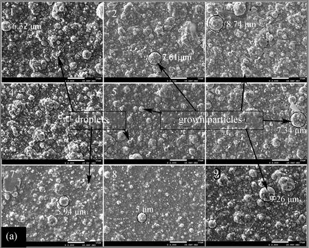

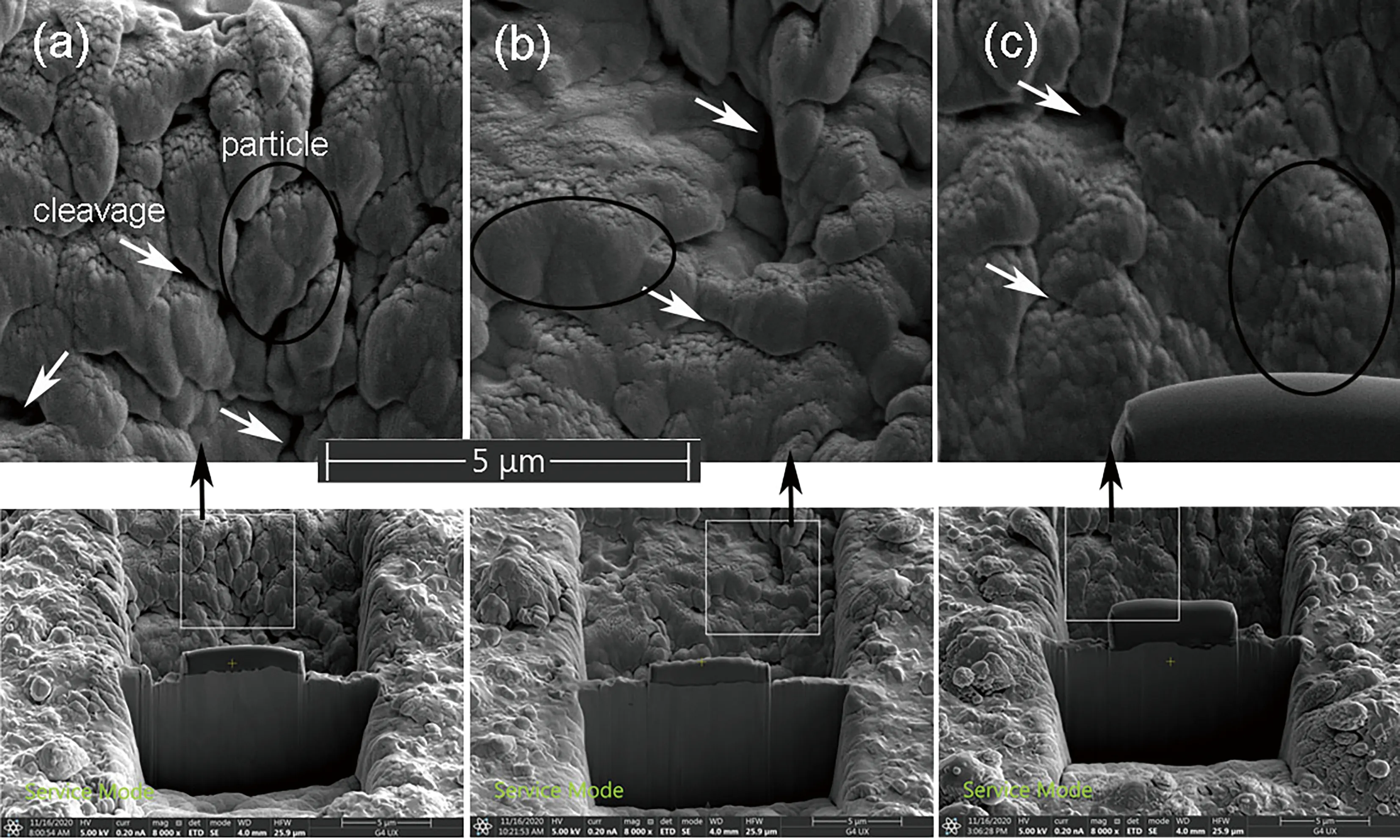
Fig.3 FIB images of the coatings 4# (a), 7# (b) and 9# (c), with circles for particles and white arrows for sputtered cleavages or pores
To make the grain boundaries clear, Fig. 5a and 5b show HRTEM images for the samples 4# and 7#, respectively. Fig. 5a1~5a3 are binned FFT images of the selected regions in Fig. 5a, and Fig. 5b1~5b3 are FFT for Fig. 5b. It can be seen that the widths of the boundaries are more than 20 nm for the coating 4# and lower than 10 nm for the coating 7#. And in Fig. 5a, the grain boundary (GB) is located between two gains: one is the observed (100) plane with diffracting (110) and (100) families shown in the FFT images of Fig. 5a1, and the other one is two different planes with two sets of diffraction spots in the FFT images of Fig. 5a3. Seen from the atomic images of Fig. 5a3, the same set of diffraction spots with the long arrows as the one of Fig. 5a1 is obviously attributed to the atomic array close to the GB, and the other set is with the unknown families of the 0.234 and 0.240 nm spacing planes and the (200) family, which is the real spots of the nether grain marked with the short arrows in the FFT image of Fig. 5a3. This lattice difference with BCC means a misfit of the atomic array driven by the GB. As shown in Fig. 5a2, the GB is composed of a list of stacking faults and the stacked spacing is 0.608 nm (see the FFT image of Fig. 5a2),i.e., three times of the (110) planar spacing of 0.203 nm. Similarly, the GB in Fig. 5b is also composed of stacking faults despite a small width and the stacking spacing is 0.685 nm which is a little larger than that in Fig. 5a2 due to the angle difference to the (110) families or in the observing direction. These stacking faults may be along (112) plane families, which has been studied as a generalized fault in BCC boundaries[37, 38].
Fig. 6 is the HRTEM image of sample 9# and binned FFTs of the selected region for confirming dislocations in the Cr coating. In overview, the black spots may be attributed to the concentration of compressive stress, and disordering of these crystals and misfitting in BCC lattices are found to be interlocked. To make defects clear, some atoms around several misfits are emphasized by circles in Fig. 6. Thus, observed on the (001) plane in Fig. 6a and 6b the 1/2 (100) edge and 1/2 (100) screw dislocations can be found. And observed on the (111) plane in Fig. 6c and 6d, disordered regions and dislocations are shown, where the edge dislocation in the illustrated curve in Fig. 6c is 1/2 (111). Although not clearly observed, the 1/2 (111) screw dislocation might be positioned around the disordered parts or black spots. Of course, the HRTEM images show that the multiple dislocations prevail throughout the coating, since a single dislocation is not stable in a perfect crystal due to climbing of metal atoms. And finally, in angstrom size, the atom displacement to its lattice site is often at the sites of the dislocation ends.
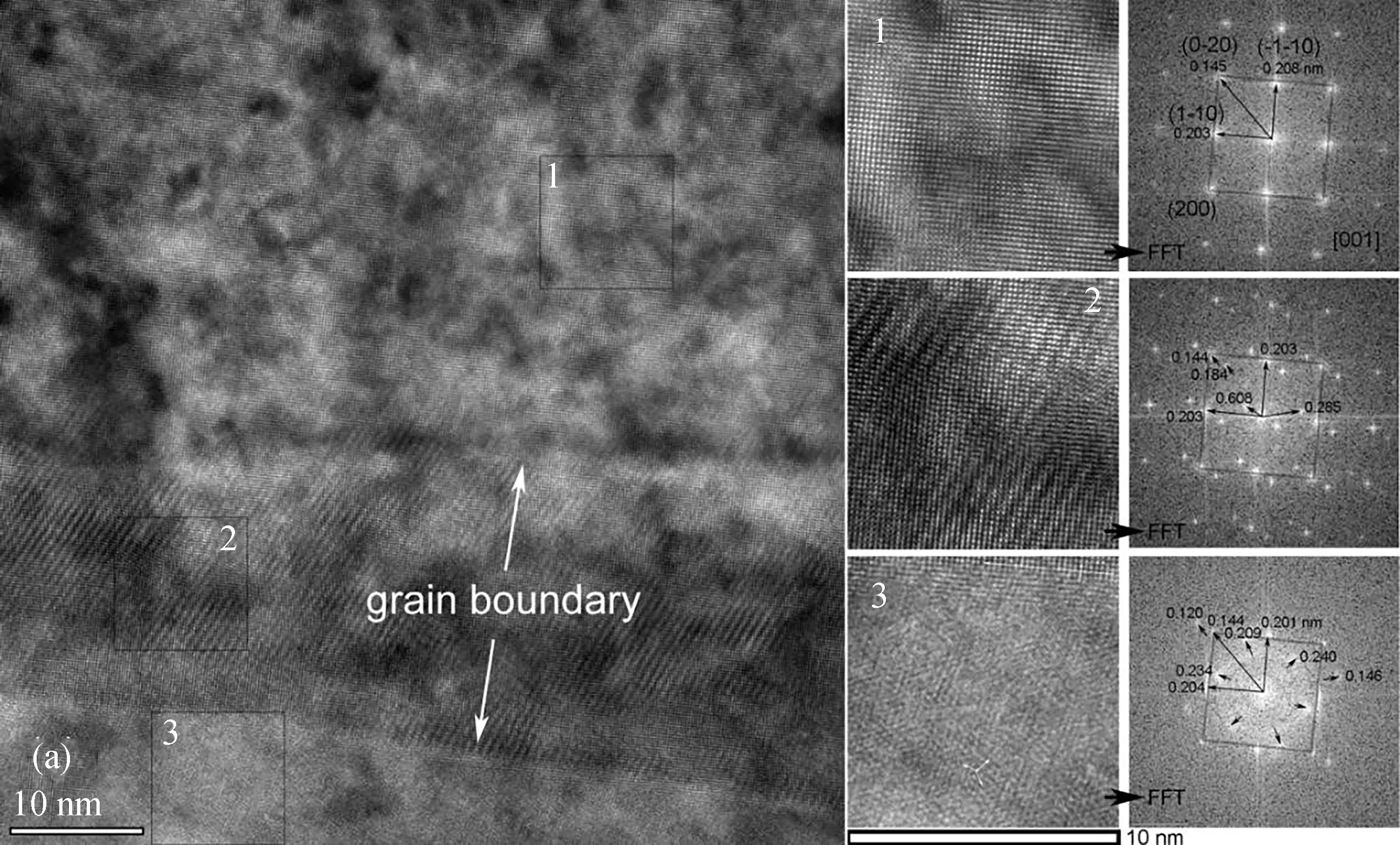
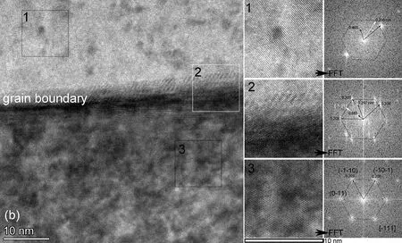
Fig.5 HRTEM images of grain boundaries and their grains, and binned FFT images of selected regions for the samples 4# (a) and 7# (b)

Fig.6 Enlarged HRTEM images of crystal misfits for edge, screw dislocations, and disordering, on (001) planes (a and b) and on (111) planes (c and d)
4 Discussion
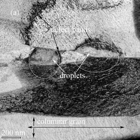
The results of Fig. 2 and Fig. 3 show that the micron-sized configuration is the particle-like protrusions and droplets, which were easily observed on the surface and even cleaved to be observable on the FIB images in the coatings. And these particles or droplets are surrounded by the defect bands shown in Fig. 4. In general, with increasing the coating crystallinity, the particles-like situation and the droplet size are weakened in general, at least the defect bands may be decreased in size or number as shown in Fig. 4.
As depicted in Fig. 4 and Fig. 5, the submicron-sized configuration is the columnar grains and their boundaries, which is normal for all the physical vapor depositions. But the coexistence of droplets and columnar grains should be special for the arc ion plating. Exactly, the columnar grains pin the droplets with the defect bands around, since their length and width are enough large to match the coating thickness of 20~30 μm. And their boundaries with tens nanometers wide are composed of stacked faults due to the misfits of two adjacent grains.
Innano-sized configuration, unlike the differentiable in-grain crystallite demarcated with amorphous parts or perceptible defects in compounds or alloys[39], the called crystallites in the Cr coatings are only to show the oriented atomic arrays divided by dislocations in the observed plane, since they might be not evidently differentiated in a three-dimensional network of dislocations. And from the HRTEM images the crystallites are not easily confirmed due to the long-range order of metal atoms. But the edge and screw dislocations in Fig. 6 make the range of a well-arranged crystallite limited in about 5 nm. Also, the nano-sized disordered regions and dislocations are inter-locked, which indeed makes the crystallites slightly deflected or brightness different with each other, which is the difference of the Cr coating with compounds or alloys. Besides, in such a 3-dimensional dislocation-concentrated network, counting of the dislocations need more studies to give a reliable dependency on experimental parameters. Unfortunately, information for these fine structures in measurements might be covered by that of other bigger defects, like boundaries, defect bands, even though the collective information for all defects was measurable by XRD.
Finally, combined with Tab. 1(the preparing parameters of the coatings arranged according to the (110) crystallinity of XRD), the surface morphology in Fig. 2 is smoothened with decreasing the arc current, but, for the large current of 150 A, large values of the temperature, pressure and bias voltage are needed to obtain a high (110) crystallinity for the coating 9# in Fig. 1. This means the importance of the arc current other than other parameters. For instance, increases of the bias voltage regarded as effective ways to change the preferred orientation[8]is not crystallinity dominant in the coatings, with taking the (200) peaks in Fig. 1b as a reference. However,increasing the deposition temperature was found to seldom change coating properties[40]and also to be equivalent to an increase of the bias voltage via increasing ion bombardment[41, 42]. The result also shows a difference with the reported data[19], especially on the dependence of the preferred orientation on the temperature and arc current. The special of the ATF-demanded Cr coatings is big droplets from the fast deposition in the arc ion plating. Although a physical image of columnar grains is an obvious view, the pinned droplets dependent on the arc current may take a main function in the formation of defect bands.
5 Conclusions
(1) Particles, droplets, grains, crystallites and defects were clearly observed from about ten microns to several angstroms in the Cr coatings prepared by the arc ion plating, which indeed show a multiple configuration. And defect bands around particles or droplets, stacked faults between columnar grains, dislocations anddisordering in crystallites are confirmed.
(2) With increasing the (110)-oriented crystallinity in the XRD measurements, the coating tends to be in reduction of particles and droplets, growth of columnar grains and little change of in-grain dislocations. And the granular structure is believed to be influenced dominantly by the arc current and also collectively by other parameters.
(3) Localized atomic disordering, (112) stacking faults, 1/2 (100) edge, 1/2 (111) edge and 1/2 (100) screw dislocations may prevail in the arc-ion-plated Cr coatings.
The results indicate that the reduction of droplets in the arc-ion-plating deposition is important to get a high-quality Cr coating and the effect of defect bands and grain boundaries in irradiation should be re-apprised for its use on ATF claddings.
