High-efficiency Blue Phosphorescent OLEDs Based on Mixed-host Structure by Solution-processed Method
2022-05-23WANGZheWURuixiaFENGYangLIUHuaZHOULiang
WANG Zhe, WU Rui-xia, FENG Yang, LIU Hua, ZHOU Liang*
(1. State Key Laboratory of Rare Earth Resource Utilization, Changchun Institute of Applied Chemistry, Chinese Academy of Sciences, Changchun 130022, China;2. Center for Advanced Optoelectronic Functional Materials Research, and Key Laboratory of UV Light-emitting Materials and Technology of Ministry of Education, Northeast Normal University, Changchun 130024, China)*Corresponding Authors, E-mail: liuh146@nenu.edu.cn; zhoul@ciac.ac.cn
Abstract: Blue phosphorescent organic light-emitting diodes(PHOLEDs) which utilized TcTa and CzSi as the mixed-host were fabricated to improve the efficiency by solution-processed method. Additionally, three electron transport materials Tm3PyP26PyB, TmPyPB and TPBi were employed to further enhance the efficiency of devices. The efficiency was improved by optimizing the ratio of host materials and the selection of electron transport material. Finally, the optimal device with the doping ratio TcTa∶CzSi of 6∶1 and 70 nm TPBi layer exhibited the maximum brightness(Bmax), current efficiency(CEmax), power efficiency(PEmax) and external quantum efficiency(EQEmax) of 6 662 cd·m-2, 39.40 cd·A-1, 23.33 lm·W-1 and 19.7%, respectively. Moreover, outstanding current efficiency and external quantum efficiency as high as 33.43 cd·A-1 and 16.7%, respectively, were obtained, even at the practical brightness of 1 000 cd·m-2.
Key words: organic light-emitting diodes; high efficiency; solution-processed; mixed-host structure; blue emission
1 Introduction
Organic light-emitting diodes(OLEDs) are the most promising new display and lighting technology owing to their unique advantages of thinness, quick response, high contrast ratio, energy efficiency and being used in flexible electrical appliances[1-3]. It is widely used in smart phone displays, TV screens and computer monitors,etc. However, due to the limitation in vacuum thermal evaporation technology, OLEDs have encountered great difficulties in meeting the requirements of low-cost and high-resolution for large-size OLED devices. Therefore, solution-processed OLEDs which have a variety of advantages, such as low fabrication cost, easily scalable manufacturing and the potential in producing large-area devices, have attracted great attention[4]. Conventional OLEDs are typically composed of four or more multiple layers of different materials, thus achieving notable increase in efficiency and lifetime. However, it is more difficult to construct so many layers in the case of solution-processed method, because depositing one layer would dissolve its next layer[5]. Up to now, the blue device still has the issue of low efficiency. In this case, improving the efficiency of blue devices fabricated by solution-processed method becomes more challenging[6].
In recent years, significant improvement has been achieved regarding to solution-processed OLEDs[7-9]. The mixed-host structure has been proposed and its superior advantages in reducing layer structure and improving device performance has been demonstrated. The mixed-host structure used in solution-processed OLEDs is more beneficial for balance the carriers and broaden the recombination zone than the single-host. Chenetal. fabricated blue OLEDs using electron-type host material 2, 7-bis(diphenylphosphoyl-9, 9′-spinodimer[fluorene](SPPO13) and hole-type host material 4,4′,4″-tris(9-carbazolyl)triphenylamine(TcTa)[10]. The luminous efficiency and efficiency roll-off of devices were significantly enhanced and improved by exploiting mixed-host structure than single-host structure. Finally, the optimal device with the doping ratio SPPO13∶TcTa of 6∶3 demonstrated the CEmaxof 34.3 cd·A-1and EQEmaxof 15.2%. Kumaretal.selected poly(N-vinylcarbazole)(PVK) and 1,3-bis(N-carbazolyl)benzene(mCP) as host materials for efficient red-orange TADF solution-processed OLEDs. The efficiency, lifetime and stability of devices were notable improved by reducing the self-aggregation of TADF emitters. Finally, the optimal device realized the EQEmaxof 9.75%, CEmaxof 19.36 cd·A-1and PEmaxof 12.17 lm·W-1by using the mixed-host structure[11]. In addition, the transmission characteristics of the host materials and the well-matched energy levels between the functional layers are also important factors for the optoelectronic performance of devices.
In this paper, a series of blue phosphorescent devices which utilized iridium(Ⅲ)[bis(4,6-difuorophenyl)pyridinato-N,C2’]picolinate(FIrpic) as emitter were fabricated to enhance device performances by constructing mixed-host structure consist of TcTa and 9-(4-tert-Butylphenyl)-3,6-bis(triphenylsilyl)-9H-carbazole(CzSi). In addition, the selection of electron transport material was optimized to further improve the efficiency of blue phosphorescent devices. The optimal device displayed theBmax, EQEmax, CEmaxand PEmaxup to 6 662 cd·m-2, 19.7%, 39.40 cd·A-1and 23.33 lm·W-1, respectively. Even at the practical brightness of 1 000 cd·m-2, current efficiency and external quantum efficiency reach up to 33.43 cd·A-1and 16.7%, respectively, can still be maintained. The high efficiency blue OLEDs with mixed-host structure have been achieved by selecting appropriate host and electron transport material.
2 Experiments
All organic materials and solvents were obtained commercially and used as received without further purification. Indium-tin-oxide(ITO) coated glass with a sheet resistance of 10 Ω·□-1was used as the anode. The ITO glass substrates were cleaned with detergent and de-ionized water and finally dried in an oven before preparing the devices. After that, ITO substrates were treated with UV-ozone for 20 min. Poly(3,4-ethylenedioxythiophene)∶poly(styrene sulfonate)(PEDOT∶PSS) was spin-coated on ITO substrates at 3 000 r/min for 60 s and annealed at 120 ℃ for 20 min. Afterward, the samples were moved into the glove box. The luminescent and host materials were dissolved in chlorobenzene solution at 4 mg·mL-1and 10 mg·mL-1, respectively. After the solutions of luminescent material and host materials were prepared in proportion, they were dropped on the ITO substrate. The light-emitting layer(EML) was spin-coated at 3 000 r/min for 30 s and annealed at 70 ℃ for 30 min. And then, electron transport layer(ETL) was deposited with the rate of 0.1 nm·s-1under vacuum(≤ 3.0×10⁻⁵Pa). LiF and Al were deposited in another vacuum chamber(≤ 8.0×10⁻⁵Pa) at 0.01 and 1.0 nm·s-1, respectively. The current density-voltage-brightness(J-V-B) characteristics of devices were measured by using a programmable Keithley source measurement unit(Keithley 2400 and Keithley 2000) with a silicon photodiode. The EL and photoluminescence(PL) spectra were measured by using a calibrated Hitachi F-7000 fluorescence spectrophoto-meter.
3 Results and Discussion
3.1 Optimization of Doping Ratio of Host Materials
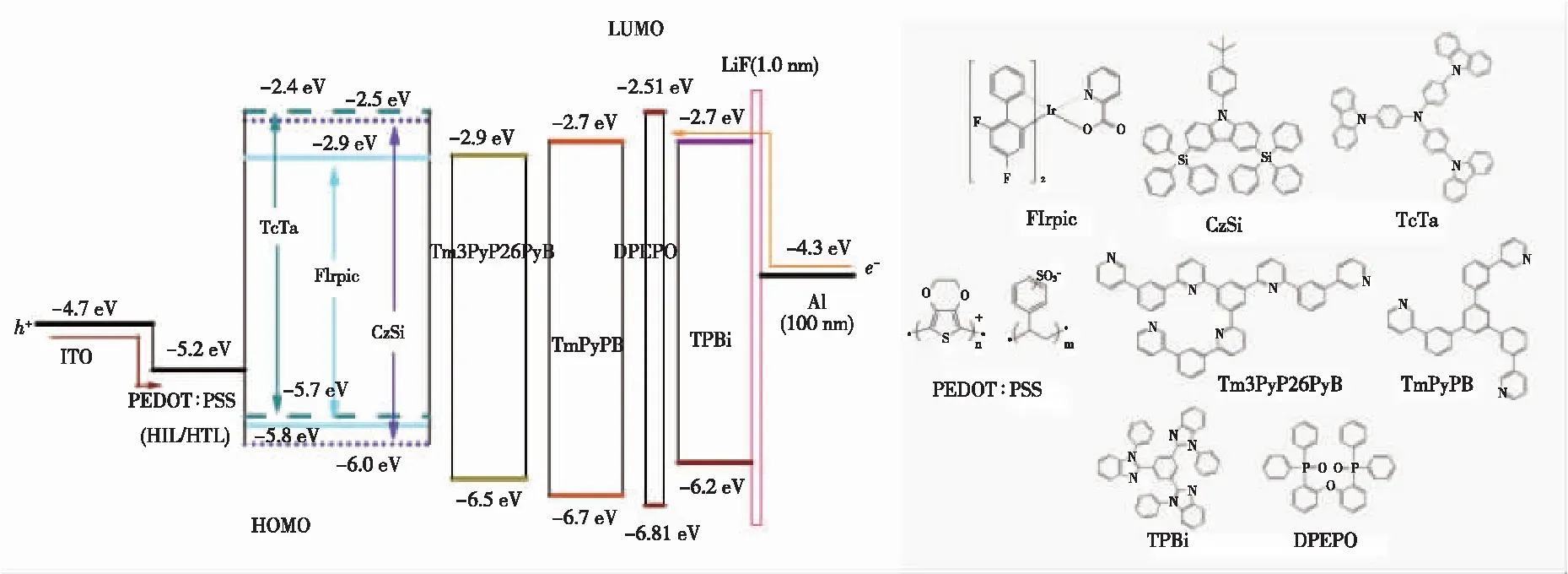
Fig.1 shows the energy level diagrams of devices and molecular structures of materials used in these devices.PEDOT∶PSS was used as hole injection and transport material. FIrpic was selected as the luminescent material since it is one of the most commonly used blue phosphorescent material. The energy level of host materials should be higher than that of FIrpic(ET=2.62 eV) as far as possible to prevent the energy transfer from guest to host[12-13]. In this case, CzSi and TcTa were employed as the host materials. CzSi(ET=3.02 eV) has a high triplet energy level, which enables effective energy transfer from host to guest and reduces energy loss during the transfer process. Simultaneously, TcTa has excellent hole transport capability, which can compensate the deficiency of solution-processed devices in hole transport. Therefore, the designed TcTa and CzSi mixed-host structure can effectively balance the charge within the EML. In this part of experiment, 1,3,5-tris(6-(3-(pyridin-3-yl)phenyl)pyridin-2-yl) (Tm3PyP26PyB) was chosen as electron transport material due to its excellent electron transport properties. Moreover, LiF and Al were utilized as electron injection material(EIL) and the cathode, respectively. To determine the optimal doping concentration of FIrpic, a series of devices with structure of ITO/PEDOT∶PSS/FIrpic(x%)∶CzSi/Tm3PyP26PyB(60 nm)/LiF(1 nm)/Al(100 nm) were first fabricated and then measured. The 14% doped EML device exhibited CEmax, PEmax,Bmaxand EQEmaxup to 10.26 cd·A-1, 4.68 lm·W-1, 4 163 cd·m-2and 5.6%, respectively. Subsequently,we introduced TcTa as mixed-host together with CzSi based on the above device architecture to investigate the device performances in mixed-host structure.

Fig.1 Energy levels diagram of the devices used in this work and the molecular structures of FIrpic, CzSi, TcTa, PEDOT∶PSS, Tm3PyP26PyB, TmPyPB, TPBi and DPEPO.
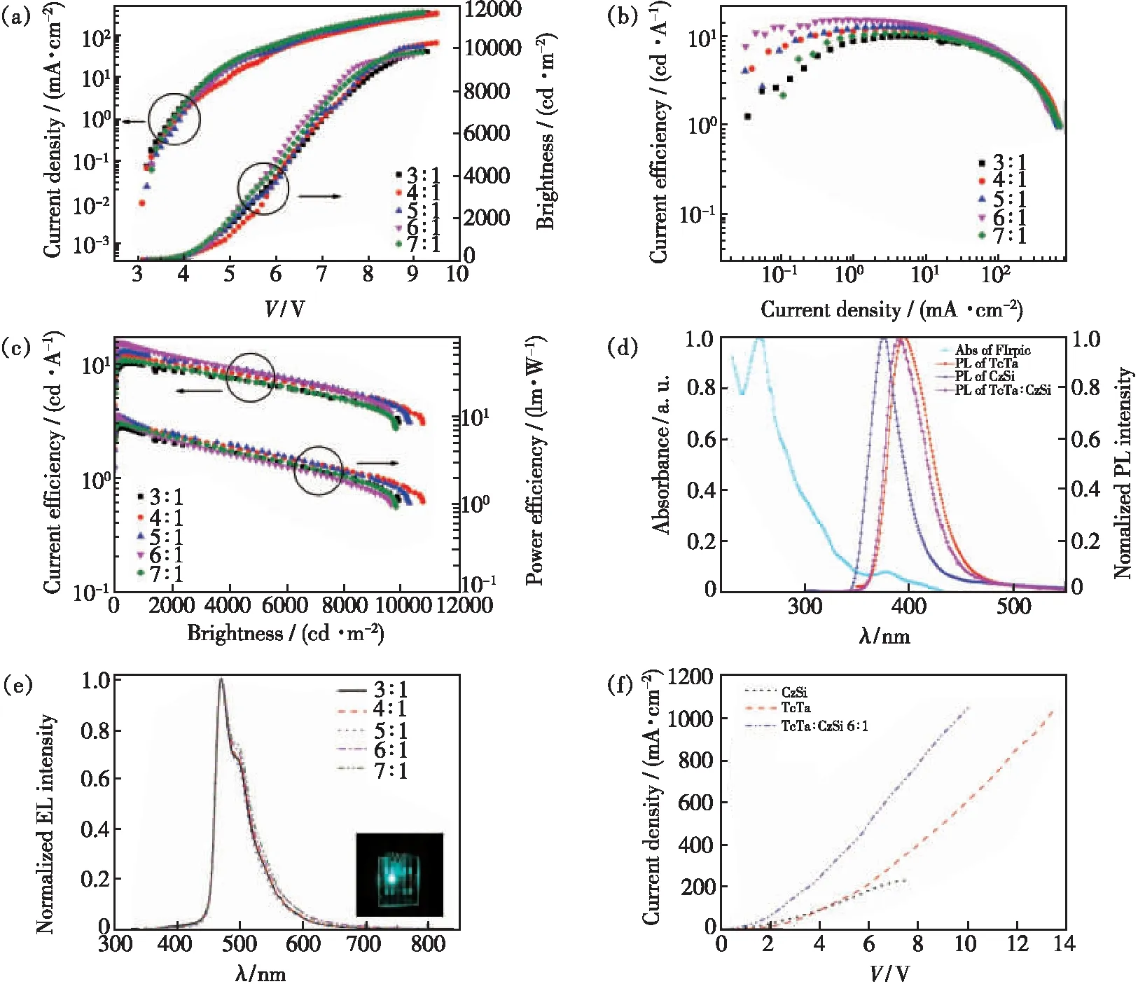
Figs.2(a)-(c) depict current density-voltage-brightness(J-V-B) characteristics, the current efficiency-current density(ηc-J) characteristics and current efficiency-brightness-power efficiency(ηc-B-ηp) characteristics of devices with different doping ratios of TcTa∶CzSi, respectively. With the increase in the proportion of TcTa, the current density and current efficiency of devices gradually increased. Moreover, the efficiency of different doping ratios varied little with brightness. Generally, the devices with PEDOT∶PSS lack holes within EML due to the large energy gap of hole injection and the high electron mobility of Tm3PyP26PyB, which cause the unbalanced carriers’ distribution and the annihilation of excitons. In addition, electrons can transit directly to the guest molecules because of the same lowest unoccupied molecular orbital(LUMO) levels of Tm3PyP26PyB and FIrpic. Obviously, the recombination zone is near the interface between PEDOT∶PSS layer and EML. Fig.2(d) shows the PL spectra and absorption spectra. The peaks of the PL spectra of TcTa, CzSi and TcTa∶CzSi were at around 395, 375, 389 nm, respectively. The TcTa∶CzSi mixed-host exhibited combined emission of TcTa and CzSi. Therefore, the mixed-host could combine the advantages of the two host materials, which had a good overlap with the absorption spectra of FIrpic, and excitons can transfer from host to FIrpic.Therefore, the hole injection and transport capabilities of the devices could be improved and the recombination zone should be broadened by increasing the doping ratio of TcTa. When the doping ratio of TcTa∶CzSi was 6∶1, the device(device A) achieved the CEmax, PEmax,Bmaxand EQEmaxup to 15.23 cd·A-1, 10.32 lm·W-1, 9 639 cd·m-2and 7.6%, respectively(see Tab.1). Consequently, the mixed-host devices exhibit higher performances compared with single-host devices.

Fig.2 (a)Current density-voltage-brightness(J-V-B) characteristics of devices with different doping ratios of TcTa∶CzSi. (b)Current efficiency-current density(ηc-J) characteristics of devices with different doping ratios of TcTa∶CzSi. (c)Current efficiency-brightness-power efficiency(ηc-B-ηp) characteristics of devices with different doping ratios of TcTa∶CzSi. (d)Absorption spectra of FIrpic and PL spectra of TcTa, CzSi and TcTa∶CzSi. (e)Normalized EL spectra of devices with different doping ratios of TcTa∶CzSi operating at 10 mA·cm-2. Inset: Photograph of blue OLED. (f)Current density-voltage characteristics of single-hole devices.

Tab.1 Key properties of devices with different doping ratios of TcTa∶CzSi
a The data for maximum brightness(B), b Maximum current efficiency(ηc), c Maximum external quantum efficiency(EQE), d Maximum power efficiency(ηp), e Current efficiency(ηc) at the certain brightness of 1 000 cd·m-2, f External quantum efficiency(EQE) at the certain brightness of 1 000 cd·m-2, g Commission Internationale de L’Eclairage coordinates(CIE(x,y)) at 10 mA·cm-2.
Meanwhile, the characteristic emission peak and shoulder peak of FIrpic were observed at around 470 nm and 500 nm, respectively, as depicted in Fig.2(e)[14-16]. Furthermore, the curve progression is very similar and there is no obvious shift in the spectra, which illustrates the stability of the devices. The host emission could not be found in the spectra, indicating that the energy transfer was almost complete between host and guest.
To better illustrate the mixed-host structure enhanced the hole transport ability and thus increased the device efficiency, we fabricated a series of single-hole devices with the structure of ITO/PEDOT∶PSS/TcTa/HAT-CN(10 nm)/Al(100 nm), ITO/PEDOT∶PSS/CzSi/HAT-CN(10 nm)/Al(100 nm) and ITO/PEDOT∶PSS/TcTa∶CzSi(6∶1)/HAT-CN(10 nm)/Al(100 nm). As shown in Fig.2(f), it can be clearly seen that the current density of the mixed-host device was higher than that of the single-host devices. It indicated that the mixed-host structure improved the hole transport ability and made the carriers more balanced, improving device efficiency.
3.2 Selection of Electron Transport Material
To further improve the EL performances of FIrpic, we optimized the selection of electron transport material, which is a significant factor besides the doping ratio of host materials. 1,3,5-tri(m-pyrid-3-yl-phenyl)benzene(TmPyPB) and 2,2′,2″-(1,3,5-benzinetriyl)-tris(1-phenyl-1-H-benzimidazole) (TPBi), which have lower electron mobility than that of Tm3PyP26PyB, were selected as the electron transport materials. A series of devices with the structure of ITO/PEDOT∶PSS/TcTa∶CzSi (6∶1)∶FIrpic(14%)/TmPyPB(Ynm)/LiF(1 nm)/Al(100 nm) and another series of devices with the structure of ITO/PEDOT∶PSS/TcTa∶CzSi(6∶1)∶FIrpic(14%)/DPEPO(10 nm)/TPBi(Znm)/LiF(1 nm)/Al(100 nm) were fabricated and examined by modulating the thickness of the ETL. The electron mobility of TPBi is the lowest among three electron transport materials, which means the slow electrons transport towards EML and causes the shift of recombination zone towards cathode. Therefore, to prevent the transfer of holes into ETL, bis[2-(diphenylphosphino)phenyl]ether oxide(DPEPO) layer was inserted as hole block layer(HBL).
Current density-voltage-brightness and current efficiency-current density characteristics of Tm3Py-P26PyB based devices with different ETL thicknesses are depicted in Figs.3(a) and 3(b). The turn-on voltage increased gradually and the current density decreased gradually with increasing thickness of Tm3PyP26PyB layer. Obviously, increased thickness of ETL can hinder the transportation of electrons, resulting in increased turn-on voltage and decreased current density. As shown from Fig.3(c), the roll-off of efficiency tended to slow down with the increasing thickness, but the overall device performance was the best at 60 nm in Tab.2. Finally, the device with 60 nm ETL(device A) obtained the CEmaxof 15.23 cd·A-1and EQEmaxof 7.6%.

Fig.3 (a)Current density-voltage-brightness(J-V-B) characteristics of devices with different thicknesses of Tm3PyP26PyB layer. (b)Current efficiency-current density(ηc-J) characteristics of devices with different thicknesses of Tm3PyP26PyB layer. (c)Current efficiency-brightness-power efficiency(ηc-B-ηp) characteristics of devices with different thicknesses of Tm3PyP26PyB layer. (d)Normalized EL spectra of devices with different thicknesses of Tm3PyP26PyB layer operating at 10 mA·cm-2.

Tab.2 Key properties of devices with different thicknesses of Tm3PyP26PyB layer
a The data for maximum brightness(B), b Maximum current efficiency(ηc), c Maximum external quantum efficiency(EQE), d Maximum power efficiency(ηp), e Current efficiency(ηc) at the certain brightness of 1 000 cd·m-2, f External quantum efficiency(EQE) at the certain brightness of 1 000 cd·m-2, g Commission Internationale de L’Eclairage coordinates(CIE(x,y)) at 10 mA·cm-2.
Similarly, the same trend was found in TmPyPB and TPBi based devices with different thicknesses of ETL. The characteristics of TmPyPB layer with different thicknesses are shown in Figs.4(a)-(c). The characteristics of TPBi layer with different thicknesses are shown in Figs.5(a)-(c). Turn-on voltage and current efficiency increased gradually while current density decreased gradually with increasing thickness of ETL. Finally, the device with 70 nm TmPyPB layer(device B) realized the CEmaxand EQEmaxof 28.44 cd·A-1and 14.4%, respectively(see Tab.3). The device with 70 nm TPBi layer(device C) displayed the CEmaxand EQEmaxup to 39.40 cd·A-1and 19.7%, respectively(see Tab.4).

Tab.3 Key properties of devices with TmPyPB layer at different thicknesses

Tab.4 Key properties of devices with TPBi layer at different thicknesses
a The data for maximum brightness(B), b Maximum current efficiency(ηc), c Maximum external quantum efficiency(EQE), d Maximum power efficiency(ηp), e Current efficiency(ηc) at the certain brightness of 1 000 cd·m-2, f External quantum efficiency(EQE) at the certain brightness of 1 000 cd·m-2, g Commission Internationale de L’Eclairage coordinates(CIE(x,y)) at 10 mA·cm-2.

Fig.4 (a)Current density-voltage-brightness(J-V-B) characteristics of devices with TmPyPB layer at different thicknesses. (b)Current efficiency-current density(ηc-J) characteristics of devices with TmPyPB layer at different thicknesses. (c)Current efficiency-brightness-power efficiency(ηc-B-ηp) characteristics of devices with TmPyPB layer at different thicknesses. (d)Normalized EL spectra of devices with TmPyPB layer at different thicknesses operating at 10 mA·cm-2.
a The data for maximum brightness(B), b Maximum current efficiency(ηc), c Maximum external quantum efficiency(EQE), d Maximum power efficiency(ηp), e Current efficiency(ηc) at the certain brightness of 1 000 cd·m-2, f External quantum efficiency(EQE) at the certain brightness of 1 000 cd·m-2, g Commission Internationale de L’Eclairage coordinates(CIE(x,y)) at 10 mA·cm-2.

Fig.5 (a)Current density-voltage-brightness(J-V-B) characteristics of devices with TPBi layer at different thicknesses. (b)Current efficiency-current density(ηc-J) characteristics of devices with TPBi layer at different thicknesses. (c)Current efficiency-brightness-power efficiency(ηc-B-ηp) characteristics of devices with TPBi layer at different thicknesses. (d)Normalized EL spectra of devices with TPBi layer at different thicknesses operating at 10 mA·cm-2.
Figs.3(d), 4(d) and 5(d) show the EL spectra of devices with Tm3PyP26PyB, TmPyPB and TPBi as ETL, respectively. The emission peak located at 470 nm with a shoulder at 500 nm. The shoulder peaks tended to rise with the increasing thickness of ETL. The shoulder peak at 500 nm is a triplet induced shoulder emission which associated with the characteristic features of FIrpic molecules. The large change in the shoulder peaks is attributed to the weak micro cavity effects raised from the varied optical path of the photons[17]. With the change of ETL thickness, the EL spectra were altered, which may be ascribe to different micro-cavity effect or the changed corresponding metal-to-ligand charge transfer(MLCT) states within FIrpic molecules[18].
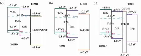
Device C showed the highest efficiency among the three devices. Compared with CzSi, the energy barriers of the highest occupied molecular orbital(HOMO) levels of Tm3PyP26PyB, TmPyPB and TPBi were 0.5, 0.7, 0.2 eV, respectively, indicating that device B had the best hole blocking ability. In addition, the triplet energies of Tm3PyP26PyB, TmPyPB and TPBi are 2.8, 2.9, 2.7 eV, respectively, which strongly influence device performances[19-20]. The low triplet energy may reduce the effect of confining triplet state excitons within the EML. However, DPEPO in device C acts as a HBL and has a high triplet energy(ET=3.0 eV), which improving the efficiency but also increasing the turn-on voltage. To better understand the mechanisms of performances improvement in these devices, as shown in Fig.6, the distribution of carriers within the EML of these devices was also analyzed. The experimental results showed that electron mobility has great effect on efficiency of the devices[21]. For these devices, the electron mobility of Tm3PyP26PyB(2.76×10⁻⁴cm2·V-1·s-1), TmPyPB(~10-5cm2·V-1·s-1) and TPBi(5.6×10⁻⁸-2.1×10⁻⁵cm2·V-1·s-1) decreases successively[22-24], meaning decreasing electrons within EML under the same conditions. Luminance of device C was lower than those of devices A and B. However, electrons and holes tended to balance in device C and decreasing electron mobility causes the shift of recombination center towards cathode, thus resulting in widening the recombination zone and suppressing the annihilation of excitons within EML.

Fig.6 Carriers’ distribution of devices A(a), B(b) and C(c)(Symbols ‘-’ and ‘+’ represent electrons and holes, respectively).
Therefore, device C realized the highest efficiency.
4 Conclusion
This work demonstrated that the efficiency of device could be improved by designing mixed-host structure and optimizing the selection of electron transport material. High efficiency blue devices prepared by solution method were achieved by constructing mixed-host structure with the combination of high triplet energy host material with high hole mobility host material. EL efficiency was further improved by selecting a suitable electron transport material. In this case, carriers tended to balance, thus improving device efficiency and reducing exciton quenching. The optimal device with TcTa∶CzSi of 6∶1 and 70 nm TPBi layer displayed theBmax, CEmax, PEmaxand EQEmaxof 6 662 cd·m-2, 39.40 cd·A-1, 23.33 lm·W-1and 19.7%, respectively.
Response Letter is available for this paper at:http://cjl.lightpublishing.cn/thesisDetails#10.37188/CJL.20220049.
杂志排行
发光学报的其它文章
- A Simple Method to Enhance Performance of Inverted Planar Perovskite Solar Cells by Using PEDOT∶PSS Doped with DMSO as Hole Transport Layer
- Optimal Doping Content of Red Emitting Y4GeO8∶Bi3+,Eu3+ Phosphor Designed by Response Surface Methodology
- 低温808 nm高效率半导体激光器
- Sn2+-Mn2+共掺杂Gd2O3-Al2O3-SiO2玻璃光致发光性能与能量传递
- 硫化锌电致发光材料在智能可穿戴领域研究进展
- 电子阻挡层Al组分对GaN基蓝光激光二极管光电性能的影响
