DC and analog/RF performance of C-shaped pocket TFET(CSP-TFET)with fully overlapping gate
2022-05-16ZiXinChen陈子馨WeiJingLiu刘伟景JiangNanLiu刘江南QiuHuiWang王秋蕙XuGuoZhang章徐国JieXu许洁QingHuaLi李清华WeiBai白伟andXiaoDongTang唐晓东
Zi-Xin Chen(陈子馨) Wei-Jing Liu(刘伟景) Jiang-Nan Liu(刘江南) Qiu-Hui Wang(王秋蕙)Xu-Guo Zhang(章徐国) Jie Xu(许洁) Qing-Hua Li(李清华) Wei Bai(白伟) and Xiao-Dong Tang(唐晓东)
1College of Electronics and Information Engineering,Shanghai University of Electric Power,Shanghai 200090,China 2GTA Semiconductor Corporation Limited,Shanghai 200123,China
3Key Laboratory of Polar Materials and Devices,East China Normal University,Shanghai 200041,China
Keywords: tunnel field effect transistor,double gate,pocket
1. Introduction
As the feature size of metal oxide semiconductor field effect transistors (MOSFETs) continues to decrease, the supply voltage (VDD) scaling of MOSFETs will be quite slow.With the increasing reduction of technology nodes, the lack ofVDDscaling has recently led to power consumption problems because MOSFETs are approaching to their minimumVDDdetermined by the operating mechanism. Thus, higher device power consumption will become a major constraint on the transistor performance. To meet the demand for lowpower circuits in the era of big data, many researchers have proposed a variety of ultra-steep subthreshold swing devices based on novel operating mechanisms, including piezoelectric field-effect transistors(piezo-FETs),negative capacitance field-effect transistors (NC-FETs), and tunneling field-effect transistors(TFETs). TFETs are emerging as a promising candidate for ultra-low power applications due to their advantages of low leakage currents, low temperature dependence,and low sub-threshold swings,which can be achieved beyond the 60 mV/dec limit of MOSFETs at room temperature.[2–9]However, the drawbacks of TFETs are low on-state current and the occurrence of ambipolar current. Many researchers addressed these problems by means of modifying the device structure,such as the use of dual-gate TFETs,[2,10]gate-all-around TFETs,[11,12]L-shaped gate TFETs[13,14]and gate–source/drain overlapping,[15,16]or adopting different kinds of materials such as hetero-gate dielectric,[17–19]III–IV materials[20–22]and hetero-material gate.[23,24]The low on-current of the silicon-based TFETs are an inherent difficulty in Si due to the indirect bandgap and low tunneling effective mass.[25]In order to achieve a higher on-state current of the silicon-based TFETs, the source-pocket TFET(PNPN-TFET)[26–30]has recently been proposed, which features a heavily doped N pocket added on the source side,leading to enhanced on-state currents,[26]improved on/off current ratios and steep subthreshold swings compared with the conventional PIN-TFETs. Different structures and materials of pocket in PNPN-TFETs have been explored: (1) vertical pocket inserted between the source and channel based on the fully depleted pocket region,which results in reducing the tunneling width and then enhancing the lateral electric field at the tunneling junction;[26,27,30](2)horizontal pocket added on the source side based on the line tunneling-based structures;[29,31](3)the use of SiGe pocket materials[32,35]due to its VLSI compatibility and tunable bandgap. In addition, a gate-to-pocket overlapping structure has been demonstrated as a new way to enhance the BTBT generation rate and thus to improve the tunneling current.[33]However, the silicon-based TFETs still require further improvements in terms ofIonand subthreshold swing(SS)for ultra-low power applications.
In this work, the silicon-based double-gate PNPN-TFET with symmetrical horizontal pocket and gate-to-pocket overlapping structure — silicon-based C-shaped pocket TFET(CSP-TFET) has been proposed to further improve the onstate current and subthreshold swing. The effect of the physical dimensional parameters and the doping concentration of the pocket on the DC and analog/RF performance of the CSPTFET device are analyzed in detail. The experimental details will be explored in the following sections. Section 2 describes the basic structure, parameters, simulation models, and calibration experiments of the proposed device. Section 3 discusses the characteristics of the structure and the optimization process, and then Section 4 summarizes the article with relevant notes.
2. Device structures,parameters,simulation details and calibration
The simulated CSP-TFET is schematically presented in Fig. 1, and the specific parameters of the device are shown in Table 1. The doping concentrations of the source, channel, and drain are 1×1020cm-3(for p-type), 1×1017cm-3(for p-type), and 5×1018cm-3(for n-type), respectively.All regions are assumed to be uniformly doped. The PNPNTFETs are characteristically based on the conventional structure of silicon-based double-gate TFETs with a heavily Ndoped pocket incorporated between the source and channel.The principle of the PNPN-TFET is to make the pocket region fully depleted under the applied voltage, increasing the electric field and thus enhancing the band-to-band tunneling rate between the source and channel, which leads to an increase in the on-state current. The proposed CSP-TFET device is based on the N-doped pocket region(region name: pocket 2)between the source and channel, with another pocket region(region name: pocket 1)added to the source. The pocket 1 is connected to the pocket 2. The N-doped pocket 1 and pocket 2 are collectively called the “pocket”, and the entire pocket(including pocket 1 and pocket 2) looks like a “C” shape, as shown in Fig.1. It is assumed that pocket 1 and pocket 2 are consistent in doping concentration. SiO2is used as the gate oxide layer with a thickness of 2 nm. The simulation parameters,such as the length of pocket 1(Lp1),the length of pocket 2(Lp2)and the pocket doping concentration(Np),will be used as variables. Assuming that the pocket is fully covered by the gate. The work functionφ(of the gate) is set to be 4.5 eV.In addition to studying the effect of pocket length and doping concentration on the DC and analog/RF properties of the CSP-TFET device, the influence of the gate position of the CSP-TFET device is also investigated.
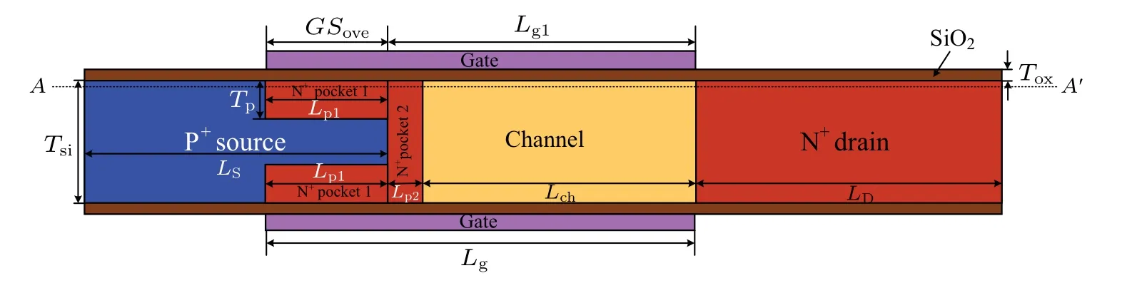
Fig.1. The 2-D schematic view of CSP-TFET.
Table 1. Device parameters.
The CSP-TFET is investigated by using Synopsys Sentaurus TCAD. The meshes need to be carefully defined to accurately extract data, especially for the interface between source and pocket and the interface between pocket and gate oxide layer. Since the source and drain of TFET are heavily doped,the Fermi–Dirac model and the bandgap narrowing model are employed. The doping-dependent mobility model,the carrier Shockley–Read–Hall(SRH)model,and the Auger model are also adopted. Since the silicon thickness (Tsi) is 20 nm (larger than 7 nm), quantum effects are not considered in this simulation. The common band-to-band tunneling models include Schenk, Hurkx, the simple band-to-band tunneling model and the dynamic nonlocal path band-to-band tunneling (BTBT) model. The electric field and the carrier distribution at each point of the actual tunneling path are not constant. This paper employs the dynamic non-local BTBT model,which is the most versatile model and becomes a more flexible and convenient way to deal with arbitrarily shaped potential barriers. When using a nonlocal dynamic band-toband tunneling model,the default values of the model parameters are inaccurate and need to be calibrated based on experimental results. The nonlocal BTBT model used in this paper is calibrated by using the work by Boucart and Ionescu.[1]The phonon-assisted factors(Apath1=4.0×1016cm-3·s-1andBpath1=1.9×10⁷MV·cm-1)are chosen for silicon materials to achieve the best fitting results. The tunneling model used has been calibrated with the reported results.[1]The calibration of transfer characteristics is depicted in Fig.2.
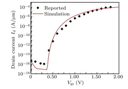
Fig.2.Calibration of the TCAD model parameters obtained by comparing the simulated and experimental Ids–Vgs characteristics of Ref.[1].
3. Results and discussion
Pocket length, pocket doping concentration and gate position are discussed for better DC and analog/RF performance.TheIon,Ioff,Ion/Ioff,andSSavgare used as important indicators of the DC characteristics, and subsequently, thegm,fT, and GBP are used as those of the analog/RF characteristics. The drain voltageVdis set to be 1 V. The gate voltageVgvaries from 0 to 2 V.The on-state current(Ion)and the off-state current(Ioff)are defined by the drain currents(Id)underVd=1 V withVg=2 V andVg=0 V.
3.1. Effect of Lp2 and Np
Figure 3(a)shows the transfer characteristics with different value ofLp2of the proposed CSP-TFET at a fixed pocket1 length (Lp1) of 2 nm and a pocket doping concentration (Np)of 1×1020cm-3. Note that in this work,the energy band diagrams are obtained at the location of 1 nm below the interface of silicon and gate oxide layer along the channel direction. As shown in Fig. 3(b) along the lineA–A′in Fig. 1, there is a local minimum in the conduction bandEcof this device depicted in the locally enlarged picture due to the addition of pocket 2 between the source and channel,where the pocket 2 is either fully or partially depleted under the gate voltage.[17]It is observed from Fig.3(a)that the drain currents of the device increase sharply and approach saturation atLp2>2 nm,and the on-state currents atLp2>2 nm are approximately 1.5 times higher than those atLp2≤2 nm. This may be because the local minimum of the conduction band (Ec) in pocket 2 atLp2>2 nm has more energy band overlapping region with the valence band(Ev)in the source,resulting in more electron tunneling from the source into the channel as seen in Fig.3(b).Moreover, Fig. 3(a) shows, without the gate voltage applied,the significant leakage currents were observed in the off state,which degrades severely to about 10-6A/μm atLp2>2 nm,while the drain current atLp2≤2 nm is less than 10-15A/μm.The behavior of the drain currents of the CSP-TFET device in the off-state condition is illustrated by Fig.3(c),where the conduction band in pocket 2 atLp2≤2 nm lies above the valence band in the source in the absence of the gate voltage.The BTBT is suppressed, resulting in the device being in the off state. WhenLp2is greater than 2 nm,the conduction band of pocket 2 region is below the valence band of the source.
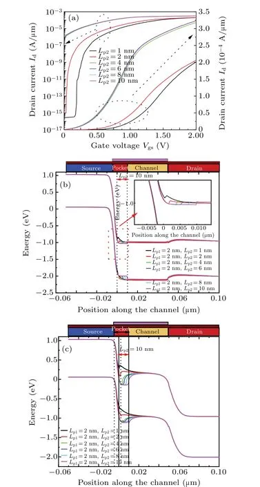
Fig.3. (a)Effect of Lp2 on the transfer characteristics of the CSPTFET device at Lp1=2 nm and Np=1×1020 cm-3(@Vd=1 V,@Vg=2 V),where the left Y-axis is the logarithmic curve and the right Y-axis is the linear curve.(b)Energy band diagram for Lp2 varying from 1 nm to 10 nm in the on-state at Lp1 =2 nm and Np =1×1020 cm-3 (@Vd =1 V, @Vg =2 V), where the box checked by the red dashed line is an enlarged picture between the source and the channel. (c)Energy band diagram for Lp2 varying from 1 nm to 10 nm in the off-state at Lp1=2 nm and Np=1×1020 cm-3 (@Vd=1 V,@Vg=0 V).
Therefore, the conduction band in the pocket 2 and the valence band in the source overlap, and electrons from the source can enter the channel with no gate voltage applied,and thus band-to-band tunneling occurs,as shown in Fig.3(c)along the lineA–A′in Fig. 1. Therefore, for a fixedLp1of 2 nm and a pocket doping concentration of 1×1020cm-3,the device has an on-state current>10-4A/μm, an off-state current<10-15A/μm, andIon/Ioffof approximately 1011atLp2≤2 nm. To further optimizeLp2,the DC and analog characteristics of the device for bothLp2of 1 nm and 2 nm are compared and analyzed.
The calculated DC characteristics (e.g.,Ion,Ioff,SSavg,Ion/Ioff) are shown in Table 2.SSis defined as the change in gate voltage which must be applied in order to create a one decade increase in the output current,[1]defined by (d logId/dVgs)-1in units of mV/decade.[25]In this work, the average subthreshold swing and point subthreshold swing performance metrics are adopted.SSpointis measured around the voltage corresponding to a drain current of 10-7A/μm. Several methods of defining subthreshold swing have been proposed for TFETs.[1,34]Bhuwalka[34]and Boucart and Ionescu[1]have proposed definitions for calculating theSSavg,[25]defined as
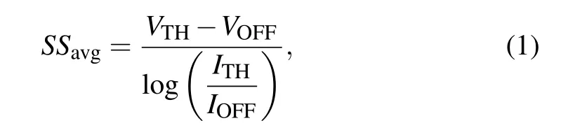
whereVTHis the threshold voltage whose value is the voltage corresponding to a drain currentITHof 10-7A/μm. Since the minimum tunneling current varies in different cases,theVOFFin this work is the voltage corresponding to a drain currentIoffof 10-14A/μm.
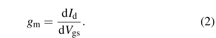
Table 2 shows different DC and analog parameters extracted from the transfer characteristics betweenLp2=1 nm and 2 nm. It is obvious that the numerical results forIonandSSavgatLp2=1 nm are similar to those atLp2=2 nm,while the latter(Ioff=9.509×10⁻¹⁶A/μm forLp2=2 nm)has an off-state current approximately 3.42 times higher than the former(Ioff=2.779×10⁻¹⁶A/μm forLp2=1 nm). Hence,theIon/Ioffof the former(Ion/Ioff=7.247×1011forLp2=1 nm)is three times more than that of the latter(Ion/Ioff=2.166×1011forLp2=2 nm). It is important to add that a critical indicator of the analog characteristics of the device is thegm,which represents the gate controllability over the drain current, i.e.,the relative change in drain current with the change in gate voltage,as shown below:
It can also be found thatgmatLp2=1 nm(3.39×10⁻⁴S)is slightly higher than that atLp2=2 nm (2.68×10⁻⁴S) from Eq. (2) and Table 2. Based on the factors mentioned above,the optimumLp2is found to be 1 nm forLp1= 2 nm andNp=1×1020cm-3.
The pocket doping concentration(Np)also has an impact on the electrical properties of the CSP-TFET device fixingLp1andLp2. From Figs. 4 and 5(a), it can be seen that the on-state current of the device increases by 30.8% when the pocket doping concentration increases from 2×1019cm-3to 1×1020cm-3,and reaches a peak value of 2.01×10⁻⁴A/μm when the pocket doping concentration reaches 1×1020cm-3atLp1=2 nm andLp2=1 nm. This is possibly because in pocket 2, the pocket doping concentration becomes higher,making the pocket region fully depleted, thus leading to an increase in the electric field between the source and channel,and therefore increasing the BTBT current.It is observed from Figs. 4, 5(a) and 5(b) that the off-state currents of the CSPTFET devices increase with the pocket doping concentration butIoff<10-14A/μm, andIon/Ioff>1010. TheSSavgof the device in Fig. 5(b) continue to decrease with increasingNp,decreasing by~18 mV/dec, which can be reflected in the transfer characteristics in Fig. 4. It can be clearly seen that the higher theNpis, the steeper the slope of the curve in the subthreshold region becomes,which leads to the faster switching speed of the CSP-TFET device. Thus,there exists an optimum pocket doping concentration (Np) of 1×1020cm-3atLp1=2 nm andLp2=1 nm for better DC characteristics.
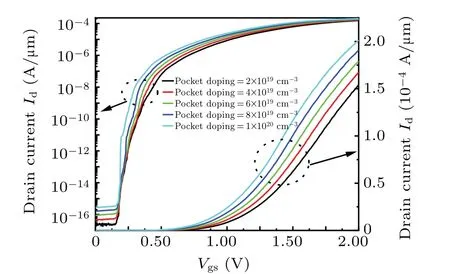
Fig.4. Effect of pocket doping concentration variation on transfer characteristics at Lp1 =2 nm and Lp2 =1 nm (@Vd =1 V, @Vg =2 V),where the left Y-axis is the logarithmic curve and the right Y-axis is the linear curve.
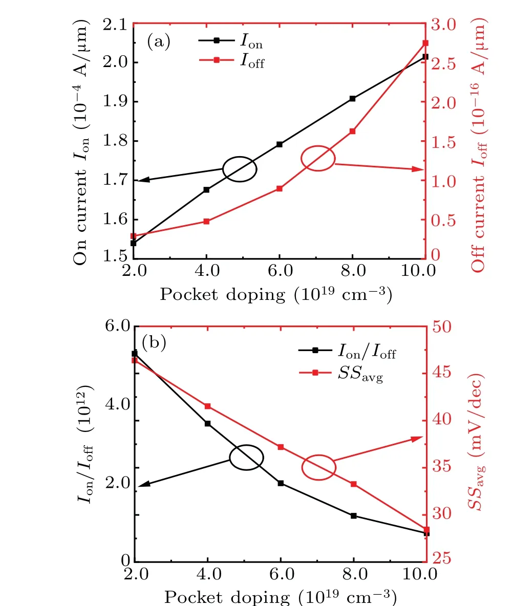
Fig.5. Impact of pocket doping concentration variation on(a)Ion and Ioff;(b)Ion/Ioff and SSavg at Lp1=2 nm and Lp2=1 nm.
3.2. Effect of Lp1
The effect ofLp1on the DC and analog/RF characteristics of the CSP-TFET device is investigated for a fixed optimum value ofNp=1×1020cm-3andLp2=1 nm.
3.2.1. DC characteristics
The effect ofLp1on the transfer characteristics of the device is shown in Fig. 6. The linear curves in Figs. 6 and 8 reveal that asLp1increases from 2 nm to 30 nm,the curve in the subthreshold region of the transfer characteristics becomes steeper. TheSSavgdecreases by approximately 16 mV/dec,while the on-state current increases by about 8.0×10⁻⁴A/μm.The off-state current also becomes larger with an increase ofLp1, with an upper limitation of 10-14A/μm. Hence,Ion/Ioffis still greater than 107.
The experiment begins with a default gate position that completely covers the pocket and the channel. The effect of the gate position on the CSP-TFET device will be discussed later in Subsection 3.2. Figure 7 shows the comparison of the physical electric field diagrams and electron BTBT tunneling rate diagrams withLp1of 2 nm and 30 nm, respectively, for a given gate bias. Figures 7(b)and 7(d)show that the longer theLp1is,the more the gate and pocket regions overlap,which leads to in the electric field extending towards the source,i.e.,tunneling electrons are generated vertically and horizontally along pocket 2,which leads to more electrons being collected by the drain. Thus, the optimized DC characteristics of the device is found atLp1= 30 nm. In this case, the average subthreshold swing is 12.19 mV/dec, the transconductance is 1.268×10⁻³S, the on-state current is 9.98×10⁻⁴A/μm, the off-state current is 3.681×10⁻¹⁵A/μm, and theIon/Ioffis 2.71×10¹¹.
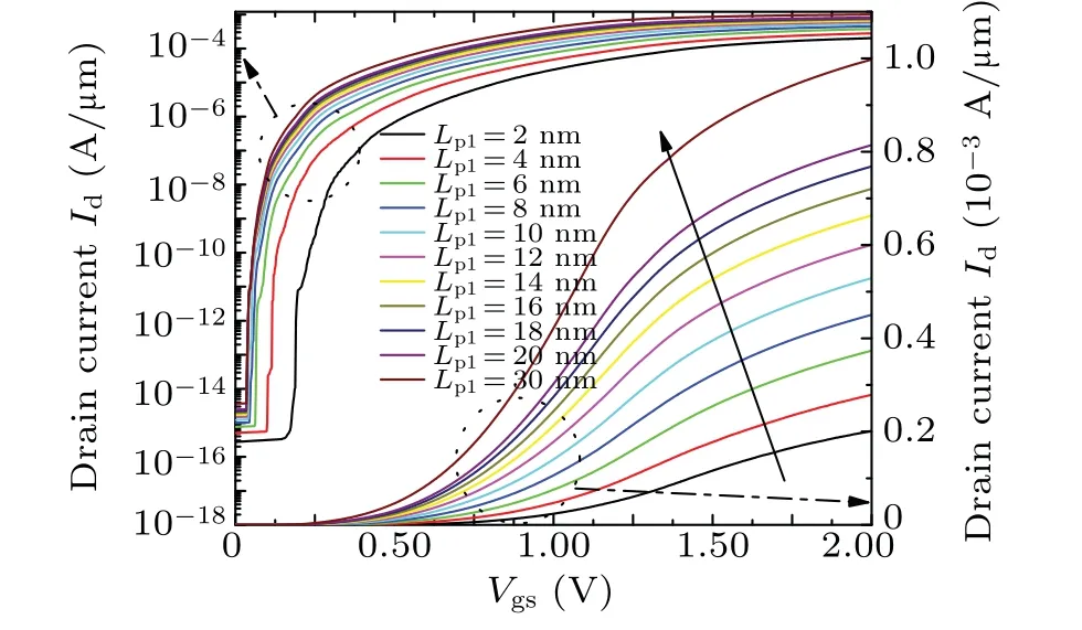
Fig.6. Effect of Lp1 variation on transfer characteristics of the device at Lp2=1 nm and Np=1×1020 cm-3 (@Vd=1 V,@Vg=2 V),where the left Y-axis is the logarithmic curve and the right Y-axis is the linear curve.
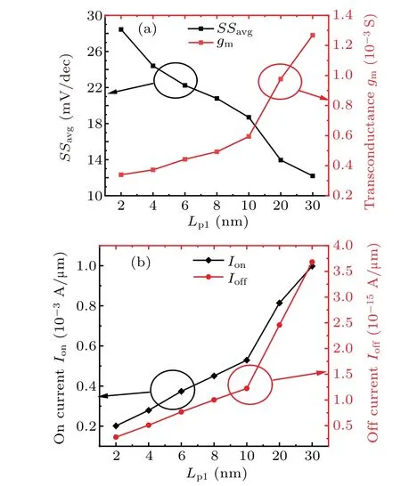
Fig. 8. Impact of Lp1 variation on (a) SSavg and gm; (b) Ion and Ioff at Lp2=1 nm and Np=1×1020 cm-3.
3.2.2. Analog/RF characteristics
Having investigated the DC characteristics, this section evaluates the analog/RF characteristics of the CSP-TFET device. The simulated performance parameters are analyzed by using an AC analytical method, and the capacitance parameters are extracted at an operating frequency of 1 MHz frequency conditions. Thegmis an important indicator to measure the analog characteristics of devices,[35]and a highergmmakes the device beneficial for analog applications. Analysis of the analog parametergmplays a critical role in obtaining higherfTand GBP.[36]The transconductance is defined as Eq. (2). Figure 9(a) shows the transconductance of the CSP-TFET device with differentLp1and it is shown that the maximumgm(gm,max) of the CSP-TFET device is 1.268×10⁻³S atLp1=30 nm. Furthermore,gmis increased withVgs, forVgsbelow 1 V, beyond whichgmstarts to decrease atLp1=30 nm.The decrease ingmaftergmreaches thegm,maxis probably caused by carrier velocity saturation at high electric fields,leading to the degradation of the carrier mobility. Figures 9(b)–9(d)show the variation of the gate-to-source capacitance(Cgs), the gate-to-drain capacitance(Cgd) and the gate capacitance (Cgg=Cgs+Cgd) withVgsforLp1ranging from 2 nm to 30 nm. The capacitance parameters also have influence on thefTand GBP,which will be discussed later. The cut-off frequency,which is the frequency at which the current gain becomes unity,plays a significant role in deciding the device performance at high frequency,[37]as shown below:
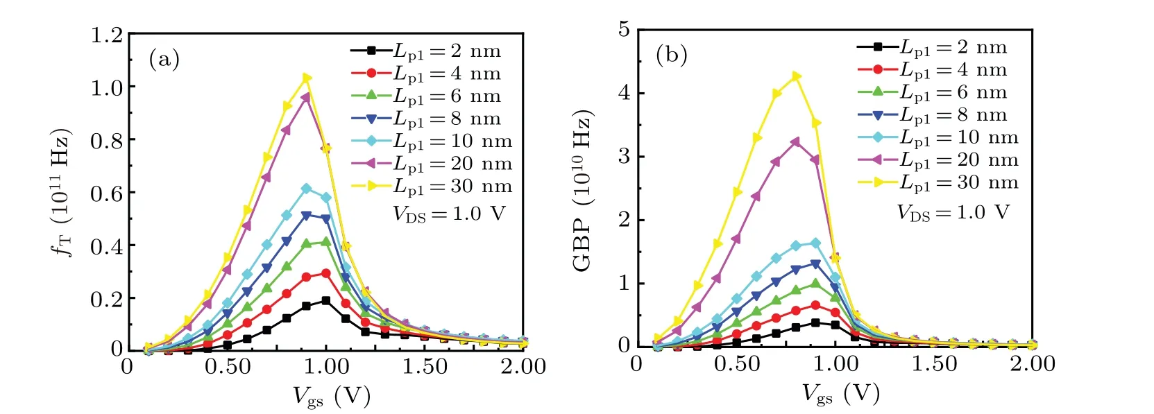
Fig.10. Variation of(a) fT and(b)GBP with different Lp1 from 2 nm to 30 nm.
Figure 10(a) shows the variation offTwithVgsasLp1ranges from 2 nm to 30 nm. It is observed from Eq. (3)thatfTis proportional togmand inversely proportional toCgg. Note thatCggremains at a small value for all curves whenVgs<0.9 V and then increases rapidly withVgs, whenVgs>0.9 V in Fig.9(b). The cut-off frequency variation withVgswhenVgs>0.9 V,as shown in Fig.10(a),decreases sharply after reaching the maximum cut-off frequency(fTmax)becausegmdecreases withVgsandCggincreases withVgs,which leads to a faster rate offTdecline. Figure 10(a) shows that asLp1increases to 30 nm, the CSP-TFET device shows the highest cut-off frequency of 1.0316×10¹¹Hz whenVgs=0.9 V.GBP is another significant parameter,which represents the product of gain and bandwidth of the active device or circuit.The value of GBP is expressed as follows:
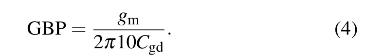
From Eq. (4), GBP is still proportional togmand inversely proportional toCgd. Figure 10(b)shows the variation of GBP withVgsasLp1ranges from 2 nm to 30 nm and the trend of GBP is basically the same as Fig. 10(a). Thus, the GBP achieves a maximum value of 4.266×10¹⁰Hz whenLp1=30 nm.
3.3. Effect of the location of the gate
Based on the discussion above, the optimalLp1,Lp2andNpof the proposed CSP-TFET device are selected as 30 nm,1 nm and 1×1020cm-3, respectively. In order to investigate the effect of gate-to-pocket overlapping structures on the electrical properties of the device, we simulate 6GSoves: 3 nm,6 nm,12 nm,18 nm,24 nm,and 30 nm(in this work,we defineGSoveasL×Lp1and simulate 6Ls: 0.1,0.2,0.4,0.6,0.8,and 1.0 for a fixed optimumLp1value of 30 nm),which represent the length of the overlapping region between the gate and pocket 1.Lis the gate-to-pocket overlapping factor.
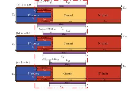
Fig.11. Structure diagrams of the variation of L ranging from 0.1 to 1.0.
Figure 11 shows the structure diagram of the CSP-TFETs with the change ofL(1.0,0.6,and 0.1). For 0<L ≤1,L=1 represents the gate fully overlapping the pocket region(including pocket 1 and pocket 2) and 0<L <1 denotes the gate partially overlapping of the pocket region.

Fig. 12. Effect of L (the change in position of the gate) on the transfer characteristics of the CSP-TFET at Lp1 = 30 nm, Lp2 = 1 nm,Np=1×1020 cm-3 (@Vd=1 V,@Vg=2 V),where the sitting Y-axis is a logarithmic curve and the right Y-axis is a linear curve.

Fig. 13. Impact of L variation on (a) SSavg and SSpoint; (b) gm and Ion/Ioff;(c)Ion and Ioff.
Figure 12 shows the effect ofLon the transfer characteristics of the CSP-TFET device. Figures 13(a)–13(c) illustrate the DC and transconductance parameters extracted from Fig.12. Figure 13(a)showsSSavgandSSpointas a function ofL. It can be seen that bothSSavgandSSpointdecrease asLincreases, withSSavgimproving by 10.342 mV/dec andSSpointdecreasing by 53.7 mV/dec. Figure 13(b)shows the variation ofgmandIon/IoffasLranges from 0.1 to 1.0. ForL=1.0,the device has the maximum value in terms ofgmandIon/Ioffand shows better gate controllability and switching capability. Moreover, Fig.13(c)showsIonandIoffvary withL. It is clear that the on-state current improves by 7.834×10⁻⁴A/μm whenLincreases from 0.1 to 1.0. According to Figs. 12 and 13, forL=1.0, i.e., fully gate-to-pocket overlapping structure,the CSP-TFET device has the smallestSSavgandSSpoint,the largestIon,Ion/Ioff, andgm, which has the optimized DC and analog characteristics.
4. Conclusion and perspectives
In this paper,a C-shaped pocket TFET with the gate covering the pocket based on the double-gate TFET is proposed and analyzed. The pocket is C-shaped which is incorporated between source and channel to enhance device performance.The pocket length and pocket doping concentration affect the DC and analog/RF performance of the C-shaped pocket TFET.The use of fully gate-to-pocket overlapping structure results in the improvements of gate controllability and current driving capability. Our results demonstrate that high pocket doping concentration (Np) and narrow pocket 2 length (Lp2) can achieve better electrical properties. The increase in pocket 1 length(Lp1)results in a larger overlapping region between the gate and pocket, which increases the electric field, and then increases the BTBT rate of the electrons. The silicon-based double-gate CSP-TFET demonstrated superior DC and analog/RF performance withIon=9.98×10⁻⁴A/μm,SSavg=12.19 mV/dec,SSpoint=52.81 mV/dec,gm=1.268×10-3S,Ion/Ioff= 2.71×10¹¹,fT= 1.0316×10¹¹Hz and GBP =4.266×10¹⁰Hz atLp1= 30 nm,Lp2= 1 nm andNp=1×1020cm-3. The results of this work indicates that the CSP-TFET device is suitable for high speed and low power applications.
Acknowledgements
Project supported by the National Natural Science Foundation of China (Grant Nos. 52177185 and 62174055) and Open Fund of Shanghai Key Laboratory of Multidimensional Information Processing,East China Normal University(Grant No.2019MIP002).
猜你喜欢
杂志排行

Chinese Physics B的其它文章
- Erratum to“Boundary layer flow and heat transfer of a Casson fluid past a symmetric porous wedge with surface heat flux”
- Erratum to“Accurate GW0 band gaps and their phonon-induced renormalization in solids”
- A novel method for identifying influential nodes in complex networks based on gravity model
- Voter model on adaptive networks
- A novel car-following model by sharing cooperative information transmission delayed effect under V2X environment and its additional energy consumption
- GeSn(0.524 eV)single-junction thermophotovoltaic cells based on the device transport model