Robustness of the unidirectional stripe order in the kagome superconductor CsV3Sb5
2022-05-16BinHu胡彬YuhanYe耶郁晗ZihaoHuang黄子豪XiangheHan韩相和ZhenZhao赵振HaitaoYang杨海涛HuiChen陈辉andHongJunGao高鸿钧
Bin Hu(胡彬) Yuhan Ye(耶郁晗) Zihao Huang(黄子豪) Xianghe Han(韩相和) Zhen Zhao(赵振)Haitao Yang(杨海涛) Hui Chen(陈辉) and Hong-Jun Gao(高鸿钧)
1Institute of Physics and University of Chinese Academy of Sciences,Chinese Academy of Sciences,Beijing 100190,China
2CAS Center for Excellence in Topological Quantum Computation,Beijing 100190,China
3Songshan Lake Materials Laboratory,Dongguan 523808,China
Keywords: CsV3Sb5, 4a0 stripe charge order, scanning tunneling microscopy/spectroscopy, charge density wave,
1. Introduction
Kagome lattice, composed of corner-sharing triangles,hosts a fascinating electronic band with Dirac cones,flat band and van Hove singularities.[1—3]Materials with kagome lattice provide an important platform to study diverse kinds of electronic states such as quantum spin liquid,[4]density waves,[5,6]and unconventional superconductivity.[6,7]Especially, magnetic Weyl semimetal phase,massive Dirac fermions and large anomalous Hall effect have been observed on the transitionalmetal-based kagome system Co3Sn2S2,[8—10]Fe3Sn2,[11—13]Mn3Sn,[14,15]and ReMn6Sn6.[16,17]Recently, a new family of layered kagome metalsAV3Sb5(A= K, Rb or Cs)has been discovered to hostZ2nontrivial topological band structure[18,19]and possible Majorana zero mode.[20]Moreover,AV3Sb5exhibits giant anomalous Hall effect,[21—23]unconventional superconductivity,[24—26]and pair density wave,[24]serving as an ideal platform to study the emergent electronic states.
In the family ofAV3Sb5, both theory and experiments confirm that there exists a charge density wave(CDW)transition at 80—110 K.[18,27—31]The CDW,which breaks the lattice translational symmetry and potential time-reversal symmetry and whose modulation alongcaxis breaks the rotational symmetry,tantalizes enough research interest among the study ofAV3Sb5.[18,22,24,27—36]The CDW inAV3Sb5coexists with the unconventional superconductivity and other exotic states like pair density wave[24]at low temperature. So far,two types of orders including the charge order with 2a0period propagating along all lattice directions (2×2) and unidirectional 4a0stripe order are reported on the Sb surface of RbV3Sb5and CsV3Sb5[20,24,28,29,31,33—35,37,38]and only the 2×2 CDW order is observed on the Sb surface of KV3Sb5.[28,32,36]Although comprehensive studies have demonstrated the existence of 2×2×2 or 2×2×4 CDW in the bulk,[20,24,28,29,31—37]there are few works on the identifications of 4a0stripe order.[20,24,31,34]Moreover, the mechanism of unidirectional stripe order remains elusive and the CDW origin of 4a0is controversial. Although many works attribute the 4a0stripe order to the CDWinduced modulation,[24,31,39]a few works argue that the 4a0modulation is from in-plane shifting of atoms and fragile because of surface origin.[34,40]
Here, we systematically study the 4a0stripe order in CsV3Sb5by using low-temperature scanning tunneling microscopy/spectroscopy (STM/S). We find that the nondispersive 4a0unidirectional order exists among a large energy scale. The intensity of the 4a0unidirectional modulation is converse in the STM image with negative and positive bias. Furthermore,this stripe order can persist across the step edges, point defects, and strains, under strong magnetic fields and temperature below~60 K. All these features are in consistence with the STM observations of a well-known robust CDW in other materials. Our results provide a strong experimental evidence on the robust existence of the unidirectional 4a0stripe charge order in the kagome superconductor CsV3Sb5.
2. Methods
The CsV3Sb5sample was grown from Cs liquid (purity 99.98%), V powder (purity 99.9%) and Sb shot (purity 99.999%)via a modified self-flux method.[18,24]The samples used in the experiments were cleaved at about 10 K and immediately transferred to an STM chamber. Experiments were performed in an ultrahigh-vacuum(1×10⁻¹⁰mbar)low temperature STM system equipped with a 9-2-2 T magnetic field.All of the scanning parameters (setpoint voltage and current)of the STM topographic images are listed in the figure captions. Tungsten tips used in the experiment were fabricated via electrochemical etching and calibrated on a clean Au(111)surface prepared by repeated cycles of sputtering with argon ions and annealing at 500°C.
3. Results and discussion
As shown in Fig. 1(a), CsV3Sb5has a hexagonal symmetry structure (space groupP6/mmm,a=b=5.4 °A,c=9 °A), consisting of periodic stacking layers: Cs—Sb2—VSb1—Sb2—Cs. The middle layer in the lattice, VSb1 layer, has a vanadium-based kagome net interpenetrated with hexagonal structured Sb1. This intriguing kagome layer is sandwiched by two honeycomb Sb2 layers, and all these three layers are between two simple hexagonal Cs layers. As the chemical bonding between Cs and Sb2 slab is weaker than that between Sb2 and VSb1,the cleavage procedure always produces Cs or Sb terminated surfaces. The terminated surface can be easily identified by its structure because the Cs surface has a hexagonal lattice while the Sb surface has a honeycomb lattice(small light blue circles in Fig.1(b)). The unidirectional stripe order with a two-fold symmetry is observed on the Sb terminated surface rather than Cs layer, thus we focus on the Sb surface in the following studies.
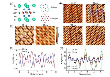
Fig. 1. Bias-dependent STM images of unidirectional 4a0 charge orders on the Sb-terminated surface of CsV3Sb5 at 4.2 K. (a) Schematic of CsV3Sb5 crystal structure(right)and atomic structures of VSb layer and Sb layer(left). (b)STM images of Sb-terminated surface at the sample bias of -20 mV, -50 mV, -100 mV and -500 mV, respectively (It =2.0 nA). Blue circles highlight the Sb atoms positions with hexagonal symmetry and correspond to Sb2 layer. The topography size is 7 nm×7 nm. (c)Line profiles along the black arrow in the four STM images of(b),showing that the protrusions of 4a0 modulation depend on the scanning bias. (d)STM image of the same Sb-terminated surface at+60 mV and-60 mV,respectively, showing the inversion of intensity contrast. The point defect highlighted by the white dotted circle marks the same spatial spot (Vs =-60 mV, It =0.5 nA for the left panel;Vs =+60 mV, It =0.5 nA for the right panel). (e) Line profiles along the two arrows in (d),showing the peak-to-dip intensity contrast for the STM image with positive and negative scanning bias. The topography size is 11 nm×11 nm.
To study the influence of the scan bias on the stripe order period, we collect a series of STM images with different scan bias. At the bias ranging from-500 mV to 0 mV, all the STM images show a unidirectional spatial modulation as highlighted by the light blue shades.The periodicity of spatial modulation responding to the shade is about 2.5 nm, in consistence with the 4a0unidirectional order in the literature.[20,24,31,34]Furthermore,line profiles along the 4a0direction (colored lines) in each STM image in Fig. 1(b) show that, the spatial modulation of the 4a0stripe order manifests itself more significantly at lower bias (Fig. 1(c)). By switching the scan bias from negative value to positive value but keeping other parameters the same, we find that the two STM images of the same region with the opposite scan biases have a contrast inversion, which has been demonstrated to be the hallmark for the Peierls-type CDW.[41—44]Line profiles taken along colored arrows perpendicular to the stripe direction in Fig. 1(d)are shown in Fig. 1(e), where the peak-to-dip feature can be clearly seen. By a close inspection of the contrast, we can calculate the normalized cross correlation coefficient (N=(ai j-¯a)(bi j-¯b)/(σaσb),where ¯a,¯bandσa, σbare means and standard deviations of imagesai j,bi j)of the two images in Fig. 1(d), where lowerNvalue reflects bigger contrast inversion. The result isN~-0.6,indicating high anti-correlation of these two images again. The contrast in the STM images at various scan bias provides strong evidence on the CDW nature of the 4a0stripe order.[20,24,31,34]
Next, in order to study the influence of topmost Cs adatoms on the strength of the 4a0stripe order, we collect a series of STM images on Sb surface with distinct Cs adatom coverage(coverage=the area of Cs adatoms/the area of total field of view=the amount of red pixels/the amount of all pixels in the image)as shown in Fig.2. On the clean Sb surface with low Cs adatom coverage,the long-range 4a0stripe orders are clearly observed as marked by white arrows (Figs. 2(a)and 2(b)). For the regions with higher Cs adatoms coverage,4a0stripe orders are still visible as indicated by yellow arrows in both large-size stereograms (left panels in Figs. 2(c) and 2(d)) and small-size STM images (right panels in Figs. 2(c)and 2(d)). This indicates that the unidirectional order is robust against the Cs adatoms on the Sb surface. It is worthy to notice that the modulations of the 4a0stripe order in the regions with larger Cs adatom coverage are weaker than the ones with lower coverage.[20]We attribute this phenomenon to the following reasons. First, compared to the clean Sb surface, the strong electronic state from the Cs adatoms makes the intensity of the 4a0stripe modulation relatively weaker. Second,a small scan bias will cause the movement of Cs adatoms by the STM tip.[24]Therefore,a large scan bias is always applied for imaging a clear STM topography when the Sb surface is covered with a large amount of Cs adatoms, which will result in the much weaker 4a0stripe order intensity in the STM image(Fig.1(c)). In addition,the Sb surface will be smeared out by the Cs adatoms when the coverage becomes larger,making it difficult to observe this stripe order on the Sb surface.
To study the robustness of the 4a0stripe order against intrinsic defects, we collect the STM images in the regions with different kinds of defects: step edges, strains,and point defects, as shown in Fig. 3. Figure 3(a) shows a two-unit-cell edge (height is~2.0 nm) connecting two clean Sb surfaces. The three-dimensional (3D) plot of the STM image clearly shows that the 4a0unidirectional order keeps continuous across the step edge. Moreover, the orientation of the stripe order does not change across the edge. Except for the step edge, we also observe the 4a0unidirectional order in regions with strains. In a region with strain, there exists non-negligible height protrusion as highlighted by the irregular white hump and the red plateau in the STM image (Fig. 3(b)). However, the stripe order,from top left to bottom right, is immune to the strain effect and evenly distributed. After extensive STM measurements,we find that most regions of Sb surfaces have some randomlydistributed point defects,as shown in Fig.3(c). When the 4a0stripe order encounters the point defects,it will directly cross them instead of changing direction or disappearing. At the same time,the 4a0stripe order is also unchanged when meeting the standing waves induced by the point defects. In short,these results clearly demonstrate that the unidirectional 4a0stripe order is robust against the step edges, strains and point defects.
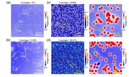
Fig.2. Unidirectional 4a0 stripe order in the Sb surface regions with distinct Cs adatom coverage. (a)Clean Sb-terminated surface(Vs=-90 mV,It =0.05 nA).(b)Sb-terminated surface with 1.55%coverage of Cs atoms(Vs =-50 mV,It =3 nA).(c)—(d)Stereographic STM images of Sbterminated surface with 8.99%and 35.21%coverage of Cs atoms,respectively. Right panels are two corresponding enlarged 2D images in the same region. The 4a0 stripe orders are clearly visible.Vs=-90 mV,It=0.05 nA for(c);Vs=-75 mV,It=0.05 nA for(d).
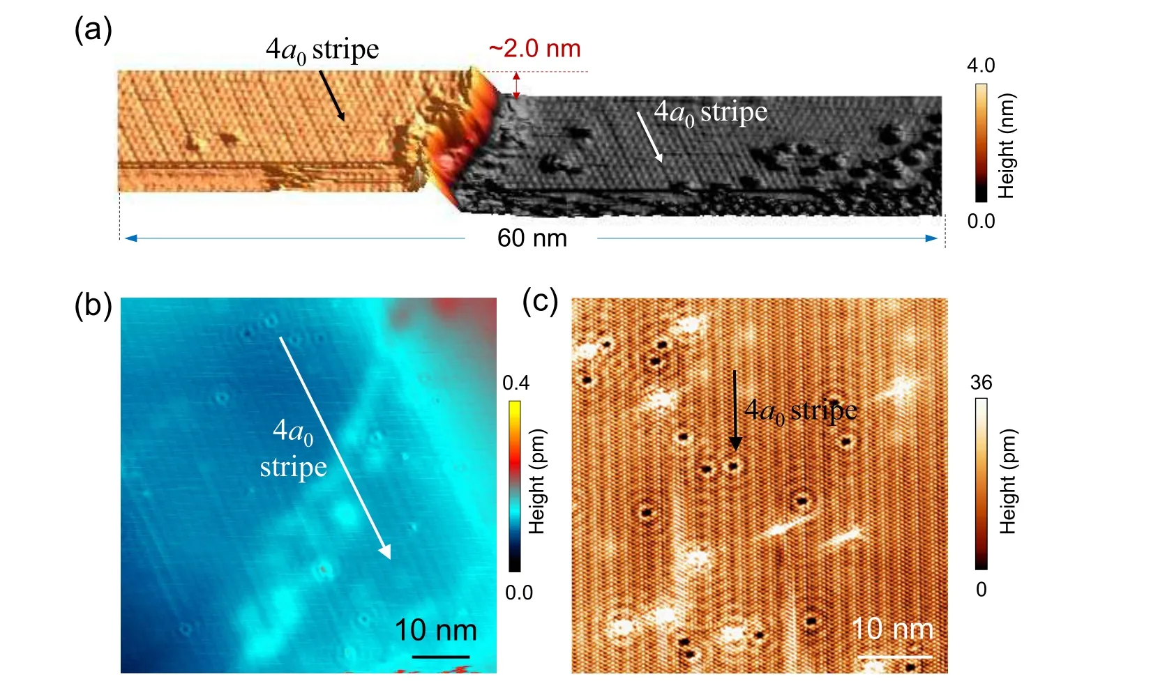
Fig.3. Unidirectional 4a0 stripe order in the Sb surface regions with step edges,strains,or defects. (a)3D image of STM topography showing there is a 2 nm-height edge on Sb surface,showing that the 4a0 stripe order keeps continuous across the step edge(Vs =-50 mV,It =1 nA).(b)STM image of clean Sb surface with strains, indicating the 4a0 modulation is not affected by the strain (Vs =-50 mV, It =5 nA). (c) STM image of clean Sb surface covered with some point defects,showing that 4a0 stripe order is robust across the point defects(Vs=-50 mV,It=1 nA).

Fig. 4. STM images of Sb surfaces acquired at various temperature and magnetic field perpendicular to the surface. (a)—(d) Topography images scanned at 0.8 K, 12 K, 26 K and 76 K, respectively. The 4a0 charge order keeps unchanged at the temperature <26 K but disappears at 76 K(Vs=-5 mV,It=1 nA).(e)—(f)Topography images scanned by applying the magnetic field of 0 and 8 T,respectively,showing that the 4a0 charge order is robust against the applied magnetic field(Vs=-5 mV,It=1 nA).
Finally,we study the effect of temperature and magnetic field on the existence of the 4a0stripe order. Figures 4(a)—4(d) show the STM images of clean Sb surfaces at 0.8 K,12 K,26 K and 76 K,respectively. The 4a0stripe orders are clearly visible in the former three STM images but disappear at 76 K, indicating that the stripe order can persist below the critical temperature at~60 K, consistent with the previous results.[24,31]Furthermore, we vary the magnetic field in the same region of a clean Sb surface at 50 mK. As shown in Figs. 4(e)—4(f), we obtain the STM image at zero magnetic field at first, then increase the magnetic field to 8 T, eventually lower the magnetic field back to zero. During the whole process,the 4a0order remains unaffected. It should be noted that in the temperature dependent and magnetic field dependent experiments,the unidirectional order keeps robust against the point defects.
We notice that although some works have suggested that the 2×2 CDW breaks the time-reversal symmetry(TRS)and further connects to the giant anomalous Hall effect,[36,45]there are still some different results claiming that the 2×2 CDW preserves the TRS and breaks the lattice rotational symmetry by a closer inspection of the electronic state under magnetic field.[46,47]Meanwhile,the μSR experiment has observed TRS signals below 70 K,[48]which is close to the transition temperature of 4a0CDW, indicating the possible connection between the giant anomalous Hall effect and the 4a0CDW.Our results demonstrate the robustness of the 4a0CDW at the Sb surface. For fully understanding the mechanism of 4a0CDW formation in the kagome superconductorAV3Sb5, further investigations for uncovering the relations among the 4a0CDW,rotation symmetry breaking,chiral flux,TRS breaking and the giant anomalous Hall effect are still needed.
4. Conclusions
We have conducted systematic STM experiments on the 4a0stripe order at the Sb surfaces of a kagome superconductor CsV3Sb5. The unidirectional 4a0stripe order is visible at a large energy range. The intensity shows a contrast inversion in the STM images by applying the positive and negative scanning bias, demonstrating the CDW origin of 4a0stripe order.In addition,the 4a0CDW is robust against the intrinsic defect at the Sb surface. Different coverage of Cs adatoms on Sb surfaces,step edges,strains and point defects are found not to affect the stripe order. Varying the temperature under zero magnetic field, or varying magnetic field at ultralow temperature do not affect the 4a0stripe order,neither.Our findings provide solid evidence on the robustness of 4a0stripe charge order and inspire further theoretical and experimental researches on its interplay with superconductivity, rotation symmetry breaking and TRS breaking.
Acknowledgments
This work was financially supported by the National Key Research and Development Project of China (Grant Nos.2018YFA0305800 and 2019YFA0308500),the National Natural Science Foundation of China (Grant Nos. 61888102 and 52022105), the Strategic Priority Research Program of Chinese Academy of Sciences(Grant Nos.XDB30000000 and XDB28000000), CAS Project for Young Scientists in Basic Research (Grant No. YSBR-003), and the University of Chinese Academy of Sciences.
猜你喜欢
杂志排行

Chinese Physics B的其它文章
- Erratum to“Boundary layer flow and heat transfer of a Casson fluid past a symmetric porous wedge with surface heat flux”
- Erratum to“Accurate GW0 band gaps and their phonon-induced renormalization in solids”
- A novel method for identifying influential nodes in complex networks based on gravity model
- Voter model on adaptive networks
- A novel car-following model by sharing cooperative information transmission delayed effect under V2X environment and its additional energy consumption
- GeSn(0.524 eV)single-junction thermophotovoltaic cells based on the device transport model