Improved device performance of recessed-gate AlGaN/GaN HEMTs by using in-situ N2O radical treatment
2022-05-16XinchuangZhang张新创MeiWu武玫BinHou侯斌XueruiNiu牛雪锐HaoLu芦浩FuchunJia贾富春MengZhang张濛JialeDu杜佳乐LingYang杨凌XiaohuaMa马晓华andYueHao郝跃
Xinchuang Zhang(张新创) Mei Wu(武玫) Bin Hou(侯斌) Xuerui Niu(牛雪锐) Hao Lu(芦浩)Fuchun Jia(贾富春) Meng Zhang(张濛) Jiale Du(杜佳乐) Ling Yang(杨凌)Xiaohua Ma(马晓华) and Yue Hao(郝跃)
1School of Advanced Materials and Nanotechnology,Xidian University,Xi’an 710071,China
2School of Microelectronics,Xidian University,Xi’an 710071,China
Keywords: AlGaN/GaN, high-electron-mobility transistors, low gate leakage, radio frequency, radical treatment
1. Introduction
As a typical representative of the third generation semiconductors, gallium nitride(GaN)is widely used in high frequency, high voltage, high power, and many other fields due to its superior material characteristics.[1–5]For many years,recessed gate process has been widely used in the fabrication of GaN-based devices. However, in the process of plasma etching gate recess, it often suffers from either serious etching damage or large device leakage current.[6–8]In order to improve the device characteristics, different interface treatment methods after recess etching have been widely studied,such as annealing after recess etching,[9]plasma treatment,[10–12]solution treatment,[13,14]and so on.Miet al.used N2O plasma to treat the interface by plasma-enhanced chemical vapor deposition(PECVD).[15]Chiuet al.employed reactive ion etching(RIE)to produce N2O plasma for oxidizing the interface of the device.[16]Therefore,N2O has become popular for improving the interface quality in the fabrication process of GaN-based devices.[17,18]However,high temperature annealing could not only increase the complexity of the process, but also activate deep level defects and exacerbate current collapse.[19]Solution treatment also has to face the challenge of environmental problems. Moreover, physical bombardment resulting from negative self-bias voltage is inevitable in the process of PECVD and RIE plasma treatments, which will weaken the suppression of gate leakage current.[11,18]Therefore,an interface processing method with no or little physical bombardment is urgently needed to enhance the suppression effect of gate leakage current.
The surface damage caused by physical bombardment can be effectively avoided in the process of interface treatment by inductively coupled plasma(ICP)plasma. The ICP etching system consists of two RF power sources with the frequency of 13.56 MHz. When only the ICP coil power is turned on and the ICP bias power is set to zero,there is no self-bias voltage, since the charged particles are not accelerated in the direction towards the wafer,in these conditions. This plasma is mainly composed of unionized molecules,various electrically neutral radicals and charged particles. Among them,the radicals have the most active chemical activities without bombardment effect, and the chemical reactions of plasma are mainly the contribution of these active radicals.[20]Therefore,radicals produced by ICP can be utilized as a new interface treatment method.
In this work, we propose the N2O radicalsin-situtreatment (IST) on gate region to reduce the gate leakage current of gate recessed AlGaN/GaN high-electron-mobility transistors(HEMTs). After gate recess etching by chlorine,the sample were treated by N2O radicals in etcher. Compared with the sample without IST, the gate leakage current of the sample after IST processing decreased by more than one order of magnitude. The fabricated HEMTs with gate length of 0.6 μm after the IST process show a low reverse gate current of 2.4×10⁻⁹A/mm, high on/off current ratio of 3.6×10⁸,and highfT×Lgof 13.44 GHz·μm. An oxide layer with a thickness of 1.8 nm exists on the AlGaN surface according to the transmission electron microscope (TEM) imaging.X-ray photoelectron spectroscopy(XPS)measurement shows that the content of the Al–O and Ga–O bonds increased after IST,indicating that the Al–N and Ga–N bonds on the surface were broken and meanwhile the Al–O and Ga–O bonds formed. The oxide formed by a chemical reaction between radicals and the surface of the AlGaN barrier layer is responsible for improved device characteristics.
2. Device fabrication
As illustrated in Fig.1(a),the HEMT in this work is composed of AlN nucleation layer, GaN buffer layer (1.5 μm),unintentionally doped GaN channel, AlN insert layer(1 nm),Al0.24Ga0.76N barrier layer(22 nm)and GaN cap layer(2 nm)grown by MOCVD on sapphire substrate. Room-temperature Hall measurements showed an electron sheet concentration of 8.16×1012cm-2and a mobility of 1937 cm2/V·s.
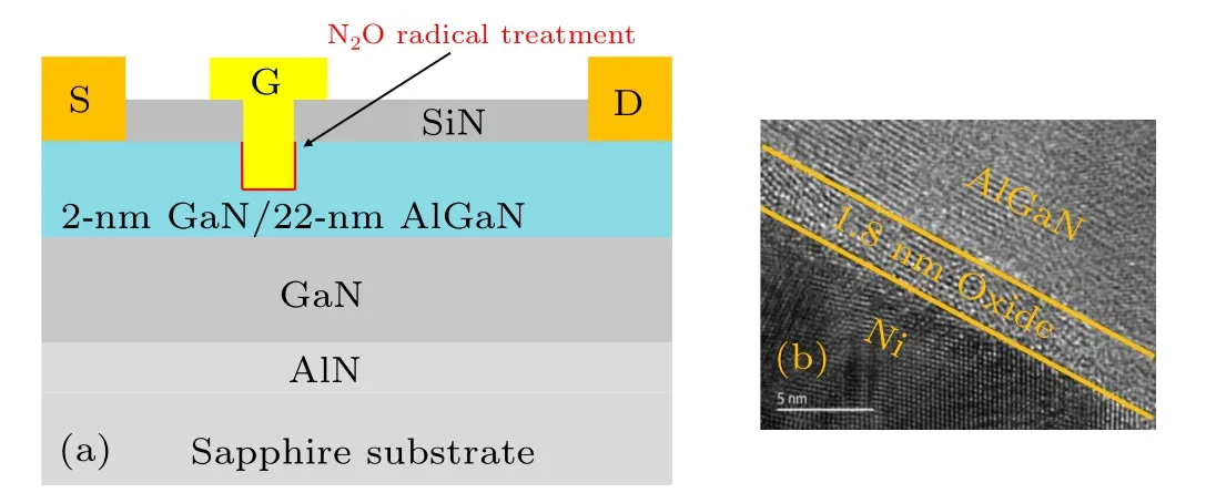
Fig. 1. (a) Schematic cross section of the proposed AlGaN/GaN HEMTs and(b)Scanning transmission electron microscopy image on a cross-section from the IST sample in the gate interface region.
The process flow started with a Ti/Al/Ni/Au ohmic contact deposited by electron beam evaporation, followed by annealing at 840°C for 30 s in nitrogen ambient.Then the device isolation was achieved by BCl3/Cl2based etching with the etching depth of 140 nm. The measured ohmic contact resistance was 0.42 Ω·mm using transmission line model (TLM).A 60-nm SiN passivation layer was deposited with PECVD,and the gate foot was defined by photolithography. After the SiN layer under the gate electron was removed by CF4-based plasma,gate recess was performed by BCl3/Cl2-based plasma with ICP, of which total etching depth is 74.5 nm by atomic force microscope (AFM). Two control groups were set. The sample A without IST process served as a control group after gate recess etching,and the sample B was treated by N2O radical to react with the AlGaN surface in high vacuum reaction chamber of ICP for 20 minutes. The ICP source power and the bias power were applied by 200 W and 0 W,respectively. The chamber pressure was 15 mTorr(1 Torr=1.33322×10²Pa)with the N2O flow rate of 60 sccm. And the temperature of chuck was 40°C. There was no DC-bias voltage in the entire IST process. In the gate region of sample B, a 1.8-nm oxide layer was obtained as shown in Fig. 1(b). An Ni/Au(45 nm/120 nm) gate metal was deposited by electron beam evaporation after gate head lithography. In the whole processes,the two samples have the same process conditions except the IST time. The two types of HEMTs have a gate width of 50 μm, gate–source spacing of 1.4 μm, gate length of 0.6 μm, and gate–drain spacing of 2.8 μm. In addition,a circular shape Schottky barrier diode (SBD) with an anode radius of 65.0 μm were used for the capacitance–voltage measurements.
3. Results and discussion
The surface morphology of two samples in gate region scanned by AFM is shown in the Fig. 2(a) (sample A) and 2(b)(sample B).After IST,the surface roughness in terms of root mean square(RMS)changes from 0.336 nm to 0.286 nm,which shows IST process does not deteriorate the surface morphology of AlGaN layer.
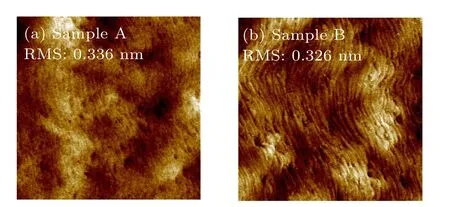
Fig. 2. The morphology of recess gate with (a) no IST (sample A) and (b)IST(sample B)by AFM scanning(5 μm×5 μm).
The transferI–Vand output characteristics of the two devices atVd=10 V are compared as illustrated in Figs. 3(a)and 3(b). Table 1 shows the threshold voltages (Vth), peak transconductance (Gmmax) andION/IOFFof the two kinds of HEMTs. TheVthis defined as the gate-bias intercept of the linear extrapolation of drain current at the peak transconductance.It is found that theVthof sample A is-1.6 V and that of sample B is-1.3 V which is floating forward by 0.3 V. This is because that the effective thickness of the barrier layer decreases due to the oxidation of 1.8-nm AlGaN on the surface of the barrier layer by IST (as shown in Fig. 1(b)).[21]AtVgof-6 V, the drain leakage currents for two types of HEMTs are 5.3×10⁻⁹and 1.7×10⁻⁷A/mm with and without IST respectively. The correspondingION/IOFFratio increases by more than one order of magnitude. Figure 3(b)compares the output characteristics of two types of HEMTs,at a gate voltage of-6 V~2 V and step of 1 V.It is found that the on-resistance of the devices are the same as 2.8 Ω·mm and 2.7 Ω·mm for samples A and B respectively. And the saturation output currents of two kind of HEMTs were 905 mA/mm and 875 mA/mm. After IST, the on-resistance decreases slightly.The on-resistance of HEMT can be expressed by the following expression:

whereRon-total is the total on-resistance,Rconis the ohmic contact resistance determined by transfer line method,Rgsis the channel resistance between gate and source,Rgdis the channel resistance between gate and drain,andRrecessrefers to the channel resistance under the gate.Judging from the TLM analysis, the contact resistance (Rcon) and block resistance (R□)for the HEMTs without IST are the same as the ones for the HEMTs with IST.Thus,Rcon,Rgs,andRgdremain unchanged during IST because of the constantRconandR□. And the variation ofRon-total depends onRrecess. This means that the gate resistance of the HEMTs does not degenerate after IST. Figure 3(c)shows the gate Schottky characteristics of the two devices. WhenVg=-10 V, the gate leakage current decreases from 1.8×10⁻⁷A/mm before IST to 2.4×10⁻⁹A/mm,which reduces by more than one order of magnitude. The Schottky barrier height can be extracted by the CV ring on the same sheet.[22]And the barrier height are 1.02 eV and 0.86 eV,respectively,for the HEMTs with IST and without IST.The increase of Schottky barrier height not only suppresses the gate reverse leakage current,[23,24]but also promotes the positive drift of device threshold voltage.[21]Figure 3(d) shows the curve of channel electron field effect mobility(μFE)with gate bias in the linear region. TheμFEof the all HEMTs channel was extracted by fat field-effect transistors (FATFETs) withLsg,Lg,Lgd, andWGof 3 μm, 50 μm, 3 μm, and 100 μm to reduce the influence of source and drain resistances. The peakμFEof HEMT with IST is 1409 cm2/V·s, however, ones of HEMT without IST is 1349 cm2/V·s. It was probably due to the fact that N2O radicals repaired the etching damage of gate region to a certain extent and reduced the surface trap density of states.[25]
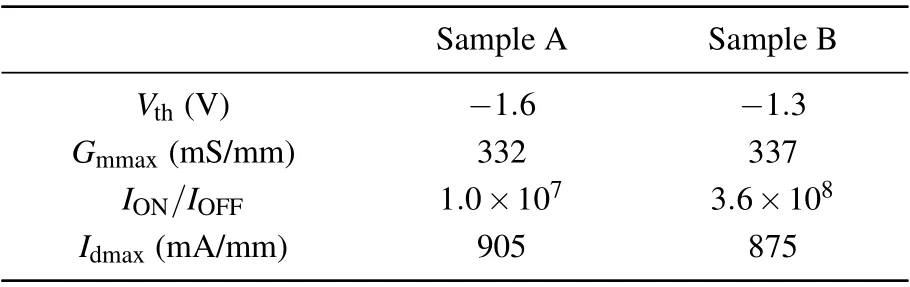
Table 1. Comparison of Vth,Gmmax,Ion/Ioff,and Idmax of HEMTs without and with IST.
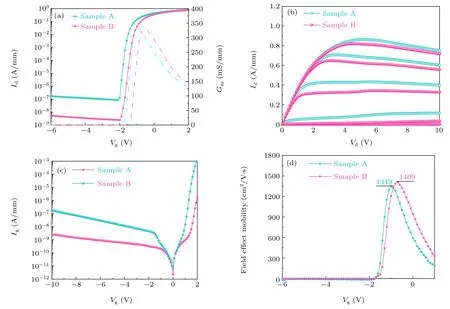
Fig.3. (a)Transfer characteristics,(b)output characteristics,(c)gate Schottky characteristics,and(d)μFE as a function of Vg for HEMTs with and without IST.
Figure 4 illustrates the capacitance–voltage characteristics of the two types of Schottky diodes with different treatment processes at 100 kHz. Compared with sample A, the turn-on voltage of sample B is floating by 0.3 V,which is consistent with the transfer characteristics shown in Fig.3(a).The depth profile calculated by theC–Vmeasurement shows that the peak concentrations of electrons for two samples are in the position of 9.5 nm,as shown in the inset of Fig.4. This shows that the chemical reaction between N2O radicals and AlGaN layer does not change the distance between gate electrode and two-dimensional electron gas(2DEG)channel. However,the 2DEG concentration(ns)of the channel after IST is reduced to 55%of that of the channel without IST,which may be because the IST process oxidizes the AlGaN surface layer and reduces the thickness of the remaining barrier layer.[26]The decrease ofnsleads to a slight decrease in the saturated output current of the device with IST, as shown in Fig. 3(b). What is more,the smaller thens, the more positive bias voltage is required to clamp off the channel, that is, the more positive the corresponding threshold voltage. Therefore,in this study,sample B(with IST)has a more positive threshold voltage.bonds are formed. Compared sample A, the significant enhancement of Al–O peak makes the core–level spectra of O 1s drift towards the Al–O peak with lower bond energy for sample B.These results are consistent with the corresponding spectral peaks of Al2O3prepared by physical vapor deposition method.[27]The IST process generates corresponding oxides,so as to improve the Schottky barrier height.[28,29]Therefore,the barrier height of the device with IST is higher than that of the device without IST.Moreover,it is found that the decrease of gate leakage current is related to the oxidation of the barrier layer,as figure 3(c)shows.
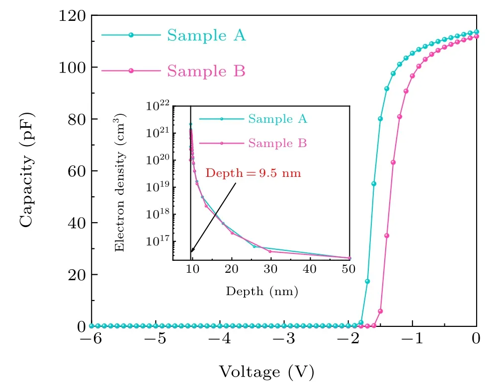
Fig.4. The C–V characteristics of sample A and sample B.
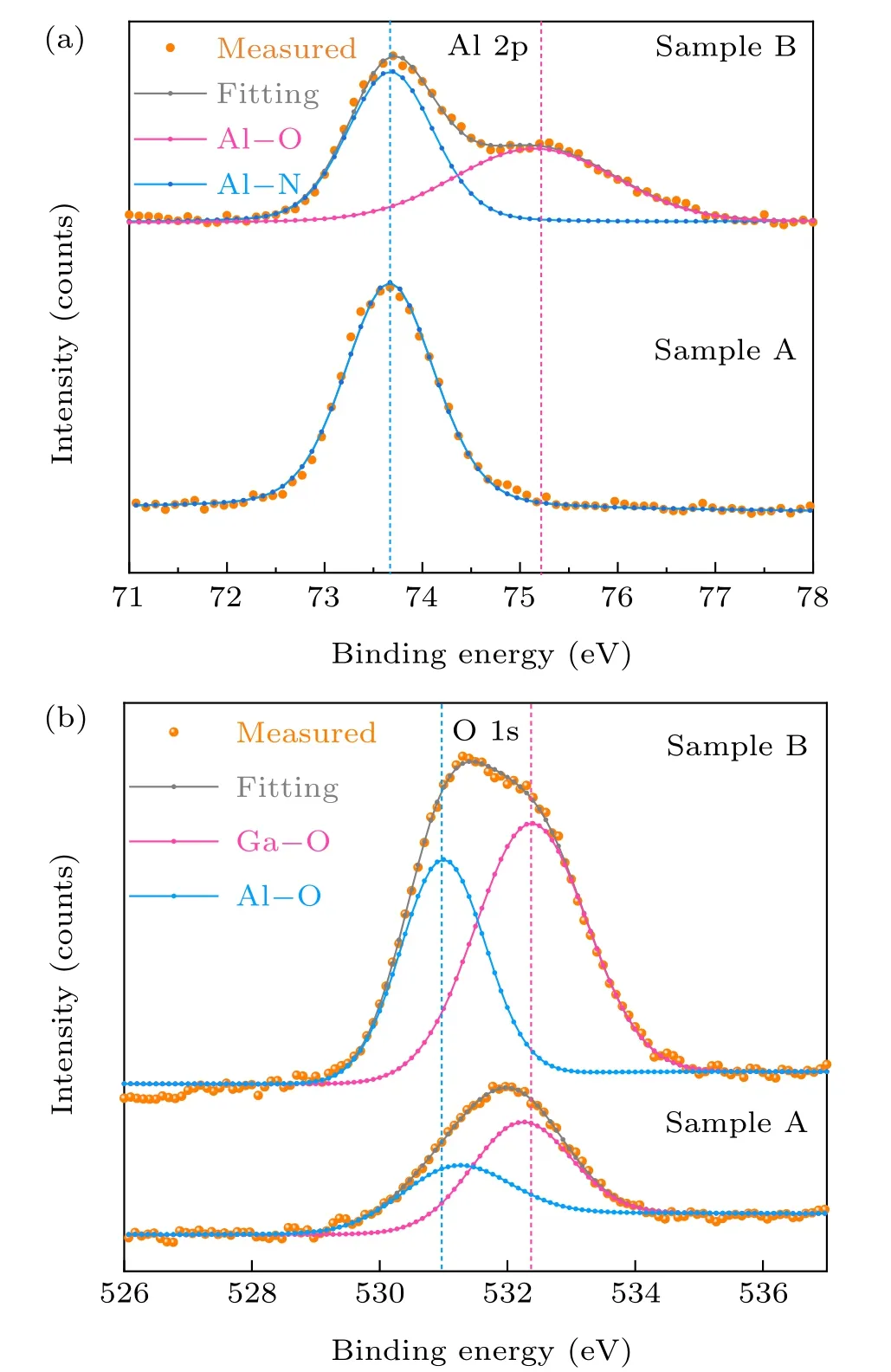
Fig.5. XPS spectra from(a)Al 2p and(b)O 1s core levels of AlGaN surface with and without IST.
The XPS method is also adopted to investigate the surface chemical composition of two samples. The Al 2p and the O 1s core level spectra are illustrated in Figs. 5(a) and 5(b),respectively. As shown in Fig.5(a),the Al 2p core–level spectrum is a coupling of two components corresponding to Al–O and Al–N bonds. After IST, the intensity of Al–O bond was elevated, indicating that some Al–N bonds on the surface are broken and meanwhile some Al–O bonds are formed. Figure 5(b) demonstrates that the O 1s core–level spectrum is a coupling of two components corresponding to the Al–O and the Ga–O bonds. After IST,both intensity of Al–O and Ga–O bonds were elevated as well,illustrating that Al–N and Ga–N bonds on the surface are broken while some Al–O and Ga–O
Figure 6 shows the pulse transfer characteristics of two types of HEMTs at a gate voltage of-6 V~2 V and the current collapse ratio can be expressed by the following expression:
where ΔIdsis the variation of pulse drain current atVg=2 V before and after electrical stress, andIds0is the pulse drain current atVg=2 V before applying electric stress.

Table 2. Comparison of pulse current collapse ratio of HEMTs with and without IST at(VGSQ,VDSQ=-4 V,0 V)and(VGSQ,VDSQ=-8 V,0 V).
As the Table 2 shows, sample A shows current collapse ratios of 1.9%and 4.9%at gate quiescent voltages of-4 V and-8 V,respectively. Sample B shows current collapse ratios of 0.4%and 1.8%.This indicates that IST has a certain inhibition effect on current collapse. What is more,the HEMTs without IST exhibited a forward floating ofVthby 0.18 V,while that for the ones with IST is only 0.06 V.The drift ofVthmay be due to the damage induced trap introduced in the process of recess gate etching,which has the ability to capture electrons.[30]
As demonstrated in Fig. 7, the current–gain cutoff frequencyfTand maximum oscillation frequencyfmaxof the two types of HEMTs were measured using network analyzer in a frequency ranging from 100 MHz to 40 GHz. The HEMTs with IST process deliver anfTof 22.4 GHz and anfmaxof 47.5 GHz(as shown in Fig.7(b)), resulting in a highfT×Lgof 13.4 GHz·μm. While the HEMTs without IST show anfTof 18.0 GHz and anfmaxof 38.8 GHz(as shown in Fig.7(a)).As shown in Fig.6,the IST process reduces the drift of threshold voltage, which shows its advantage in reducing the interface charge induced by trap. Because IST process could effectively reduce the interface charge,reduced the parasitic effect of the device,and then reduced the effective gate length of the device.[31]Therefore, the small signal characteristics of the device are improved.
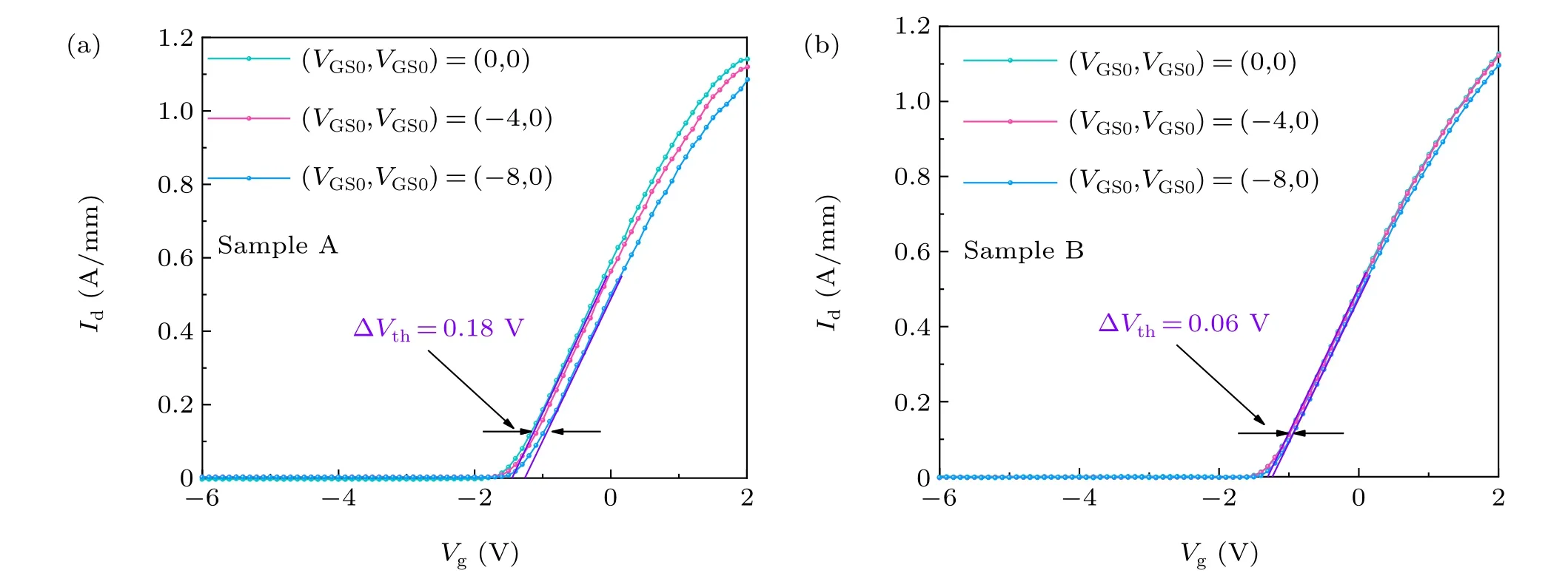
Fig.6.Pulsed I–V characteristics of HEMTs with(a)no IST and(b)IST at a drain voltage of 10 V for(VGSQ,VDSQ=0 V,0 V),(VGSQ,VDSQ=-4 V,0 V),and(VGSQ,VDSQ=-8 V,0 V).
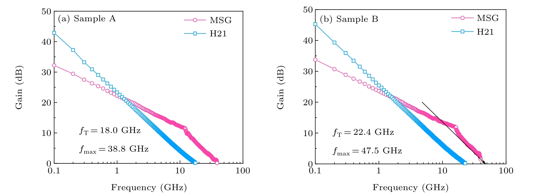
Fig.7. Small-signal characteristics of the fabricated HEMTs at VDS=10 V for the HEMTs(a)without and(b)with IST.
4. Conclusion
In conclusion,we proposed a method to reduce gate leakage of devices and investigated the effect of different processing time of IST on the surface of barrier layer under gate metal.The fabricated HEMTs with the IST process show a low reverse gate current of 10-9A/mm, high on/off current ratio of 3.6×10⁸, and highfT×Lgof 13.44 GHz·μm. Energy spectrum analysis of XPS shows the surface of AlGaN barrier layer is transformed into gallium oxide and alumina oxide,which proved by the cross-sectional TEM.These excellent results depict the great potential of the IST process applied for high frequency and high power operation. Especially, for RF devices with small gate length used in millimeter wave band,IST process can reduce the gate length extension of the device and significantly improve the high-frequency characteristics of the device and promote the development of RF devices.
Acknowledgments
Project supported by the National Key Research and Development Program of China(Grant No.2018YFB1802100),the National Natural Science Foundation of China (Grant Nos. 62104184, 62090014, 62104178, and 62104179), the Fundamental Research Funds for the Central Universities of China(Grant Nos.XJS201102,XJS211101,XJS211106,and ZDRC2002), and the Natural Science Foundation of Shaanxi Province, China (Grant Nos. 2020JM-191 and 2018HJCG-20).
猜你喜欢
杂志排行

Chinese Physics B的其它文章
- A nonlocal Boussinesq equation: Multiple-soliton solutions and symmetry analysis
- Correlation and trust mechanism-based rumor propagation model in complex social networks
- Gauss quadrature based finite temperature Lanczos method
- Experimental realization of quantum controlled teleportation of arbitrary two-qubit state via a five-qubit entangled state
- Self-error-rejecting multipartite entanglement purification for electron systems assisted by quantum-dot spins in optical microcavities
- Pseudospin symmetric solutions of the Dirac equation with the modified Rosen–Morse potential using Nikiforov–Uvarov method and supersymmetric quantum mechanics approach