Strain drived band aligment transition of the ferromagnetic VS2/C3N van der Waals heterostructure∗
2021-09-28JiminShang商继敏ShuaiQiao乔帅JingzhiFang房景治HongyuWen文宏玉andZhongmingWei魏钟鸣
Jimin Shang(商继敏)Shuai Qiao(乔帅)Jingzhi Fang(房景治)Hongyu Wen(文宏玉)and Zhongming Wei(魏钟鸣)
1School of Physics and Electronics Engineering,Zhengzhou University of Light Industry&Henan Key Laboratory of Magnetoelectronic Information Functional Materials,Zhengzhou University of Light Industry,Zhengzhou 450002,China
2State Key Laboratory of Superlattices and Microstructures,Institute of Semiconductors,Chinese Academy of Sciences&Center of Materials Science and Optoelectronics Engineering,University of Chinese Academy of Sciences,Beijing 100083,China
Keywords:two-dimensional ferromagnetic material,van der Waals heterostructure,band alignment,strain
1.Introduction
Two-dimensional(2D)materials have been regarded as prospective candidates on account of the outstanding properties.[1–4]However,single 2D material does not possess perfect properties for practical applications,such as the zero-band gap of graphene limiting its applications in optoelectronic devices.Accordance with prior research,constructing van der Waals(vdW)heterostructure is purposefully carried out together to obtain many new properties beyond single components.[5–8]Nevertheless,the existing vdW heterostructures with the intrinsic ferromagnetic(FM)properties are rare.To develop the application of vdW heterostructures in spintronics,as well as memory and storge devices,the explorations of magnetic properties in vdW heterostructures are essential.Due to majority 2D materials are nonmagnetic,many methods to induce magnetic ordering have focused on the doping,defect,application of electric fields,and surface functionalization.[9–12]However,the external modulation would lead to the complex correlation of the orbital and the lattice.Since the long-range magnetic order was observed in Cr2Ge2Te6and CrI3,[13,14]many novel phenomena and 2D magnetic materials have been reported.While the lacking of FM vdW heterostructures to date hinders the uses of 2D materials in spintronic devices.Therefore,it is highly desirable to explore new 2D magnetic vdW heterostructures to extend their multifunctional applications.
Recently,as a new member of 2D transition-metal dichalcogenides(TMDs)family,the atomically vanadium disulfde(VS2)monolayer is confirmed to have an intrinsic FM semiconducting property,[15,16]which could be a suitable candidate for constructing 2D magnetic vdW heterostructures.Xionget al.reported that the Mg(OH)2/VS2heterostructure possesses the FM properties with high Curie temperature.[17]Duet al.theoretically predicted that a halfmetal state with 100% spin-polarized currents could be obtained by applying an electronic field in MoS2(WS2)/VS2vdW heterostructures.[18]However,the previous reports on the 2D atomically thin vdW heterostructures based on VS2are rare.As the 2D FM heterostructures have great potential application of nanoelectronic and spintronic devices,more FM vdW heterostructures based on VS2with desired properties should be designed.As a typical CN compound,C3N monolayer has recently been fabricated with remarkable electronic and optoelectronic properties.[19,20]Due to a wide spectral responsive range,C3N has its potential utilization in photocatalysis and various applications.[21–23]The C3N monolayer also has many excellent properties similar to graphene,for instance the high carrier mobility and high thermal conductivity.[21,24,25]Thus,the C3N monolayer will be an outstanding candidate for applications in electronic devices due to its suitable band gap,that is very different from graphene.[26]Interestingly,from the previous theoretical results,there is a good lattice match between the 3×3 supercell of VS2and the 2×2 of C3N.Therefore,the VS2/C3N would be conveniently prepared in experiments.In addition,VS2/C3N would be a magnetic heterostructure with suitable band gap,and should enhance the performance in practical spintronic devices.
According to the above statement,in this work,we construct the VS2/C3N van der Waals heterostructures,and discuss the electronic and magnetic properties of the heterostructures.Our first-principles results show that VS2/C3N heterostructures exhibit FM semiconducting ground states with multiple band alignments.Particularly,the intrinsic type III alignment indicates that the VS2/C3N vdW heterostructure is quite favorable for tunneling and spintronic devices.While the type-II band alignment in the spin-up channel can naturally realize p doping in the heterostructure,and the band alignments also can be tuned by an external strain.Our result provides the multiple electronic and magnetic properties of the heterostructures,which will be very attractive to the potential applications of 2D FM semiconducting heterostructures in electronic and spintronic devices.
2.Methods
Our simulations are all carried out based on the spinpolarized density functional theory(DFT)by employing the Vienna ab initio simulation package(VASP)code.[27]The exchange–correlation functional is described using the generalized gradient approximation(GGA)within the Perdew–Burke–Ernzerhof(PBE)formula.[28]The projectoraugmented wave(PAW)method[29]is modeled for the core electrons.Moreover,to correct the correlation effects between the localized V-3d electrons,we adopt Dudarev’s approach with the on-site Coulomb energy U=2 eV and exchange parameter J=0.87 eV in the spin-polarized DFT+U calculations.[30]The values for V 3d electrons have been checked to yield reliable results in existing theoretical works.[31–33]We also consider the interactions of the VS2/C3N vdW heterostructure using the DFT-D2 method of Grimme.[34,35]The plane-wave basis energy cutoff is set to 500 eV.The geometry structures are fully relaxed until the Hellmann–Feynman atomic force on each atom is less than 0.01 eV/˚A,and the total energy convergence criterion for electronic iterations is chosen as 10−5eV.In addition,the Monkhorst–Pack method in the Brillouin zone is sampled by 13×13×1 for the geometry optimization of the system.A vacuum slab of 20˚A along the z-axis is sufficient to avoid the interaction between layers and their periodic images.
3.Results and discussion
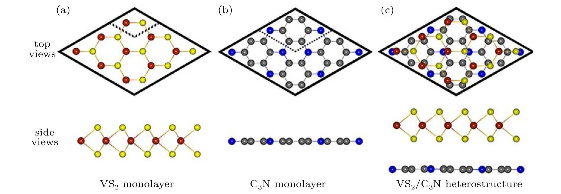
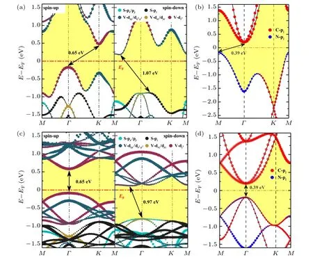
To construct the geometric model of the VS2/C3N heterostructures,we firstly discuss the structural parameters,electronic and magnetic properties of the VS2monolayer and C3N monolayer.Here we choose the most stable trigonal prismatic(2H)phase of VS2monolayer as shown in Fig.1.The honeycomb structure of 2H-VS2consists of two hexagonal atomic layers where the V atomic layer is sandwiched by the two S atomic layers.At the same time,C3N monolayer has the hexagonal graphene-like structure with one N atom surrounded by three C atoms,which can be regarded as a Ndoped graphene.Based on the minimization of the total energy,the optimized lattice parameter is 3.19˚A for VS2monolayer,meanwhile is 4.86˚A for monolayer C3N.Our results are in good agreement with the existing theoretical and experimental data.[17,18,36–38]In order to obtain the very small lattice mismatch,the 3×3 supercell of VS2monolayer and 2×2 supercell of C3N monolayer are proposed to form the VS2/C3N vdW heterostructures.The lattice mismatch is also calculated using the formulaΔ=2(a1−a2)/(a1+a2),where a1and a2are the lattice constants of the two isolated monolayers,respectively.Here the lattice mismatch is very tiny(~1.6%),which is beneficial for experimentally fabricating VS2/C3N vdW heterostructures.

Fig.1.(a)–(b)The top and side views of the VS2 and C3N monolayers.(c)Top and side views of VS2/C3N vdW heterostructure.The dashed rhombic frames represent the primitive cells,and the solid frame presents the 3×3 supercell of VS2 monolayer and 2×2 C3N monolayers,respectively.The red,yellow,blue,and grey balls represent the V,S,N,C atoms,respectively.

Fig.2.Orbital resolved band structures of monolayers(a)VS2 and(b)C3N calculated with unit cell,(c)VS2 calculated with 3×3 supercell,(d)C3N calculated with 2×2 supercell.The Fermi energy level is shifted to 0.0 eV and the sizes of symbols represent contributions from different orbitals.

By stacking the 3×3 supercell of VS2and 2×2 supercell of C3N vertically together,the VS2/C3N vdW heterostructure is constructed as shown in Fig.1(c).In our optimized heterostructure,the VS2and C3N still preserve their pristine geometric structures.The lattice parameter of the VS2/C3N vdW heterostructure is found to be 9.65˚A,between that of the VS2and C3N monolayers.Using the structural relaxation for the VS2/C3N heterostructure,the equilibrium interlayer distance is optimized to be~3.32˚A,which is defined as the vertical distance between the bottom S atomic layer in VS2and the C3N layer.In addition,when biaxial strain(in-plane)is applied,we still adopt the structural relaxation for each atom.From the results of the structural optimization,we find that the interlayer distance is unchanged with the applied in-plane strain.Thus,the interlayer distance remains unchanged in this paper.To further confirm the stability of the heterostructure,we also calculate the binding energy(Eb)using the formula

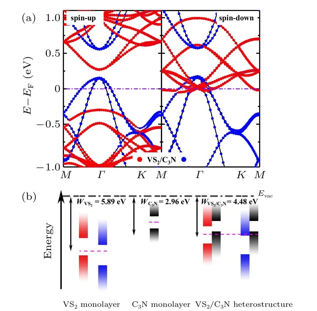
Next,we explore the electronic properties of the VS2/C3N heterostructure.Figure 3(a)shows the projected band structures of the VS2/C3N vdW heterostructure.A direct band gap is realized in the spin-up channel of the VS2/C3N heterostructure.The red and blue dots indicate contributions from the VS2and C3N layers,respectively.It can be seen that the stable FM properties are still kept in the VS2/C3N heterostructure,while the electronic structures in the spin-up and spin-down channels have an obvious modification comparison with those of the monolayers.The results indicate that the magnetic moment for the VS2/C3N vdW heterostructure is 0.9135µBand the magnetic moment of the heterostructure is slightly decreased compared with the magnetic moment of the unit cell(~0.9999µB)in the VS2monolayer.In the spinup channel,the CBM and VBM are contributed by the VS2and C3N layers,respectively,exhibiting a typical type-II band alignment.In addition,as shown in Fig.3(a),the Fermi level crosses the valence band,demonstrating a p-doping character in the C3N layer.The results indicate a charge(electron)transfer from the C3N layer to the VS2layer by composing VS2/C3N heterostructure,which can also be verified by comparing the work functions between the isolated VS2and C3N monolayers.The work functions of the C3N and VS2monolayers are 2.96 eV and 5.87 eV,which indicates that the highest Fermi level lies in C3N monolayer comparing with VS2monolayer both in the spin-up and spin-down channels.Thus,the electrons will flow from the C3N to the VS2monolayer,yet the holes transfer in the opposite direction until forming an equilibrium heterostructure.Therefore,the VS2/C3N vdW heterostructure displays an intrinsic type-II band alignment and p-doping characters in the spin-up channel,and the electrons and holes are respectively localized in the VS2and C3N layers,which is favorable for the practical optoelectronic devices.In comparison,a typical type-III band alignment is established in the spin-down channel,which indicates that the VS2/C3N vdW heterostructure is a broken gap vdW heterostructure with FM properties.As we know,the broken-gap heterostructures is suitable for the tunneling devices.Due to that there are considerable carrier migration in VS2/C3N heterostructures with no external electric field,it will result in an accumulation of electrons in the VS2layer and holes in C3N layer near the junction.Based on the separately accumulation of the carrier,a highly doped p+/n+heterojunction can be obtained in the VS2/C3N vdW heterostructure with no electrostatic or chemical doping.This special feature makes VS2/C3N heterostructure as an excellent material for negative differential resistance(NDR)devices.[38,42]
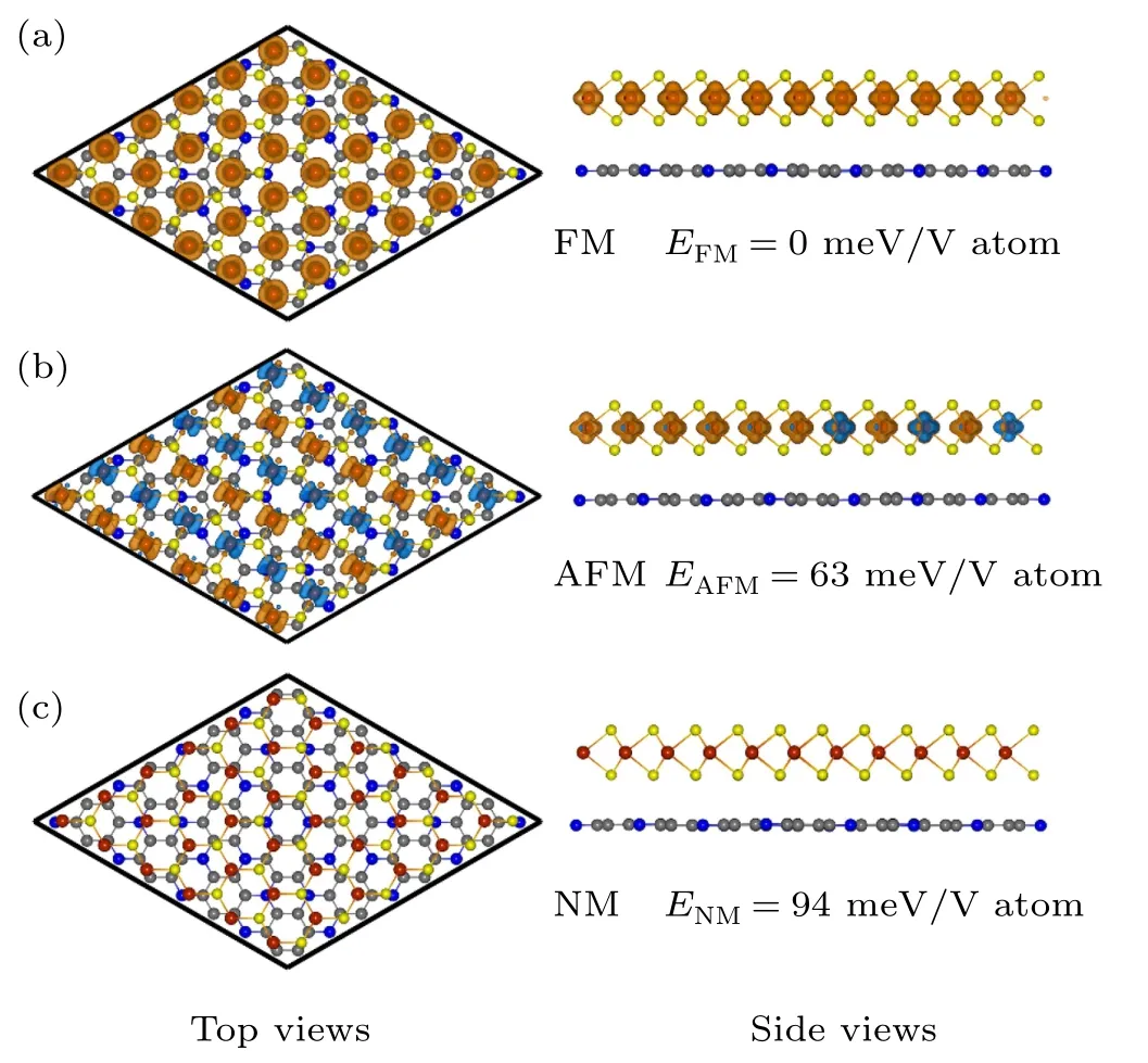
To discuss the magnetic properties of the VS2/C3N vdW heterostructure,the spin densities of the heterostructure are shown in Fig.4.We study the ground state magnetic properties of the heterostructure comparing all the possible magnetic orderings.The FM,non-magnetic(NM),and anti-ferromagnetic(AFM)are all calculated using a 2×2 supercell of the heterostructure,containing 36 V atoms.It can be seen that the magnetic moment of the heterostructure is mainly localized on the V atoms.The optimized configurations,local magnetic arrangements,magnetic moments,and energy are all shown in Fig.4 for NM,FM,and AFM states,respectively,with respect to the FM configuration(the energy of FM configuration is set to 0).Our numerical results indicate that the AFM ordering has the total energy of EAFM−EFM≈63 meV/V atom,and NM states has that of ENM−EFM≈94 meV/V atom,thus the FM ordering is found to be most stable compared with the AFM and NM ones.As a result,the VS2/C3N heterostructure presents the FM ground states,which indicates that the VS2/C3N heterostructure is a promising candidate for the application of the next-generation spintronic and optoelectronic devices.

Fig.3.(a)Projected band structure of VS2/C3N vdW heterostructure.The red and blue dots indicate contributions from VS2 and C3N monolayers,respectively.(b)Band alignment and work functions of VS2,C3N monolayers and VS2/C3N heterostructures.The Evac is referred to the vacuum level.

Fig.4.Spin densities of FM-,AFM1-,AFM2-,and NM-VS2/C3N heterostructure.The red and blue colors indicate the spin-up and spin-down sates,respectively.
It has been proved that strain engineering is an efficient method to modulate the electronic and transport properties in the practical 2D electronic devices,and the practical strain engineering is feasible to induce different compressive and tensile strains by bending the flexible substrate.[43]We also consider applying the strain to the VS2/C3N vdW heterostructure.To explore the strain effects on the electronic properties of the heterostructure,we apply the in-plane biaxial strains to VS2/C3N heterostructures.In this work,we just focus on the effect of the applied proper strains on their electronic properties,and the range of our considered strain can be easily achieved in the practical strain engineering.The biaxial strain is defined asε=(a−a0)/a0×100%,where a0(9.65˚A)is the lattice constant of the VS2/C3N vdW heterostructure in its equilibrium state,and a is the lattice constant of the strained VS2/C3N heterostructure.As shown in Figs.5(a)–5(c),it is clear that tensile strain is a more efficient to modulate the band alignment of the VS2/C3N vdW heterostructures both in the spin-up and spin-down channels.From the projected band structure of the heterostructure in Fig.5,the feature of the C3N layer is not apparent with the small tensile strain,but the VS2layer presents obvious effect under the same tensile strain.In the spin-up channel,the intrinsic type-II band alignment can be tuned into type-III band alignment when the tensile strain is 2%.Meanwhile,a doped p heterojunction is always hold.When the tensile strain reaches 4%,the heavy doped p+/n+heterojunction can be naturally realized in the spin-up channel.Based on the previous literature,[44]the 4%tensile strain will not induce the phase transition of the VS2monolayer.Comparing with Figs.5(a)and 5(c)in the spin-up channel,the CBM(consisted of VS2monolayer)in the spin-up channel moves down and crosses the Fermi level,thus the type-II band alignment is turned into type-III.On the other hand,in the spin-down channel the band alignment can also been modulated by the tensile strain.The intrinsic band alignment in the spin-down channel with no strain is type-III.However,when the tensile strain reaches to 4%,the CBM moves far from the Fermi level,and the type-II band alignment with p doping can be obtained in the spin-down channel.In addition,it can be seen from the projected band structure in Fig.5 that the characteristic of the p doping is always preserved with applying the tensile strain.Namely,the band alignments in the two spin channels can be effectively tuned by applying tensile strain,and an interchangement between the type-II and type-III band alignments can be realized.

Fig.5.Evolution of the projected band structures of VS2/C3N heterostructure with different in-plane biaxial strains.
4.Conclusion
We discuss the electric and FM properties of the VS2/C3N van der Waals heterostructure.The results present that stable ferromagnetic ordering and colorful electronic properties are established by constructing the VS2/C3N vdW heterostructure.Different from the monolayers,the VS2/C3N heterostructure presents a direct band gap with type-II band alignment and p-doping characters in the spin-up channel of the VS2/C3N heterostructure,which indicate that VS2/C3N FM heterostructures are fit for a high-efficiency optoelectronic application.On the other hand,a typical type-III band alignment with a broken-gap in the spin-down channel makes it a promising material for tunneling devices.Furthermore,the tuning properties can be induced by applying tensile strain.An interchangement between the type-II and type-III band alignments can be realized in the two spin channels with proper tensile strain.The attractive magnetic properties and the unique band alignments can provide multiple ways to utilize new FM heterostructures in future spintronic and optoelectronic devices.
杂志排行
Chinese Physics B的其它文章
- Multiple solutions and hysteresis in the flows driven by surface with antisymmetric velocity profile∗
- Magnetization relaxation of uniaxial anisotropic ferromagnetic particles with linear reaction dynamics driven by DC/AC magnetic field∗
- Influences of spin–orbit interaction on quantum speed limit and entanglement of spin qubits in coupled quantum dots
- Quantum multicast schemes of different quantum states via non-maximally entangled channels with multiparty involvement∗
- Magnetic and electronic properties of two-dimensional metal-organic frameworks TM3(C2NH)12*
- Preparation of a two-state mixture of ultracold fermionic atoms with balanced population subject to the unstable magnetic field∗
