面向新一代众核处理器的高性能SNC的设计与验证*
2021-09-15徐海文
徐海文 张 洋
(国防科技大学计算机学院 长沙 410073)
1 Introduction
Since the Stanford researcher proposed"Single-Chip Multi-Processors[1~2]",also known as"Multi-core Processors",in 1990s.Multi-core architecture has gradually become the mainstream of general purpose processors.It develops according to the Moore's law[3]and enters the so-called"multi-core era[4]".The number of cores in the processor is 32 or even hundreds of cores.At present,the mainstream structure of multi-core processors is the heterogeneous fusion structure of"generous-purpose DSP[5]core + application-specific core". The application-specific cores include isomorphic multi-core structures and heterogeneous multi-core structures.The number of cores in the isomorphic many-core structure is above 32 cores,and the inter-core interconnection uses an On-chip interconnect network.
As the number of cores increases,the complexity of the interconnection structure between the cores and the On-chip network will multiply,which will lead to a sharp increase in interconnect area.Thus will increase the long line delay and reduce the clock frequency.At present,super-node[6]structure is mainly used in processor design to solve this problem.Super node is composed of several cores,and data interaction between several cores and on-chip network[7]is realized by a super node controller(SNC).This structure will reduce the area of interconnect and avoid the impact of long-line delay.At the same time,it will reduce the complexity of processor design and verification.In this work,we design a high performance super node controller.The main innovations of my work are as follows.
1)Advanced eXtensible Interface(AXI)[8]compatible design;
2)Reduce on-chip network bandwidth pressure;
3)Reduce bandwidth pressure in core;
4)Friendly to programmer,it can tackle unaligned memory access[9],especially transfer mode,etc.
2 SNC Design
2.1 Overall Structure of SNC Based on AXI Bus
AXI bus protocol is a high-performance,high-bandwidth,low-latency on-chip bus which introduced by ARM.It is widely recognized and used throughout the semiconductor industry.The key features of AXI protocol are:
1)Separate address/control and data phases;
2)Support for unaligned data transfers using byte strobes;
3)Burst-based transactions with only start address issued;
4)Separate read and write data channels to enable low-cost Direct Memory Access(DMA)[10];
5)Ability to issue multiple outstanding addresses,etc.
These features allow the AXI bus to be applied at a higher clock frequency and provide higher data throughput at the same clock frequency.At the same time,the AXI bus has higher data bus bandwidth,and the chip design based on the AXI bus protocol has better flexibility and portability.
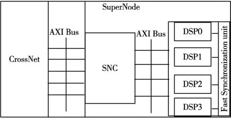
Fig.1 Schematic diagram of data interaction between DSP cores and on-chip network
The design of SNC is based on the AXI bus protocol.As shown in Fig 1,the super node consists of 4 DSP cores,a fast synchronization unit[11]and a SNC.The SNC is a relay control center for data interaction between 4 DSP cores and the On-chip network.It enables data storage,data arbitration,data transfer,data distribution,data unicast and broadcast[12]operations,etc.
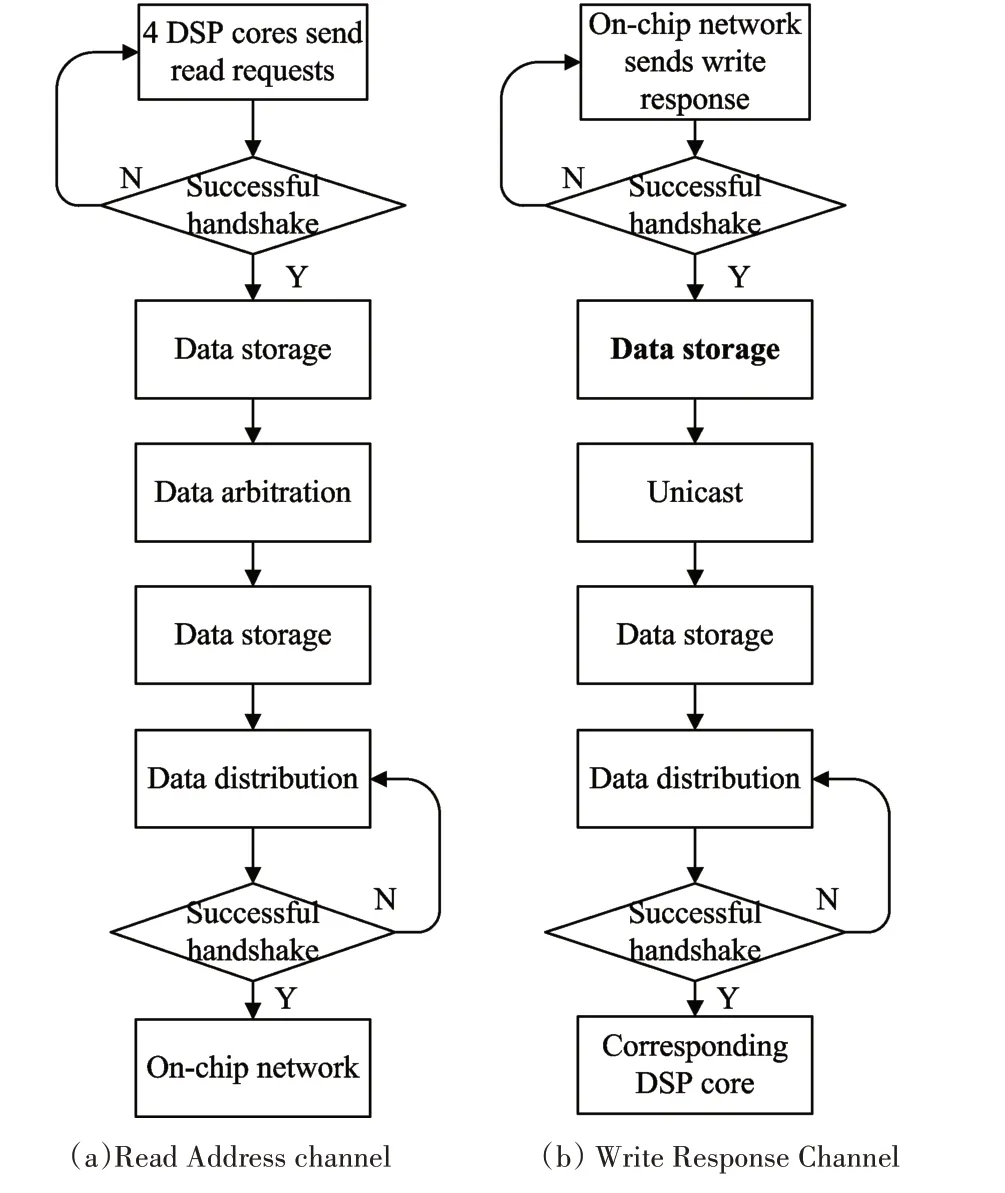
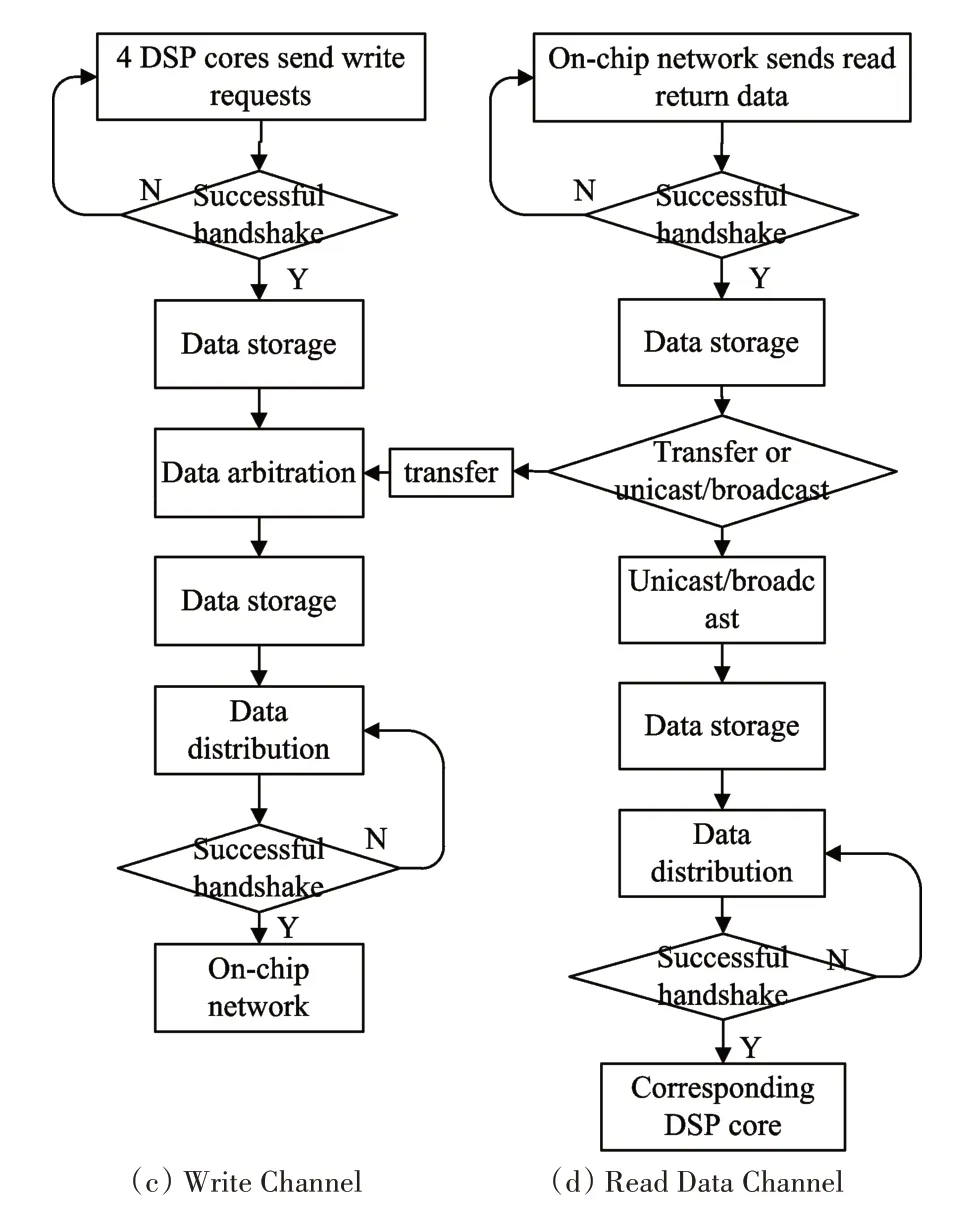
Fig.2 Four Data Channel in the SNC
As shown in Fig2,there are 4 data transmission channels in the SNC,which are the read address channel,the read data channel,the write channel and the write response channel.The write channel of the SNC is connected to the write address channel and the write data channel of the On-chip network,and the other three channels of the SNC are connected to the other three channels of the On-chip network.
Read Address Channel:As shown in Fig2(a),in the read address channel,4 DSP cores act as the master and are responsible for initiatively sending read requests to the SNC.Then the SNC packages,stores,arbitrates and distributes the data which sent by the 4 DSP cores,and sends the data to the On-chip network which acts as the slave.
Write Channel:As shown in Fig2(c),in the write channel,4 DSP cores act as the master and are responsible for initiatively sending write addresses and write data to the SNC.Then the SNC packages,stores,arbitrates(arbitration also includes reading data transferred by read data channels)and distributes the data which sent by the 4 DSP cores,and sends it to the On-chip network which acts as the slave.
Read Data Channel:As shown in Fig2(d),in the read data channel,the On-chip network acts as the master and the DSP cores act as the slave.If the read request is answered,the read return data will be packaged,stored,transferred,unicast,broadcast and other operations in the SNC,and then sent back to the corresponding DSP cores.
Write Response Channel:As shown in Fig2(b),in the write response channel,the On-chip network acts as the master and is responsible for initiatively sending write response data to the SNC.Then the SNC packages,stores,unicast and distributes data and sends it to the corresponding DSP core which acts as the slave.
2.2 Synchronous FIFO Design
In this article,SNC uses synchronous FIFO[12~13],a first-in and first-out data buffer,for data storage.The composition of synchronous FIFO has two parts which are the address control part and the data storage part.Synchronous FIFO can only write data sequentially and read data sequentially.And its data address is automatically added by internal read/write pointer.It is not possible to read or write a certain data by the address line like a normal memory.The synchronous FIFO has two address pointers,one for writing data to the next unread memory location and one for reading the next unread memory location.
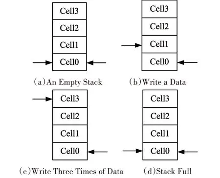
Fig.3 Synchronous FIFO Read and Write Process
The read and write process of the synchronous FIFO with depth 4 is shown in Fig3.When stack is empty,the read data pointer and write data pointer point to the first memory location.When writing a data,the write data pointer points to next memory location.After three write data operations,the write data pointer points to the last memory location.After four consecutive write operations,the write points will return to the first location and display the stack status is full.The data read operation is similar to the write operation.When reading a data,the read pointer will move to the next memory location until all data is read.At this point,the read pointer returns to the first location,and the stack status is empty.
2.3 Data Arbitrator Design
In this paper,SNC uses round-robin arbitration[14~15]for data arbitration,which is divided into two phases:the loop of priority signals and the loop of output.Using 2-bit PRI signal to control the priority of 4 channels in the 4-to-1 data arbitration.There are four channels,such as channel0,channel1,channel2 and channel3.The cyclic process of the PRI signal is shown in Fig4.When PRI=00,the priority of channel0 is the highest.And if the data of channel0 is valid,the data of channel0 is output first.Then the PRI signal is incremented to 01.After four consecutive operations,the PRI signal changes back to 00 and the cycle continues.When the priority is certain,such as PRI=00,the output loop is shown in Fig5.At this time,the output of the channel0 has the highest priority,and if the data of channel0 is valid,output this data.If it is invalid,continue to judge whether the data in channel1 is valid,and so on.
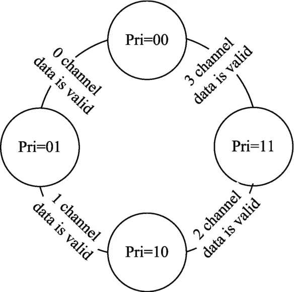
Fig.4 PRI Signal
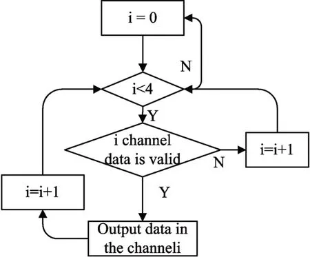
Fig.5 Output process at PRI=00
2.4 The Unicast and Broadcast Design
The unicast operation of the read data channel is to send the read return data to the corresponding DSP core according to the ID signal which returned by the On-chip network.The broadcast operation of the read data channel is to send the read return data to the corresponding DSP cores according to the 4-bit VECTOR signal which returned by the On-chip network.The priority of the VECTOR signal is higher than that of the ID signal.When the two signals are valid at the same time,the ID signal is ignored.When the VECTOR signal is invalid,ID signal is used as the judgment basis.The correspondence between the ID signal and the DSP core is shown in Table 1.
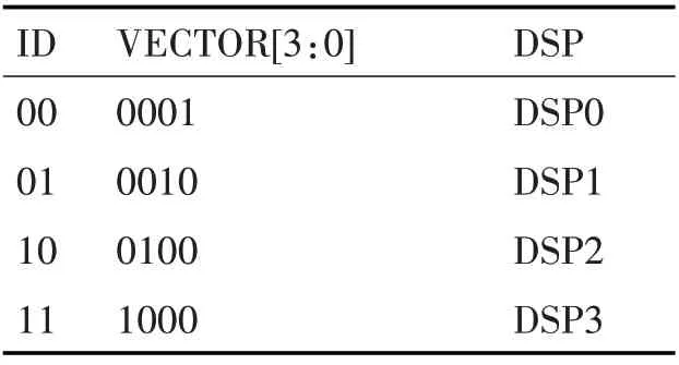
Table 1 Correspondence of ID,PRI,DSP Cores
In the SNC design,in order to simplify the complexity of the design of the read data channel,the data unicast and the data broadcast are combined into one data transmission mode.It is divided into two parts,which are the conversion phase and the transmission phase.The conversion phase is to convert the ID signal to the VECTOR signal during data unicast.The correspondence is shown in the Table1.The transmission phase is to broadcast data.

Table 2 SNC Synthesis Performance Indicators
The specific process of broadcasting is shown in Fig6.When the data is broadcast,the broadcast data is copied to data0,data1,data2,data3.Then determine the number of DSP cores that need to be broadcast according to the VECTOR signal.For the DSP core that is not being broadcast,the corresponding Count signal is set high.For the DSP core that needs to be broadcast,it is necessary to judge whether the DSP core has received the data.If the DSP core has received data,the corresponding Count signal is set high.If the DSP core has not received data,the loop continues.When Count0,Count1,Count2,Count3 are set high,the broadcast is completed,and then the next data is broadcast or unicast.
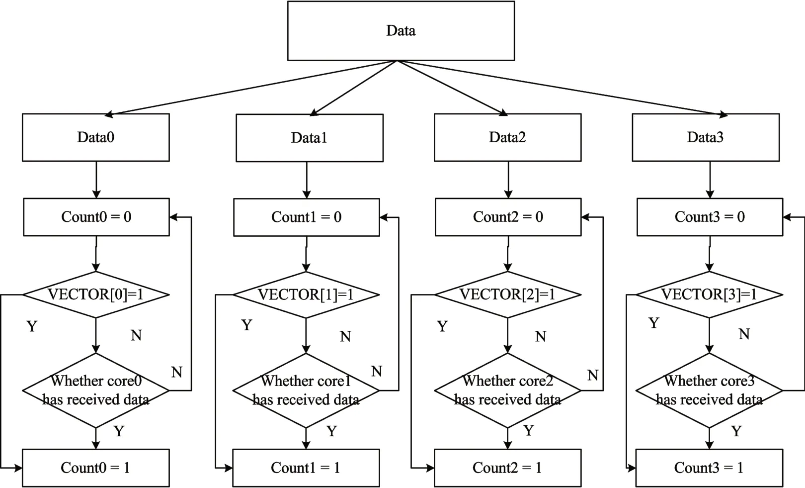
Fig.6 Transmission Phase
2.5 Data Transfer Unit Design
As shown in the Fig7(a),in the previous SNC design,when the DMA moves data from outside the DSP core to outside the DSP core,the SNC is only a data transmission channel,and the moving data process of the DMA is divided into three phases,which are the DMA sends a request to the storage 1,the DMA receives the read return data,and the DMA transfers the read return data to storage 2.
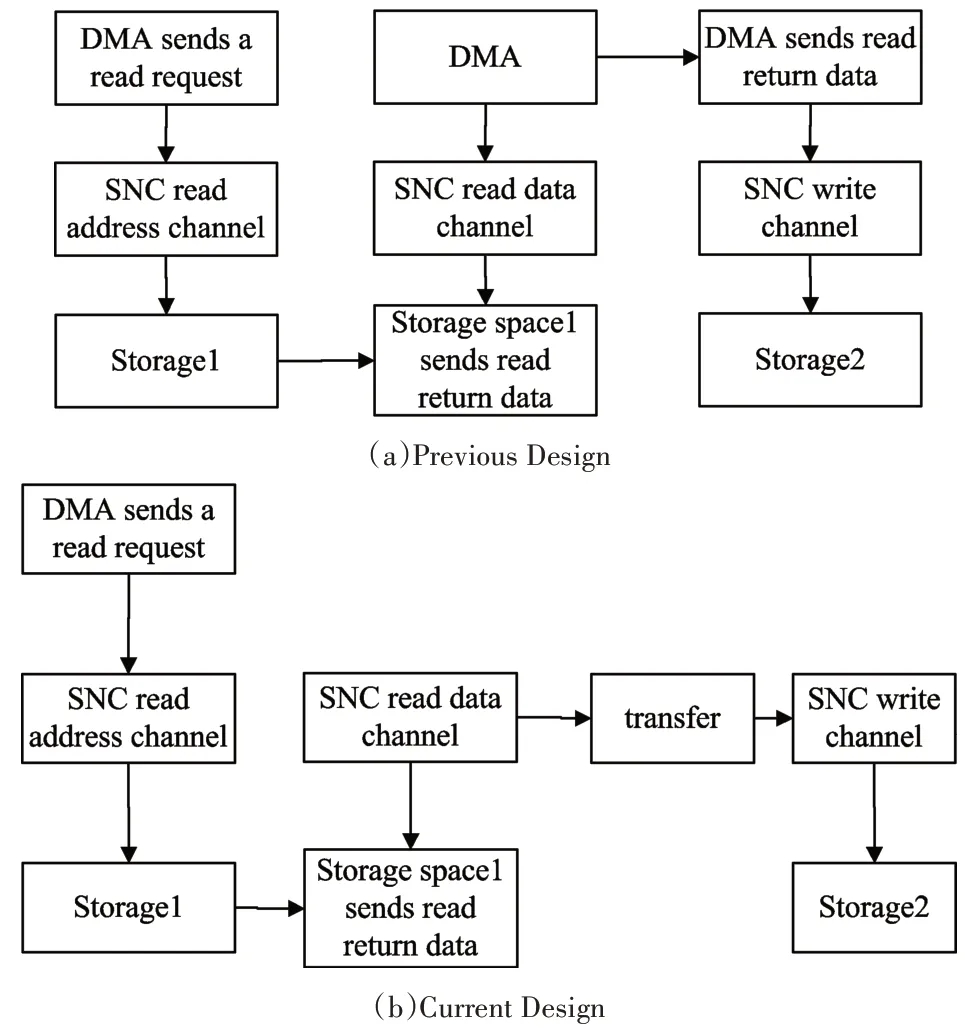
Fig.7 DMA Data transfer Processfrom outside of core to outside of core
As shown in the Fig7(b),in order to alleviate the bandwidth pressure of the DSP core when DMA moves data,we have added a Transfer mode to the SNC design.In this way,the data returned from the storage will not be sent to the DSP core.The transfer mode will reduce the data bandwidth pressure of the DSP core and reduce the data transmission path when the DMA moving data from outside the DSP core to outside the DSP core.
There may be cases when the read return address does not meet the address alignment requirement of the storage apace during the transfer process.Therefore,some data operations need to be performed on the read return data,such as data alignment and mask processing.The specific process of transfer is as follow:First,we need to know whether the return address meets the address alignment requirement of the storage.Output read return data if it matches.Process the read return data according to the address alignment requirements if it not matches.After data processing,the read return data is converted into two data,such as data0 and data1.Then judge whether the two data is valid by the mask signal in the data.Output the data if it is valid,and discard the data if it is invalid.
3 Conclusion
3.1 Verification
This article uses Cadence's NC-verilog for register transfer level verification of SNC.The SNC's verification platform[16]is shown in Fig8.It consists of 6 modules such as DUT,Gold Model,Interface,Top and Compare.The SNC's functional verification is mainly to compare the outputs of the DUT and the Gold Model by continuously sending incentives to the DUT and the Gold Model to verify that the function of the SNC is correct.After successful functional verification,we use Design Compiler of Synopsys to perform logical synthesis on SNC.The synthesis results are shown in table 2,SNC's critical path delay is 0.36ns.The area of the SNC is 39384.46um2.The total power of the SNC is 249.19mW.The verification and synthesis results show that the SNC has the correct function,and the main frequency can reach 2.0GHz,which meets the design requirements.
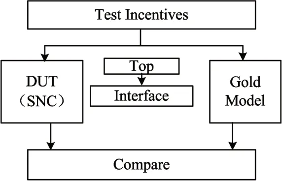
Fig.8 Functional Verification Platform
3.2 Conclusion
In summary,we design a SNC for high performance,high bandwidth,low latency multi-core processors design.Compared with the previous super node controller,this SNC not only implements the functions of the super node controller,but also adds some innovations.The innovations are as follows:
The SNC is compatible with AXI bus protocol,so it has greater flexibility and portability.
We have added a broadcast unit to the design of the SNC,so it can reduce on-chip network bandwidth pressure.
We have added a transfer unit to the design of the SNC,so it can reduce bandwidth pressure in core.
Friendly to programmer,it can tackle unaligned memory access,especially transfer mode,etc.