Time-varying coupling-induced logical stochastic resonance in a periodically driven coupled bistable system∗
2021-06-26YuangenYao姚元根
Yuangen Yao(姚元根)
Department of Physics,College of Science,Huazhong Agricultural University,Wuhan 430070,China
Keywords: logical stochastic resonance,coupled bistable system,time-varying coupling,Wiener process
1. Introduction
It is increasingly difficult to suppress noise as logic devices continue to shrink in size. The presence of the noise has increased the instability of logic devices and seriously limit the computing speed of computation devices based logic gates.[1]More recently, more and more efforts have focused on obtaining reliable logic operations. Inspired by stochastic resonance(SR),[2–7]Muraliet al. firstly put forward logical stochastic resonance (LSR), which characterizes that the reliability of logic gates can be realized in a proper window of noise intensity.[8]LSR has been successfully realized in electronic circuits,[9]optical systems,[10]synthetic genetic networks,[11–13]etc. As a potential mechanism for designing new-style logic gates,which can robustly work in noisy environment,LSR attracts more attention.
Besides the various types of noises,[14,15]other non-stochastic factors can also induce LSR-like phenomenon.[16–21]For example, Gupta and coworkers demonstrated that a bistable system subjected only to completely regular periodic forcing, despite having no stochastic influence, can also produce LSR-like phenomenon, and thus they termed this phenomenon noise-free LSR.[22]Furthermore, the constructive interplay of noise and periodic force can let systems adapt to varying noise level,and thus let systems can robustly operate in high noise conditions. This phenomenon is known as enhanced LSR.[23]In the real computational devices, such as integrated circuits, many logic gates are packed with wires into the surface of semi-conductor material to execute complex computation. Thus,coupling between different logic gates is a significant factor in designing computational devices.[24]Aravindet al. went beyond a single bistable system, and realized LSR in a coupled system.They termed this phenomenon coupling induced LSR. More specifically,when noise and coupling intensity are in optimal windows, the output of the coupled system can be mapped consistently to specific logic gate operations.[25]
However,the coupling intensity between two subsystems is assumed to be constant in the aforementioned study. Further,it has been demonstrated recently that time-periodic coupling intensity has significant influence on the dynamics of nonlinear systems.[26,27]Therefore, constant coupling is extended to time-varying coupling, and then investigate the effect of time-varying coupling on the reliability and response speed of logic operations in a periodically driven coupled bistable system via two measurement indexes: success probability and mean switching time.
2. Model and scheme
Consider a periodically driven coupled bistable system which consists of two bistable sub-systems coupled linearly and bi-directionally:[25]
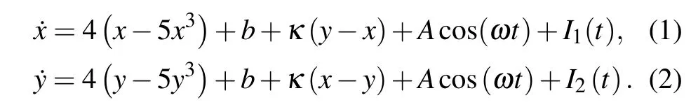
Here the bias parameterbcontrols the symmetry of double potential wells(Fig.1),and it takes value−0.28 for AND logic gate, and 0.28 for OR logic gate, respectively.[25]Acos(ωt)denotes periodic force. Without loss of generality, the amplitudeAand angular frequencyωare 0.5 and 10−0.5respectively, so that in the case of weak coupling intensity, reliable logic output cannot be obtained under periodic force driving.
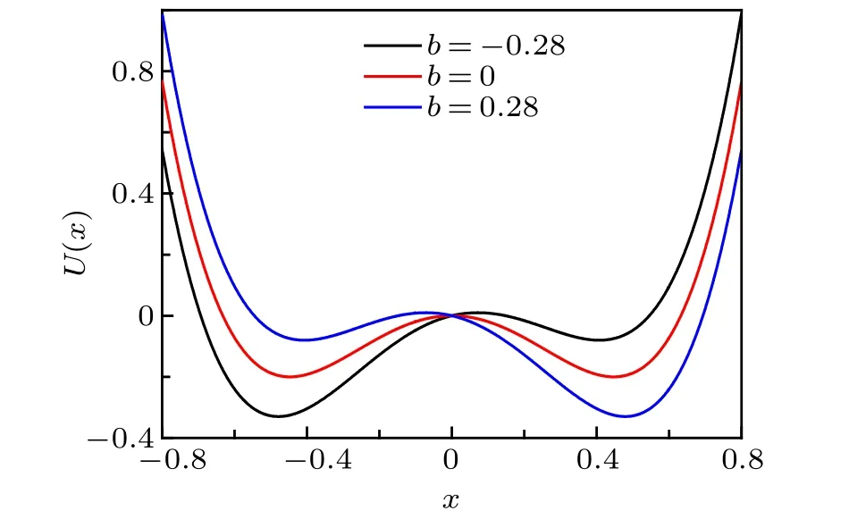
Fig. 1. Potential U(x)=5x4 −2x2+bx, which is obtained by integrating F(x)=4+b.
Fig. 2. The sampled time series of coupling intensity κ =c[1+sin(Nωt+σW(t))]W(t) is a standard Wiener process. Parameter σ stands for the intensity of the unit Wiener process W(t),which governs the degree of deviation of coupling intensity oscillation from the perfect periodicity. From top to bottom,σ =0,0.05,0.5,1,1.5. Larger σ means that coupling intensity oscillates more stochastically. N=1,c=3,and ω=10−0.5.

TheI1(t) andI2(t) are two independent randomly switched 2-level square wave input signals (From top to bottom, panels 1 and 2 in Fig. 3). Without loss of generality,I1andI2take value 0.8 when logic input is 1, and−0.8 when logic input is 0. Logic output of system depends on the state of system. Logic output is 1 ifxoryis greater than 0 (system lies in the positive well),or else logic output is 0(system lies in the negative well) (Fig. 1). Therefore, logic gate can be defined according to logical input–output association (Table 1). In order to measure the reliability of a specific logic operation,a success probabilityPof getting the desired logic output is defined as the ratio of the number of successful runs to the total number of runs.[21]A successful run means that for all possible logic input sets(Table 1),each output of system matches the desired logic operation at each time step,allowing to exclude small transience. The small transience is defined as the 10%of each time interval.[14,30]The total number of runsRis 100 in our simulations. Note that increasing total number of runs does not lead to obvious differences in the results.In addition, mean switching time is obtained by averaging at least 500 switching time which the system takes averagely to switch from high to low states orvice versaafter the switching of input signal. Note that increasing total number of switching time does not lead to obvious differences in the results. Mean switching time is used here to characterize the response speed of logic devices. In order to evaluate the degree of synchronization between two subsystems, a synchronization factorδis defined as follows:
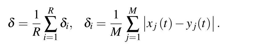
HereMis set to 4×10⁶. Clearly,lessδindicates better synchronization.
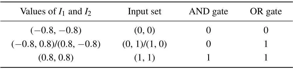
Table 1. Truth table for logic AND&OR gates.
3. Results
When the frequency of coupling intensity is less than that of periodic force, such as log10(N)=−1 (from top to bottom, panels 3 and 4 in Fig. 3), the state (xory) cannot be consistently mapped to AND or OR logic output according to logical input–output association (Table 1). Thus, the system cannot work robustly as a given logic AND or OR gate.However, when coupling intensity oscillates regularly with relatively high frequency than that of periodic force, such as log10(N)=1 (from top to bottom, panels 5 and 6 in Fig. 3),the state (xory) can be consistently mapped to AND or OR logic output according to logical input–output association(Table 1). Consequently, the system can robustly operate as a specific logic gate. Furthermore,it is easy to switch from one logic gate to another by changing the biasb(b=−0.28 for logic AND gate,b=0.28 for logic OR gate),so the logic gate is flexible(Fig.3). It is noteworthy that for the AND and OR logic operations,the qualitative results are very similar,due to synchronization between two subsystems,so onlyxis used to obtain a logic output in the following sections.
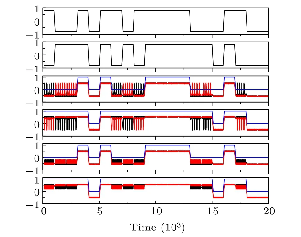
Fig.3. The sampled time series of input signals I1 and I2,x(black),y(red),and logic output (blue) of logic AND or OR gate. From top to bottom,panels 1 and 2 indicate the randomly switched streams of input signals I1 and I2, panels 3 and 4 cannot yield consistent AND & OR logic outputs(log10(N)=−1), while panels 5 and 6 can yield consistent AND & OR logic outputs(log10(N)=1). c=3,and σ =0.
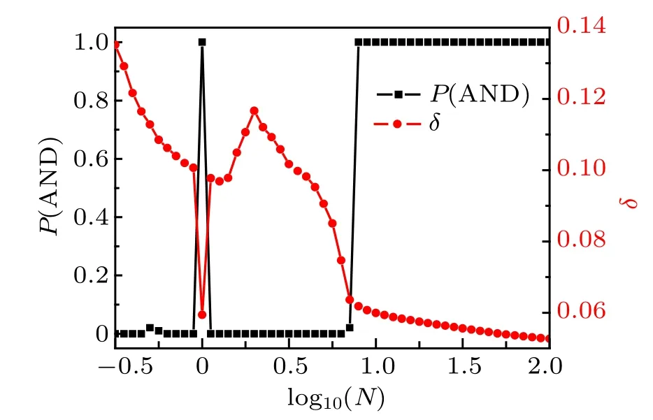
Fig. 4. The dependences of success probability P(AND) and synchronization factor δ on increasing log10(N)for logic AND gate. c=3,and σ =0.
A quantitative measure of success probabilityP, which depicts how reliably this system performs as a logic device,can be used to further confirm the above observed results.P=1 means that a reliable logic output is always available for each random stream of input signal(I(t)=I1(t)+I2(t)).As shown in Fig. 4, it is very obvious as the frequency of coupling intensity increases, one can observe a very sharp transition fromP ≈0 toP= 1 in the curve ofP versuslog10(N) (Fig. 4), which indicates the occurrence of timevarying coupling-induced LSR. Interestingly, when the frequency of periodic coupling intensity is precisely equal to that of periodic force (i.e.log10(N)=0), one can always obtain reliable logic operation (P=1), but it is not robust and tiny frequency difference between coupling and periodic force will seriously destroy the reliability of logic operation (Fig. 4).Consequently, coupling intensity with high frequency ratio is an optimal option to obtain a reliable and robust logic operation. In addition, a synchronization factorδis introduced to describe the degree of synchronization between two subsystems. It is quite clear that worse synchronization denoted by largerδcan account for why reliable logic operation cannot be obtained when log10(N)<0.9(Fig.4).

Fig.5. Contour plots of success probability P(AND)(a)and mean switching time(b)in the c–log10(N)plane. The red shaded region in(a)indicates where the success probability P(AND) takes maximum value of 1. Therefore, it shows the occurrence of time-periodic coupling-induced LSR phenomenon. c=3,and σ =0.
Furthermore, contour plot of success probabilityP(Fig. 5(a)) is used to illustrate the global dependences of success probabilityPon both amplitudecand the ratio of frequency log10(N). As indicated by red shaded area where the success probabilityPtakes the maximum value of 1 (Fig. 5(a)), time-varying coupling induced LSR can be achieved in a relatively wide range of the frequency ratio. In addition, mean switching time is used to characterize the response speed of the system to the change of input signal. In the premise of obtaining reliable logic outputs, the effect of varying frequency ratio on mean switching time is investigated by virtue of contour plot(Fig.5(b)). For a given amplitudecor frequency ratio log10(N)of coupling intensity,smaller frequency ratio log10(N)or smaller amplitudectends to reduce mean switching time(Fig.5(b)), and thus results in faster response of logic devices.
Fig. 6. The dependence of success probability P(AND) on increasing log10(N) for various different σ (panel (a)). The dependences of success probability P(AND) and mean switching time on increasing σ for log10(N)=1.25 (panel (b)). The insert in Fig. 6(b) indicates the dependences of success probability P(AND) on increasing σ for log10(N)=0.Here c takes value 3.
In the examples above, coupling intensity oscillates periodically with time. In the following section, the effect of phase disturbance in the coupling intensity on the reliability and response speed of logic devices is investigated. Phase disturbance in coupling intensity is modeled by Wiener processW(t)with the intensityσ. Largerσmeans that more stochastically coupling intensity alters with time. For a given amplitudec=3,the dependence of success probabilityP(AND)on increasing log10(N)for differentσclearly show that largerσmakes the optimal window(whereP=1)of frequency ratio log10(N) become narrower (Fig. 6(a)). In order to illustrate this conclusion more clearly,for a given amplitudec=3 and a specific frequency ratio log10(N)=1.25, the curves of success probabilityP(AND)and mean switching timeversusincreasingσare drawn (Fig. 6(b)). It is evident that success probabilityP(AND) decreases rapidly if increasingσis over a certain threshold, such as 0.9 (Fig. 6(b)). Note that when the frequency of coupling intensity is equal precisely to the frequency of periodic force, tiny phase disturbance may drastically destroy the reliability of logic operations as shown in the insert (Fig. 6(b)), thus logic gate is not robust against phase disturbance. In order to show the effect of phase disturbance degreeσfrom a global perspective,the boundary lines between reliable region (i.e.region above the curve) (whereP=1)and unreliable region(whereP <1)are plotted in thec–log10(N) plane for differentσ(Fig. 7). Clearly, with the increase ofσ,the area of reliable region decreases drastically.
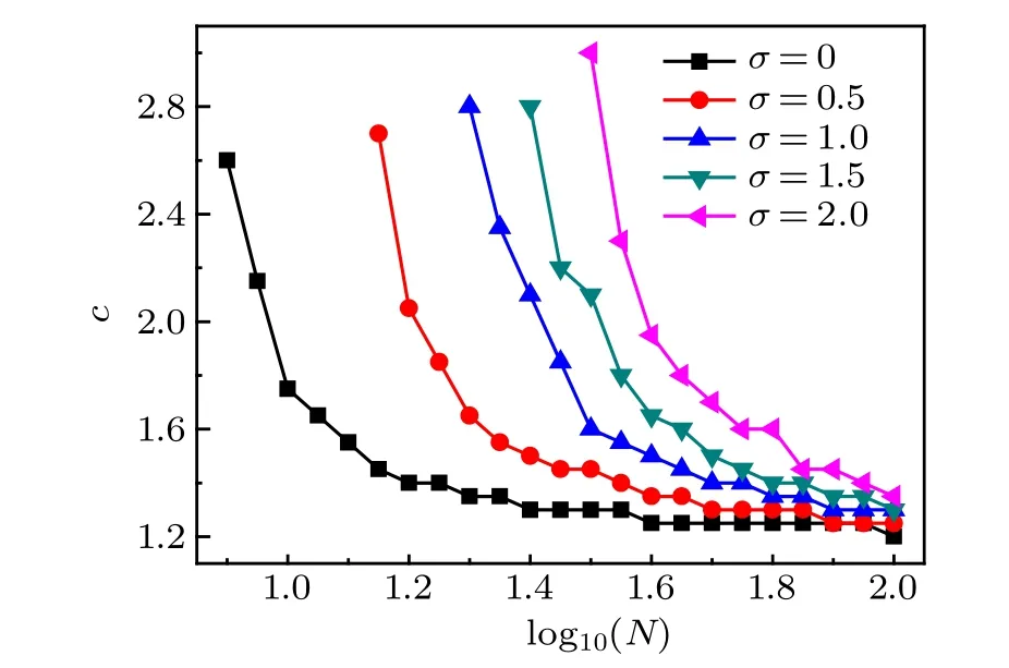
Fig.7. Effect of phase disturbance degree σ on the area of reliable region.The region above the curve indicates reliable region (where P=1). Obviously,with the increase of σ,the area of reliable region decreases drastically.
4. Conclusions
In summary,the effect of time-varying coupling intensity on reliable logic operation has been explicitly shown based on a coupled bistable system. It is possible to obtain a reliable logic operation in a periodically driven coupled bistable system with time-varying coupling intensity. In this study,two cases are considered: coupling intensity changes periodically or aperiodically with time. In the case of time-periodic coupling intensity,if coupling intensity oscillates periodically with relatively high frequency or the same frequency with periodic force,the system successfully yields the desired logical output. In the premise of obtaining reliable logic outputs,coupling intensity with smaller frequency ratio or smaller amplitudectends to reduce mean switching time, and thus results in faster response of logic devices. In the case of time-varying coupling intensity with phase disturbance, large phase disturbance reduces the area of reliable parameter region of coupling intensity and response speed of logic devices. Although the system behaves as a desired logic gate when the frequency of time-periodic coupling intensity is precisely equal to that of periodic force,the desired logic gate is not robust against tiny frequency difference between periodic force and coupling intensity,and slight phase disturbance in coupling intensity.As a consequence,periodic coupling intensity with high frequency ratio is an optimal option to obtain a reliable and robust logic operation in a periodically driven coupled bistable system in the presence of time-varying coupling intensity.
杂志排行

Chinese Physics B的其它文章
- Quantum computation and simulation with vibrational modes of trapped ions
- ℋ∞state estimation for Markov jump neural networks with transition probabilities subject to the persistent dwell-time switching rule∗
- Effect of symmetrical frequency chirp on pair production∗
- Entanglement properties of GHZ and W superposition state and its decayed states∗
- Lie transformation on shortcut to adiabaticity in parametric driving quantum systems∗
- Controlled quantum teleportation of an unknown single-qutrit state in noisy channels with memory∗