Effect of plasma step gradient modification on surface electrical properties of epoxy resin
2021-06-21JiyuanYAN闫纪源GuishuLIANG梁贵书HongliangLIAN廉洪亮YanzeSONG宋岩泽ChengkaiPENG彭程凯YuchanKANG康玉婵andQingXIE谢庆
Jiyuan YAN(闫纪源),Guishu LIANG(梁贵书),Hongliang LIAN(廉洪亮),Yanze SONG(宋岩泽),Chengkai PENG(彭程凯),Yuchan KANG(康玉婵) and Qing XIE(谢庆),∗
1 State Key Laboratory of Alternate Electrical Power System with Renewable Energy Sources,North China Electric Power University,Beijing 102206,People’s Republic of China
2 School of Electrical and Electronic Engineering,North China Electric Power University,Baoding 071003,People’s Republic of China
Abstract In this paper,plasma fluorination is combined with plasma silicon deposition to achieve step gradient modification on an epoxy resin surface.The physicochemical characteristics of samples are investigated and the electrical performances measured.The obtained results show that compared with untreated and single treated samples,the samples treated by step gradient modification significantly improve the flashover performance.According to experiment and simulation,the mechanism explanations are summarized as follows.First,it is found that the step gradient conductivity can effectively optimize the electric field distribution of a needle-needle electrode.Then,step gradient modification suppresses the accumulation of surface charge at the triple junction and makes the charge distribution more uniform.Furthermore,it can accelerate the surface dissipation on a high electrical field region and control the dissipation rate on a low electrical field region.All these results can restrain surface discharge and increase the flashover voltage.The step gradient modification method proposed in this paper provides a new idea for improving the surface insulation performance.
Keywords:plasma,epoxy resin,step gradient modification,flashover voltage,surface charge
1.Introduction
Gas insulated transmission line(GIL)is widely used because of its large transmission capacity,good operation stability,low capacitance load and is less affected by the geographical environment[1–3].As important components of GIL,insulators suffer from undetermined surface flashover events due to surface charge accumulation,which seriously impairs the insulation performance and threatens the safe and stable operation of electrical equipment[4–6].Li et al[7–9]comprehensively studied the relation between surface charge and surface flashover and proposed a series of methods to inhibit surface charge accumulation.Previous studies have shown that the surface flashover voltage can be significantly increased and the risk of insulation failure can be reduced by modifying the surface of insulators[10–12].As an effective approach to tailor the surface properties without affecting the material’s internal structures,plasma surface modification has become a favorable research method among researchers in recent years.In addition,it is also a reliable method to improve the surface flashover voltage of the insulators[13–15].
Currently,plasma fluorination and plasma silicon plating are the main methods of plasma surface modification on insulating materials.Due to the strong electronegativity of fluorine,many scholars have carried out in-depth research on plasma fluorination.Chen et al[16]utilized atmosphere pressure plasma jet(APPJ)to modify the epoxy resin surface using a He/CF4gas mixture.It was found that the surface roughness and water contact angle of the modified samples changed with the significantly increased flashover voltage.Zhan et al[17]applied the dielectric barrier discharge(DBD)method to achieve plasma fluorination of the epoxy resin using an Ar/CF4gas mixture.They also studied the physical and chemical properties and surface electrical properties of the samples before and after plasma fluorination.It was found that after plasma fluorination,the sample surface trap-level distribution changed.The charge dissipation rate was remarkably affected and the flashover voltage of the sample in C4F7N/CO2gas mixture increased.Shao et al[18]fluorinated polymethyl methacrylate(PMMA)samples using the DBD method.They reported that the sample surface roughness was enhanced and physical traps were introduced on the surface.Furthermore,they also reported that the introduction of fluorine enhanced the material electron capture ability,reduced the secondary electron emission and increased the flashover voltage in vacuum.Peyroux et al[19]used direct fluorination and plasma fluorination methods to modify the sample surface.By comparing the advantages and disadvantages of the two methods,they found that both methods can change the sample surface roughness and hydrophobicity.
In addition to the surface roughness,hydrophobicity and trap-level distribution,other electrical properties can be significantly improved using plasma deposition of the silicon film on the sample surface,which increases the flashover voltage[20].Xie et al[21]set tetraethyl orthosilicate(TEOS)as the precursor and realized plasma silicon plating of the epoxy resin using the APPJ method.It was found that the presence of the silicon film not only changed the epoxy resin surface physical and chemical properties,but affected the surface roughness and trap energy level distribution.The flashover voltage along the surface first increased and then decreased as the process time increased.Wang et al[22]studied the effect of the oxygen content on the plasma silicon plating.It was found that the appropriate amount of O2content can promote the enhancement of the Penning ionization,leading to more excited oxygen participating in the reaction,which was conducive to SiOxfilm formation.Hu et al[23]applied plasma silicon plating technology to the fluorinated ethylene propylene(FEP)film and they also reported that the surface flashover voltage of the film improved.
Due to the mismatch of the dielectric parameters between the insulator and gas,the electric field distribution of the insulator gas–solid interface is not uniform[24].However,the single modification method excessively homogenizes the electrical parameters of the insulating material surface,which conflicts with the uneven distribution of the electric field in actual operation.The gradient modification method is needed to control the electric field.Based on the above-mentioned findings,the concept of functionally graded materials can be introduced to the electrical insulation field.This means that the dielectric constant and conductivity continuously change in space as the material is functionally graded,which achieves the purpose of regulating the electric field and shows broad application prospect[25,26].The traditional gradient modification methods,including the lamination method,centrifugal method,3D printing method,etc,mainly aim at modifying the whole insulator,to realize the dielectric gradient distribution inside the insulator[27].Du et al[28]proposed the surface functionally graded materials concept,which means that the dielectric functional gradient layer on the insulator surface is constructed using the surface modification technology to realize the electric field control of the insulator.The gradient distribution of the high permittivity/conductivity layer is deposited on the traditional insulator surface and the equivalent capacitance/resistance distribution of the surface layer is used to control the surface electric field distribution of the insulators in the AC/DC system.Li et al[29]used the magnetron sputtering method to build ZnO microlayer on the epoxy resin disk insulator surface.By controlling the sputtering conditions,the conductivity gradient from the central conductor to the ground electrode was realized and the flashover voltage also increased.
Above all,both the plasma surface modification and gradient modification can improve the surface flashover voltage of the insulating material.This work applies the APPJ fluorination and silicon plating technology to achieve the surface grading of the epoxy resin.Epoxy resin surface conductivity step gradient distribution is also achieved.This paper explains the flashover performance improving mechanism of the plasma step gradient modified insulating material,from three aspects,which are the electric field simulation,surface charge accumulation and surface charge dissipation.
2.Experimental methods
2.1.Sample preparation and treatment
2.1.1.Sample preparation.The Al2O3-filled epoxy resin(Al2O3-ER)samples used in this paper were all made in the laboratory.Bisphenol-A epoxy resin is used as a matrix,while methyl tetrahydrophthalic anhydride and 2,4,6-tri(dimethylaminomethyl)phenol are used as a curing agent and an accelerator,respectively.All these materials were produced by the Shanghai Resin Factory.The Al2O3-fillers were manufactured by the Shanghai Chaowei Nano Technology Co.,Ltd and the particle diameter range is from 50–100 μm.The matrix,curing agent,accelerator and filler are mixed in the mass fraction of 100:80:1:300 and stirred with a mechanical mixer for 20 min during which the mixture is heated to 40 °C.Then,the mixture is placed in a vacuum drying oven at 60 °C for deaeration.When all bubbles in the mixture had disappeared,it was injected into the mold and heated at 120 °C for 120 min.After curing,the samples were cleaned in an ultrasonic cleaning machine with deionized water for 5 min and then put into the drying oven for 24 h before plasma modification.The actual sample and its SEM image of Al2O3-ER without modification are shown in figure 1.The sample is 40 mm in diameter and 15 mm thick.From the sample surface SEM image,it is found that the Al2O3fillers were evenly distributed in the epoxy resin without obvious aggregation.

Figure 1.Sample of the Al2O3-filled epoxy resin.
2.1.2.Plasma step gradient modification.The devices used for the plasma step gradient modification are based on the APPJ platform and a schematic diagram is shown in figure 2.The devices include the electrical circuit and gas circuit.The circuit is composed of high-frequency high-voltage power supply(center frequency 50 kHz,maximum voltage 20 kV)and a jet electrode(quartz glass tube with 8 mm outer diameter and 4 mm inner diameter).The gas circuit includes two argon gas circuits and one CF4gas circuit.One of them is directly connected to the jet pipe with the CF4gas path and the other to the jet pipe after passing through the washing cylinder with precursor(TEOS).All gas circuits are equipped with mass flow meter,and the gas flow rate is adjusted by the mass flow controller.The self-made epoxy resin sample was placed 10 mm below the bottom of the jet pipe.In order to increase the jet treatment area and improve the uniformity of the jet treatment,the sample was placed on a variable speed rotating platform.
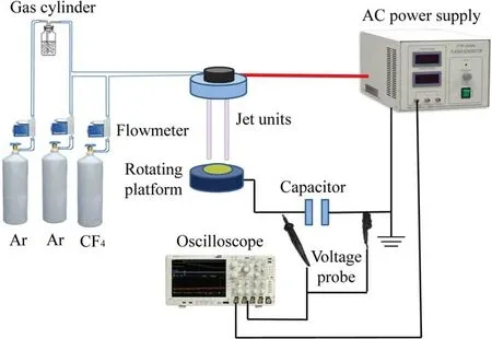
Figure 2.APPJ modification experiment platform.
In this paper,the plasma silicon plating method is used as follows:TEOS is used as the precursor,and the argon gas,with a 1 l min−1flow rate,as the carrier gas to pass through the jet tube.Another agron gas circuit is directly introduced into the jet tube with a 10 l min−1flow rate.The plasma is generated using the 5 kV,50 kHz high-frequency highvoltage power supply and silicon-containing film is deposited on the sample under the jet tube.The plasma silicon plating time is 30,60,90 and 120 s.In a similar way,the plasma fluorination method is used as follows:the CF4gas is used as the precursor and the argon gas is directly introduced into the jet tube with a 1 l min−1flow rate.The plasma used the 4.5 kV,50 kHz high-frequency and high-voltage power supply and fluorine is grafted on the sample surface.The plasma fluorination time is 30,60,90 and 120 s.
Considering that the electrode structure of flashover voltage in this paper is the needle-needle electrode,the gas–solid-conductor triple junction will accumulate a large number of surface charges and severely distort the electric field,where it has rather higher field strength than the area between the electrodes and it should be treated separately[30,31].Therefore,the field intensity distribution formed by this electrode can be characterized into the high field strength area(near the tip of the needle)and the low field strength area(between the two needles).Thus,the sample in this paper will be artificially separated into the high field strength treatment area(HFSTA)and low field strength treatment area(LFSTA),as shown in figure 3(a).The distance between the two needles is 7 mm and the LFSTA width is 4 mm located in the middle of the two needles.In addition,the width of each HFSTA is 1.5 mm located near the tip of the needle.Two types of regions are modified using different plasma treatment methods.As an example shown in figure 3(b),the plasma fluorination is applied in the LFSTA when silicon plating is applied in the HFSTA,correspondingly.

Figure 3.Schematic diagrams of the step gradient modification.(a)Different treatment region and(b)different plasma treatment methods.
In addition,when one area is modified,the other area will be covered using the shielding device to prevent the interference of the different modification methods.To ensure the same modification effect on the two separated HFSTA areas,a shunt device is installed on the jet electrode and two jet pipes are used to modify the two areas at the same time with the flow rates of the precursor and discharge gas as 2 and 20 l min−1,respectively.
2.2.Flashover voltage test platform
The surface flashover testing platform of epoxy resin includes a stainless-steel experimental chamber,needle-needle stainless-steel electrodes,high-voltage DC power supply(0 to−50 kV),multi-functional oscilloscope(Tektronix DPO 2002B),high-voltage probe(Tektronix,P6015A)and protection resistance(1 MΩ).The experimental device is shown in figure 4.To fully investigate the step gradient modification effect on the electric field distribution,the surface flashover voltage is measured by the needle-needle electrode,which can generate an extremely non-uniform electric field.One of the needle electrodes is attached to a conductive device,which is across the chamber and this device is connected in series with the power supply through a protection resistance.Another needle electrode and chamber are grounded together and the distance between the two needles is kept as 7 mm.

Figure 4.Flashover voltage experiment platform.
Before testing,the sample is placed close to the bottom of the electrodes through the motion device built in the chamber and the flashover experiment is conducted at 24 °C with a relative humidity of 30%.During the flashover testing,the negative voltage rises at the rate of 0.5 kV s−1until the flashover occurs.The high-voltage probe and oscilloscope capture the waveform and flashover voltage.Each sample is tested ten times and the average value is taken as the sample’s flashover voltage.
2.3.Surface charge measurement platform
As shown in figure 5(a),the surface charge measurement platform contains two parts.One measures the sample surface potential decay at a certain point after corona charging.The other one measures the whole sample surface potential distribution after charging with the flashover electrodes.When measuring the surface potential decay of a single point,the stainless-steel pin is applied with the −7 kV DC high-voltage and the distance between the tip of the pin and the sample is 7 mm.After charging for 60 s,the charging pin is removed and an electrostatic probe is moved to 2 mm above the measuring point through the 2D motion equipment.The surface potential decay data for 1800 s is recorded using an electrostatic potentiometer and capture card.When measuring the surface potential distribution,the sample is charged using the needleneedle electrodes,which are used to test the flashover.After charging with −7 kV DC high voltage for 300 s,the sample is moved to the surface charge measurement platform and scanned with the electrostatic probe.The scanning path is shown in figure 5(b)and the route is controlled by a special program to ensure that the whole sample will be scanned.The scan area is a square with sides 40 mm long.The measured data are in the form of a dot array with 21 rows and 21 columns.These dot array data will be plotted as the cloud picture using MATLAB software,within which the surface potential distribution will be displayed.This measurement method simulates the sample surface charge accumulation before the flashover.

Figure 5.Surface charge measurement platform.(a)Measuring device and(b)schematic diagram of the scanning path.
3.Results and discussion
3.1.Characterization
According to figure 3(b),the sample surface is separated into two regions(three parts).The step gradient modification method therefore can be separated as F-Si-F and Si-F-Si.The corresponding treatment time of the plasma fluorination and silicon plating is 30,60,90 and 120 s,respectively.Figure 6 shows the actual Si-F-Si sample image together with the SEM image and XPS spectra.Figure 6 also shows that the plasma silicon deposition areas have thin films,while the plasma fluorination area is not clear.The SEM image shows the boundary of two areas.It is found that there are significant differences between these areas of silicon deposition and fluorination.The XPS spectra at different modified areas indicate that the Si and F elements have been successfully grafted.

Figure 6.Characterization of the Si-F-Si sample.
3.2.Flashover voltage
In order to compare the effect of the different step gradient modification on the flashover voltage more clearly and to compare it with the untreated sample and traditional single plasma modification,figure 7 shows the flashover voltage of all samples,where the untreated sample flashover voltage is 9.45 kV,the voltage of the sample treated using APPJ fluorination is 9.68 kV and the voltage of the sample treated using APPJ silicon deposition is 10.76 kV.It is found that the flashover voltage of the Si-F-Si combination(up to 12.32 kV)is higher than the other samples.Although the modification effect of the F-Si-F combination is better than that of the untreated and single modification samples,the overall improvement effect is not obvious and the flashover voltage(only 10.17 kV)is generally lower than the Si-F-Si combination.Furthermore,there seems to be no obvious laws applicable to the different combinations on the flashover.

Figure 7.Flashover voltage of all samples.
3.3.Surface potential
The insulating material flashover voltage highly depends on the surface charge and the surface charge dissipation rate is proportional to the surface potential decay[18].A sample processed with step gradient modification can be separated into three areas as the untreated area,fluorination area and silicon deposited area.Each area will select a point to be measured and each sample measures only one point to ensure experimental accuracy.The single point surface potential decay of the samples with different treatment methods is shown in figure 8.It is found that both plasma fluorination and silicon deposition can accelerate the decay rate.The surface potential decay rate of the sample with silicon deposition is clearly faster than that of the sample with fluorination.According to the isothermal surface potential decay theory[21],the trap-level distribution curves of the samples before and after treatment are shown in figure 9.Note that the two kinds of plasma treatment can introduce shallow traps.The density of the shallow traps processed with plasma silicon deposition is higher and the energy level is lower.It can be inferred that the surface charge dissipation rate can be controlled by different plasma treatments.

Figure 8.Surface potential decay curve of the samples with different plasma treatments.

Figure 9.Trap-level distribution curves of the samples with different plasma treatments.
The surface potential distributions of the whole sample after needle-needle electrode charging are shown in figure 10.The figures are 3D graphs.The X-axis and Y-axis represent the positions of the sample surface,while the Z-axis represents the surface potential at a certain location.The different colors represent different surface potential values,which clearly display the surface potential distribution.It can be inferred that untreated sample surface charges accumulate near the tips of the two needle electrodes,while the F-Si-F treated sample surface charge distribution is more dispersed.In comparison,the surface charge distribution of the Si-F-Si treated sample is the most uniform one.
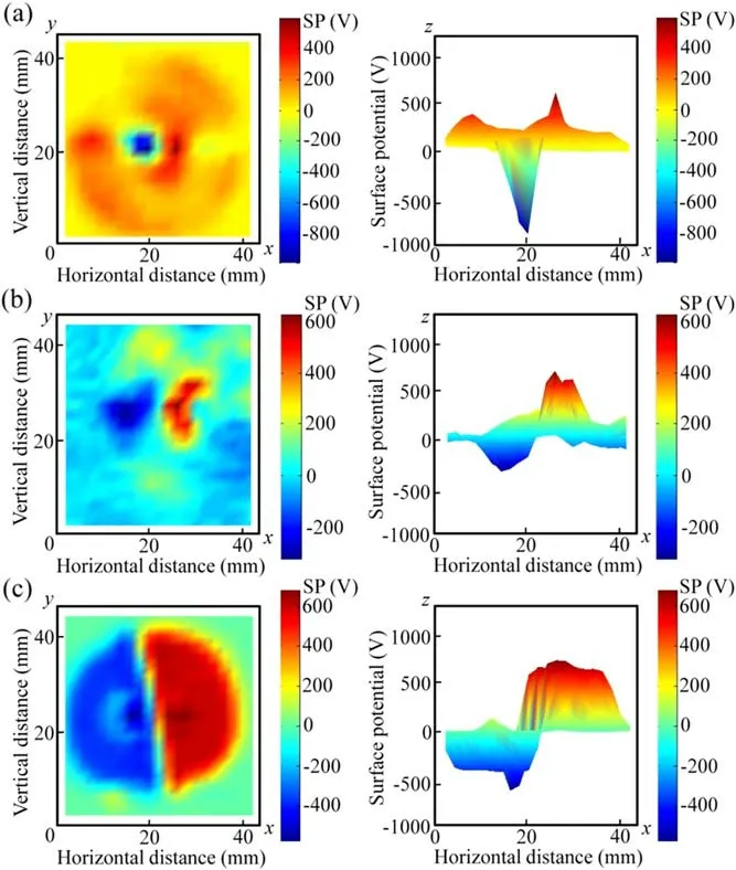
Figure 10.Sample surface potential distribution after needle-needle electrode charging.(a)Untreated sample,(b)F-Si-F sample and(c)Si-F-Si sample.
According to[32,33],most of the surface charges accumulated near the three-junction-point during charging.Increasing surface conductivity and introducing shallow trap can accelerate the migration and suppress local charge accumulation.We measured the surface conductivities of the sample with single plasma modification and the results are presented in figure 11.The surface conductivities of the fluorination and silicon deposition treated samples increase by two and three orders of magnitude,respectively.Considering plasma treatment increases the shallow trap density,as shown in figure 9,it can be concluded that the change of surface potential distribution,caused by the plasma fluorination and silicon deposition,increases the surface conductivity and introduces shallower traps,which accelerates surface charge migration and inhibits charge accumulation.Less surface charge accumulation means that surface charges have less distortion to the electric field,hence the flashover is suppressed.

Figure 11.Surface conductivity of the untreated and single treated samples.
3.4.Simulation of the step gradient modified electric field
To explain the different effects of the different step gradient modification methods on the flashover voltage,COMSOL Multiphysics software is used to build the needle-needle electrode finite element model.It simulates the charge transfer based on the dilute material transfer field.The influences of the different surface conductivity values on the field strength distributions are compared and analyzed in our work.
Because the electrostatic module is applied,the electric field distribution in space with charge ρvcan be calculated by the Poisson equation as,
and the space charge in gas(ρv)is determined by the densities of the positive and negative ions(n+and n−)as,

The charge density of the gas–solid interface can be calculated by the continuous boundary field conditions as,
where ρ is the surface charge density and n is the normal vector.D1and D2are the electric displacements on the opposite sides of the interface.The changing rate of ρ consists of three components,including volume-side current(Jv),gasside current(Jg)and surface current(Js).Jgis formed by the free diffusion and field migration as,
where the first term represents the conduction current in gas generated by the electric field(En),which is determined by the field-induced mobilities(b−,b+)and gas ion concentration(c−,c+).The second term is the equivalent current generated by the gas ion free diffusion,which is related to the gas ion diffusion coefficient(D−,D+).

where Jsis determined by the surface conductivity(γ0)and the tangential electric field(El).ksis used to characterize the sensitive response of the surface conductance to the field.
where Jvis related to the volume conductivity of the solid materials γv.All three currents can describe the charge accumulation process.
Considering space charge transfer in gas,the diffusion process is calculated by using the dilute material transfer field.For example,the equation of positive ions is,
where kcis the recombination coefficient of air[34].
In order to compare the different effects of the single conductivity distribution and step surface conductivity distribution on the electric field strength,the surface conductivity parameters of the model are set as the step function to realize precise surface conductivity control.According to the flashover voltage tests,the single conductivity values are set as 1×10⁻¹⁷S and 1×10⁻¹⁶S.Correspondingly,the step surface conductivity value is set as 1×10⁻¹⁵S–1×10⁻¹⁷S–1×10⁻¹⁵S,and the width of the different surface conductivity is equal to the parameter of the HFSTA and LFSTA.The simulation of the needle-needle electrode electric field intensity under different conductivity distributions is shown in figure 12.According to[31],the maximum field strength determines the probability of the insulation failure.The values of the maximum field strength with single conductivity distribution are 11 and 25 MV m−1,respectively,while the value with the step gradient conductivity distribution is only 5.5 MV m−1.Therefore,the maximum field strength can be significantly reduced by using the step gradient conductivity distribution and the field strength distortion at the triple junction point can be weakened,thus affecting the surface flashover.
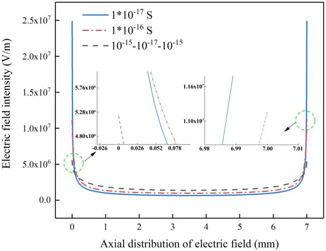
Figure 12.Simulation of the needle-needle electrode electric field intensity with different surface conductivities.
3.5.Mechanism of the step gradient modification
According to section 3.3,the surface conductivity increase can accelerate the surface charge dissipation,reduce the distortion of electric charge to field strength and subsequently decrease the flashover voltage.However,if the surface charge dissipates too fast,it will provide seed charge for the flashover formation and development promoting the flashover occurrence[35–37].In addition,the charge accumulation degree at different positions of the electrodes is different,which requires different charge dissipation rates at different positions.Therefore,it is difficult to consider the different charge dissipation requirements using a single modification method on the insulating materials.In our case,a large amount of surface charge will be accumulated at the three junction points of the needle-needle electrode used for the surface flashover.But the electric field strength between the electrodes is lower and the charge accumulation is less.Therefore,this work separated the sample into the HFSTA and LFSTA to obtain the differences in the charge dissipation rate.
From the compared results of the flashover voltage,the step gradient modification method can change the material surface conductivity with the step gradient distribution and the flashover voltage improved compared with the single modification sample.Furthermore,the effect of the Si-F-Si combination on the flashover voltage is better than the F-Si-F combination.This is because the silicon plating can improve the surface conductivity of the epoxy resin to a greater extent,which accelerates the charge dissipation at the three junction points and weakens the charge distortion effect on the field strength.The small surface conductivity increase due to fluorination in the LFSTA can alleviate the excessive charge dissipation in the HFSTA and inhibit the discharge development process.However,if the surface conductivity in the HFSTA is not sufficient,the charge dissipation at the triple junction points will be slow.There will still be a large amount of charge causing the electric field distortion.So there will be no clear improvement effect on the flashover voltage.
4.Conclusion
In this paper,the step gradient modification of the epoxy resin was achieved with the APPJ jet platform.The surface flashover voltage and surface charge characteristics of the plasmatreated samples were measured.The influence mechanism of the plasma step gradient modification on the surface flashover was numerically investigated using COMSOL simulation software.The main conclusions are as follows.
(1)The flashover voltage of the sample with the plasma step gradient modification is better than the unmodified sample(increased by 30%)and the single modified sample(at most increased by 27%).
(2)The field intensity distribution of the needle-needle electrode can be separated as the high field intensity area(at three junction points)and low field strength area(between electrodes).The step gradient modification can accelerate the charge dissipation at the high field strength region and the dissipation speed at the low field strength region can be properly controlled.The flashover voltage of the step gradient modified sample increased.
(3)According to the surface charge accumulation results,the surface charge distribution is made more uniform by using the plasma step gradient modification and the surface charge distortion effect on the external electric field is suppressed.
(4)According to simulation results,when the sample surface conductivity is optimized as a step gradient distribution,the maximum field strength exerted by the needle-needle electrodes is effectively reduced and the flashover occurrence is inhibited.
Acknowledgments
This work was supported by National Natural Science Foundation of China(No.51777076),the Self-topic Fund of State Key Laboratory of Alternate Electrical Power System with Renewable Energy Sources(No.LAPS2019-21).
猜你喜欢
杂志排行
Plasma Science and Technology的其它文章
- Special issue on selected papers from HVDP 2020
- Microwave transmittance characteristics in different uniquely designed one-dimensional plasma photonic crystals
- Burst pulses for positive corona discharges in atmospheric air:the collective movement of charged species
- Reconstruction of energy spectrum of runaway electrons in nanosecond-pulse discharges in atmospheric air
- The enhanced aerosol deposition by bipolar corona discharge arrays
- Effect of dilution gas composition on the evolution of graphite electrode characteristics in the spark gap switch