Optical polarization characteristics for AlGaN-based light-emitting diodes with AlGaN multilayer structure as well layer∗
2021-05-06LuXue薛露YiLi李毅MeiGe葛梅MeiYuWang王美玉andYouHuaZhu朱友华
Lu Xue(薛露), Yi Li(李毅), Mei Ge(葛梅), Mei-Yu Wang(王美玉), and You-Hua Zhu(朱友华)
School of Information Science and Technology&Tongke School of Microelectronics,Nantong University,Nantong 226019,China
Keywords: AlGaN-based quantum well,method,internal quantum efficiency,degree of polarization
1. Introduction
AlGaN-based deep ultraviolet (DUV) light-emitting diodes(LEDs)have attracted much attention due to their broad application prospects in water purification, sterilization, skin therapy, etc.[1–4]To date, the external quantum efficiency(EQE) of AlGaN-based DUV LED bare die with a p-GaN contact layer is generally less than 7%at 250 nm–280 nm.[4]Compared with blue LED,AlGaN-based DUV LED has high acceptor ionization energy, strong absorption in the p-GaN contact layer, and unique polarization characteristics, which makes it have lower EQE.[5,6]In order to solve these problems,many methods have been used to improve the luminous efficiency of AlGaN-based DUV LED. For example, by employing several features,such as the AlGaN:Mg contact layer and Rh mirror electrode, Takano et al. reported that a maximum EQE of more than 20% can be obtained at 275 nm.[7]Wang et al. proposed an ultrathin GaN/AlN multiple quantum wells(MQWs)structure with electron-beam pumping.[6]The output power of MQWs reached ∼2.2 W at 260 nm due to the reduction of quantum-confined Stark effect (QCSE) and the improvement of material quality and carrier injection. Zhang et al. proposed a DUV LED structure with air cavity extractor, which can significantly improve the extraction efficiency of TM/TE polarized light.[8]In addition, in order to improve the luminous efficiency of LED, other structure designs have also been reported in the literature,such as the multi-quantum barrier electron blocking layer structure,[9]the type-II QW structure,[5,10]AlN-delta-GaN QW structure,[11]step-like QW structure,[12,13]and Al composition-graded p-AlGaN cladding layer structure.[14]
In our previous work, we reported the effects of Alcontent in the barrier layer on the optical properties of Al0.35Ga0.65N/AlxGa1−xN QW structure.[15]By increasing the Al-content of barrier layer, the degree of polarization (DOP)can be greatly improved. However, the spontaneous emission rate for TM mode and TE mode decrease with the increase of Al composition in the barrier layer due to the larger polarization-induced electric field. Although the effect of the internal electric field on the electron–hole overlap can decrease by reducing the thickness of the well layer,the further improvement of the spontaneous emission rate will be limited due to the decrease of the electron-hole radiation recombination region.
In the present paper, we propose an AlyGa1−yNAlxGa1−xN-AlyGa1−yN/AlxGa1−xN QW structure. Here, the multilayer structure as the new well layer consists of two thin AlyGa1−yN well layers separated by a thin AlxGa1−xN isolation layer. Replacing a conventional well layer with two coupled well layers can not only suppress the QCSE, but also effectively increase the electron–hole recombination region.The numerical results show that the TE/TM polarized emission and internal quantum efficiency(IQE)can be significantly improved by using two coupled QW structures,while the DOP can be similar to that of conventional quantum well structure.
2. Theory


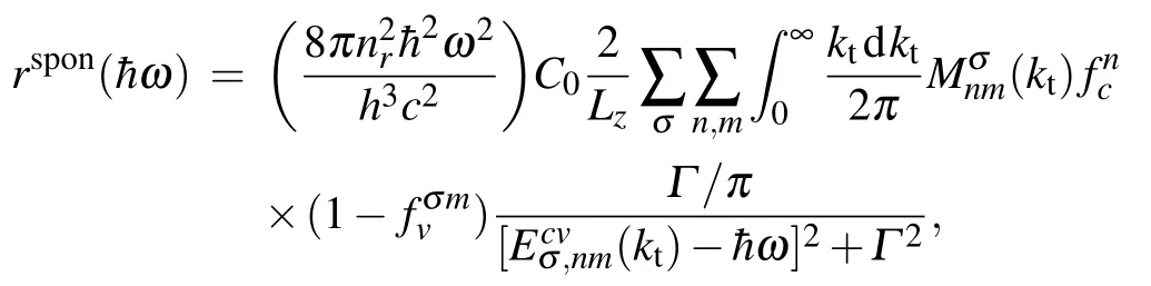
After obtaining the conduction band structure, the valence band structure,and the corresponding wave function,the spontaneous emission rate(rspon)was solved by the following formula:[19]
with

3. Results and discussion
In this work,the AlGaN-based LED with an AlGaN multilayer structure as the well layer is considered, including an n-type Al0.55Ga0.45N layer, a single QW (SQW) layer, and a p-type Al0.5Ga0.5N layer, which are shown in Fig.1. The SQW consists of an 8-nm-AlxGa1−xN barrier layer and two 1-nm-Al0.35Ga0.65N well layers separated by 2-nm-AlxGa1−xN isolation layer. The barrier layer and the isolation layer have the same Al component,and the Al component x values are set to be 0.5 and 0.55,which are called samples A and A 1 respectively. For comparison,the conventional QW structures with 1 nm(sample B,B 1)and 2.5 nm(sample C,C1)Al0.35Ga0.65N well layer are also studied. The value of x in Al composition of the AlxGa1−xN barrier layer of samples B and C are both set to be 0.5, while that of samples B 1 and C1 are both set to be 0.55. The electron concentration and hole concentration of n-type and p-type layers are set to be 1.7×1018cm−3and 2.74×1017cm−3,respectively.

Fig.1. Schematic structure of samples A(A 1),B(B 1),and C(C1).
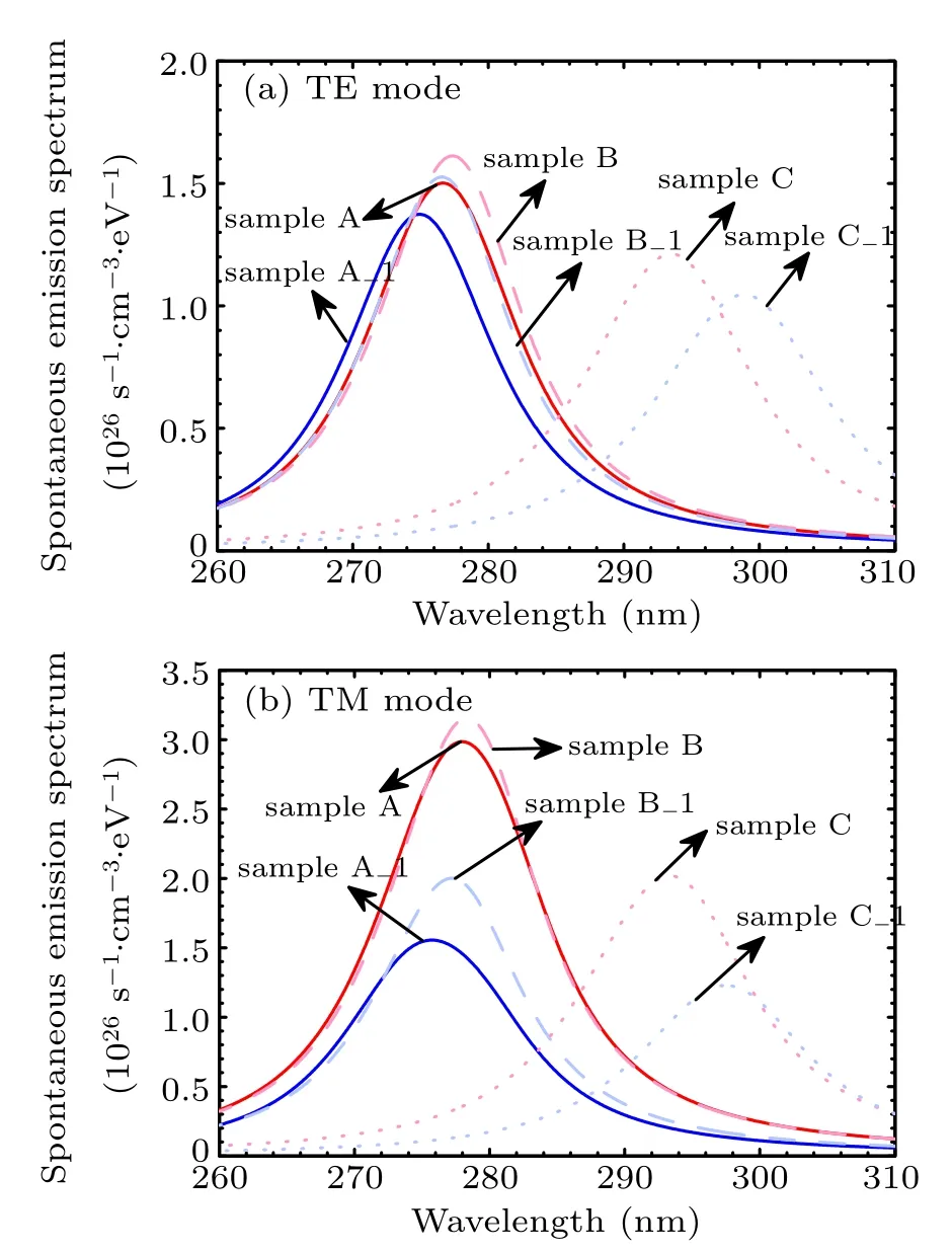
Fig.2.(a)TE-polarized and(b)TM-polarized spontaneous emission spectra of the samples A(A 1),B(B 1),and C(C1)at J=100 A/cm2.
Figure 3 shows TE-polarized and TM-polarized total spontaneous emission rate(Rsp)as a function of current density. As mentioned in our previous investigation,[15]the Rspfor TE mode and TM mode can be improved by reducing the Al content of the barrier layer, which is caused by the decrease of internal electric field. When the injection current density is greater than about 35 A/cm2,the TE-polarized and TM-polarized Rspof novel structure(sample A)are larger than those of the traditional quantum well structure (sample B). With the increase of Al-content of barrier layer, the TE-polarized Rspof the new structure (sample A 1) is obviously larger than that of the conventional structure (sample B 1) at J >56 A/cm2, while the TM-polarized Rspof sample A 1 is slightly larger at J >85 A/cm2. For example, at J = 100 A/cm2, the TE-polarized and TM-polarized Rspof sample A are increased by 12.7%(35.6%)and 17.7%(67.7%),compared with those of sample B(sample C), while those of sample A 1 are increased by 9.6%(44.3%)and 1.8%(51.1%)respectively compared with those of sample B 1(sample C1).The higher Rspfor the novel structure can be attributed to the strong quantum confinement and the wide recombination region.
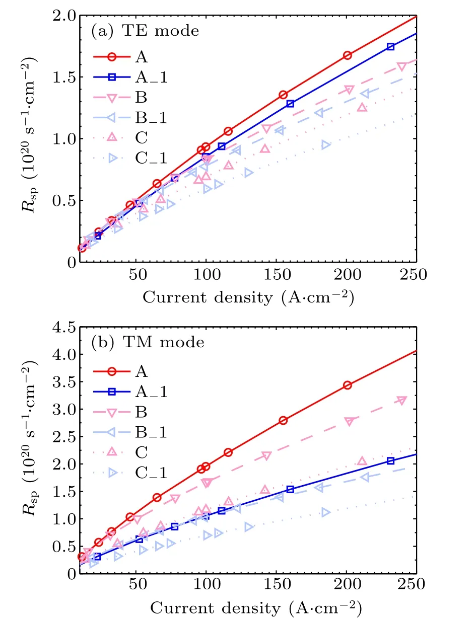
Fig.3.The total spontaneous emission rate(Rsp)for TE polarization(a)and TM polarization(b)as a function of current density.
Figure 4 shows the peak wavelength of TE-mode and TM-mode as a function of current density. It can be seen from the fgiure that the peak wavelength of TM-mode is greater than that of TE-mode,except samples C and C 1. At the injection current density of 100 A/cm2, the difference in peak wavelength between the TM mode and the TE mode increases from−0.14 nm(−1.3 nm)of sample C(C 1)to 1.36 nm(0.79 nm)of sample A(A 1). As shown in Figs. 5(b) and 5(c), the difference between c1–v2 and c1–v1 transitions at Γ point is obviously increased by reducing the well layer thickness of conventional QW structure.In this paper,the c1 and c2 denote the two lowest conduction subbands and the v1–v6 represent the top six valence subbands,obtained by using the upper Hamiltonian. For the novel structure, the transition energy levels extend to a wide energy range due to the coupling between well layers as shown in Fig.5(a). In addition, the dominant polarization properties of the transition energy levels are different, which can be inferred from the peak intensities of TE mode and TM mode in Figs. 5(d)–5(f). Thus, the difference in peak wavelength between the two polarization modes can be increased by the strong quantum confniement and the coupling between the well layers. It should be noted that the peak wavelength of TE mode for samples C and C 1 are longer than the peak wavelength of TM mode. Although the dominant polarization of c1–v1 and c1–v2 transitions of sample C(or C 1)are TM polarization and TE polarization respectively as inferred from Fig.5(f),the differences in peak intensity between TM mode and TE mode for both c1–v1 and c1–v2 transitions are much smaller than counterparts of sample B. In addition,for c1–v1 transition, the TE-mode peak wavelength is longer than TM-mode peak wavelength(not given here). These factors lead to longer peak wavelength of TE mode. It is also found that the peak wavelength of TM mode of sample A(A 1) is longer than that of sample B (B1) at low injection current density, while that of TE mode is shorter. It can be attributed to the coupling between the well layers, so that the energy level in the quantum well is split into a lower level and a higher level as shown in Figs. 5(a) and 5(b). Moreover, it can be inferred from Fig.5(d)that the c1–v1 transition and the c2–v1 transition have a TM-dominated polarization characteristic, while c1–v5 and c2–v2 have a TE-dominated polarization characteristic. Thus, the peak wavelength of TM mode of novel structure can be longer at the low injection current density. At high current density,the peak wavelengths of TM and TE modes of sample A(A1)are both shorter than those of sample B(B 1)due to the influence of the higher transition energy levels,such as c2–v1 and c2–v2 transitions.
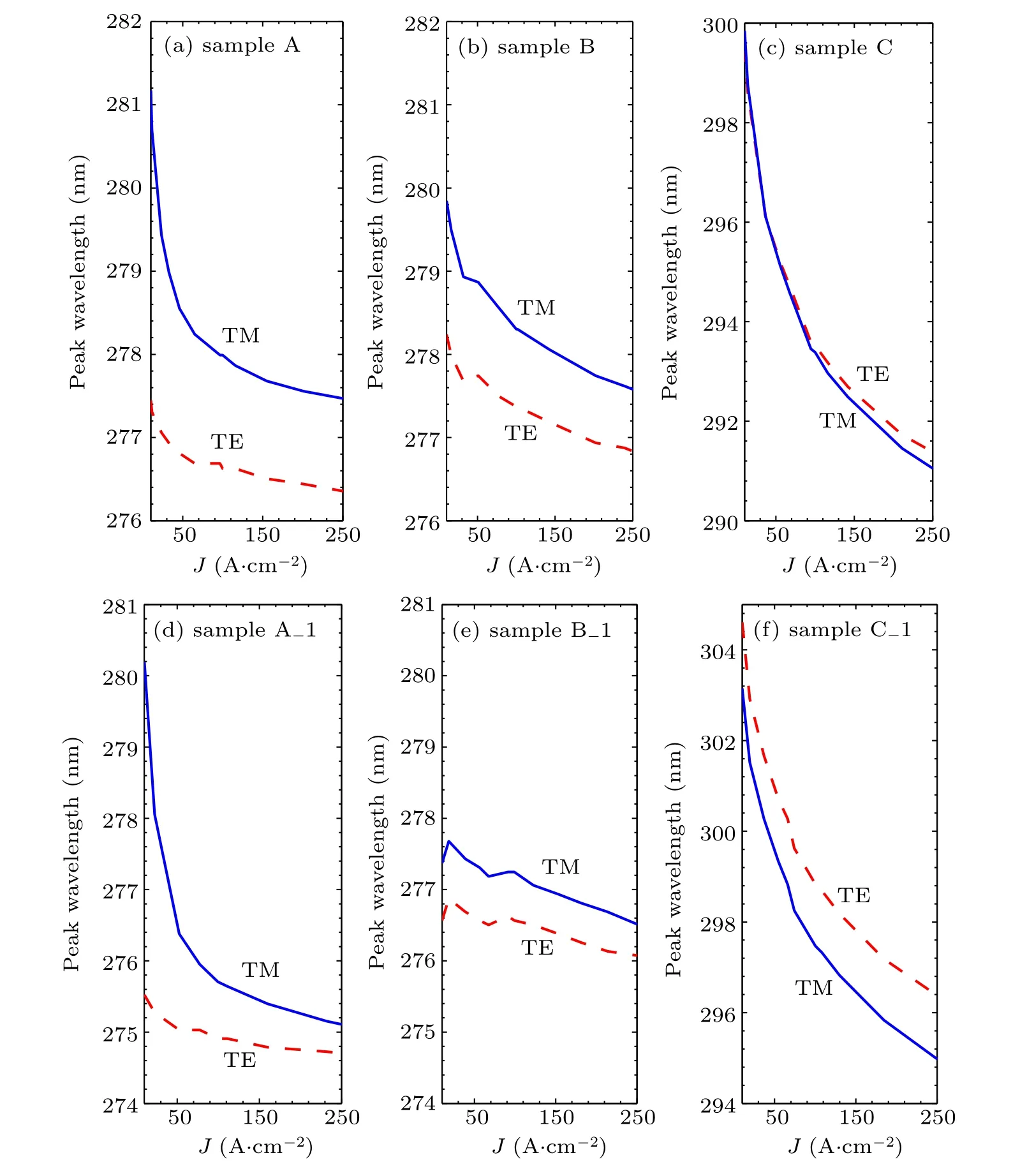
Fig.4. Plots of peak wavelength of TE mode and TM mode versus current density.

Fig.5. Plots of (a)–(c) transition energy and (d)–(f) peak intensity for the transitions between the conduction subbands (c1–c2 or c1) and valence subbands(v1–v6 or v1–v3)at J=100 A/cm2. These valence subbands are obtained by using upper Hamiltonian.
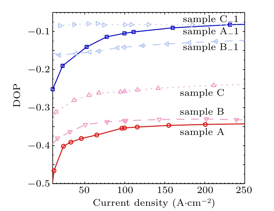
Fig.6. DOP values versus current density for samples A(A 1),B(B1),and C(C1).
Figure 6 shows the DOPs as a function of current density for samples A(A 1),B(B 1),and C(C1). The DOP can be calculated from ρ =(ITE−ITM)/(ITE+ITM), where ITEand ITMare the TE-polarized and TM-polarized Rsp,respectively.On the whole, the QW structure with high Al-content in the barrier layer has a larger DOP value as reported in Ref. [15].For the conventional QW structure, the DOP decreases with the well layer thickness decreasing from 2.5 nm to 1 nm.Comparing with sample C (C 1), the DOP of sample B (B1) is reduced by 0.06–0.09(0.08–0.04)in the investigated injection current density range. From Figs.5(e)and 5(f),it can be seen that the mixing of valence subbands seems to weaken with the decrease of well thickness,so that the c1–v1 transition of sample B is almost of TM polarization,while the c1–v2 transition is almost of TE polarization. Meanwhile,the difference in transition energy between c1–v1 and c1–v2 becomes larger.As a result, the DOP for the conventional QW structure can decrease by reducing the well thickness. Note that the DOP of sample C is basically consistent with the reported experimental result in Ref. [21] at J =100 A/cm2. For the novel structure, the DOP of sample A further decreases compared with those of samples B and C,while the DOP of sample A1 increases to a value close to the DOP of sample C 1 as the current density increases. From Fig.5(d) it can follow that the peak intensity of TM mode for the c1–v1 transition and the c2–v1 transition are much larger than the peak intensities of TE mode for all transitions. However, this situation does not occur for sample A 1 with high Al-content in the barrier layer as shown in Fig.7(a). The peak intensity of TE mode of c1–v4 transition for sample A 1 can be compared with that of TM mode of c1–v1 transition and c2–v1 transition, which is similar to that of c1–v1 transition and c1-v3 transition for sample C 1. Thus,the DOP of sample A can further decrease,while the DOP of sample A 1 is close to that of sample C1 at the larger current density.
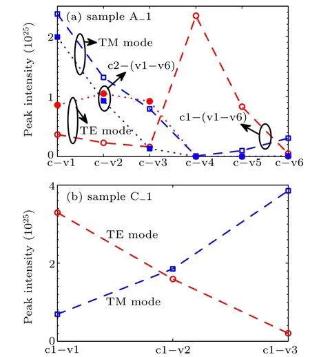
Fig.7. Peak intensities of TE mode and TM mode for transitions between the conduction subbands(c1–c2 or c1)and valence subbands(v1–v6 or v1–v3)at J=100 A/cm2 for(a)sample A 1 and(b)sample C1.
Finally, the internal quantum effciiency for each of samples A (A 1), B (B 1), and C (C1) as a function of current density is investigated, and the results are shown in Fig.8.The IQE is defnied as η =Rcr/(Rcr+Rnonr+RAug).[19]At an injection current density of 100 A/cm2,it can be observed that the IQE is enhanced from 13.6% (10.1%) of sample C (C1)to 20.5%(14.8%)of sample A(A 1). It should be noted that the calculated IQE is low,which can be attributed to two factors. One is due to the large Auger coefficient and small SRH recombination lifetime employed in the calculation. According to the reports in the literature,[22,23]the Auger coefficient can be increased from ∼10−31cm6/s to ∼10−30cm6/s due to the defect-assisted Auger recombination, which will lead the IQE to significantly decrease. The other is that the average value Rcrof AlGaN-based LED is lower due to its polarization characteristics than that of visible light GaN-based LED.In addition,it is also seen that the effciiency droop effect can be obviously suppressed by using the novel QW structure. For example, the IQE of sample A (A 1) from J =10 A/cm2to J =250 A/cm2is reduced by 30.6% (33.3%), while that of samples B (B 1) and C (C1) are reduced by 48.1% (52.2%)and 48.5% (49.87%), respectively. Comparing with the traditional structure, the performance improvement of the new structure is attributed not only to the enhancement of spontaneous emission rate,but also to the decrease of Auger recombination rate due to the wide recombination region.

Fig.8. Plots of internal quantum efficiency of AlGaN-based QW structure versus current density for various samples.
4. Conclusions
In this work, the optical properties of AlGaN-based QW structure with two coupled thin well layers are investigated by using the effective mass theory. As the current density is greater than a certain value,the TE-and TM-polarized Rspof sample A(A 1)are larger than those of samples B(B1)and C(C1)due to the strong quantum confniement and the wide recombination region. At J=100 A/cm2,the difference in peak wavelength between TM mode and TE mode increases from−0.14 nm(−1.3 nm)of sample C(C 1)to 1.36 nm(0.79 nm)of sample A (A 1), while the peak wavelength of sample A(A 1)is shorter than the peak wavelengths of samples B(B1)and C(C1). For the conventional QW structure,the DOP of sample B(B 1)is reduced by 0.06–0.09(0.08–0.04)at J=10–250 A/cm2compared with that of sample C(C 1),due to the reduction of well layer thickness. For the novel structure,the DOP of sample A is further decreased compared with that of samples B, while the DOP of sample A 1 is close to that of sample C 1 at the larger current density. It can be attributed to the band adjustment caused by the combination of barrier height and well layer coupling. By employing the coupled well layer, the IQE of sample A (A 1) is also increased to 20.5%(14.8%)at J=100 A/cm2. In addition, the effciiency droop effect can be expected to be suppressed by using the novel structure.
猜你喜欢
杂志排行
Chinese Physics B的其它文章
- Quantum annealing for semi-supervised learning
- Taking tomographic measurements for photonic qubits 88 ns before they are created*
- First principles study of behavior of helium at Fe(110)–graphene interface∗
- Instability of single-walled carbon nanotubes conveying Jeffrey fluid∗
- Relationship between manifold smoothness and adversarial vulnerability in deep learning with local errors∗
- Weak-focused acoustic vortex generated by a focused ring array of planar transducers and its application in large-scale rotational object manipulation∗