Snapback-free shorted anode LIGBT with controlled anode barrier and resistance∗
2021-03-11ShunLi李顺JinShaZhang张金沙WeiZhongChen陈伟中YaoHuang黄垚LiJunHe贺利军andYiHuang黄义
Shun Li(李顺), Jin-Sha Zhang(张金沙), Wei-Zhong Chen(陈伟中),2,†,Yao Huang(黄垚), Li-Jun He(贺利军), and Yi Huang(黄义)
1College of Electronics Engineering,Chongqing University of Posts and Telecommunications,Chongqing 400065,China
2Institute of Microelectronics,Chinese Academy of Sciences,Beijing 100029,China
Keywords: shorted anode lateral-insulated gate bipolar transistor,snapback,barrier,trade-off
1. Introduction
Lateral insulated gate bipolar transistor(LIGBT)is a popular power device due to its voltage control and low power loss at forward conduction,which is widely used in the field of the power integrated circuits.[1–9]However,the excessive carriers in the N-drift lead to the large turn-off loss Eoff.[10–17]The shorted anode (SA) LIGBT can effectively accelerate the extraction of electrons by introducing the N+anode in anode.[18]However, the snapback effect is induced when the working mode of the device transforms from unipolar mode to bipolar mode. In order to solve this problem, several novel structures have been proposed. The separated shorted anode(SSA)LIGBT is adopted to suppress the snapback by controlling the distance between N+anode and P+anode.[19]The trench shorted anode(TSA)LIGBT is proposed to alleviate the snapback by inducing an oxide trench between N+ anode and P+anode, which extends the path of the electrons.[20]The segmented trench in the anode region(STA)LIGBT can avoid the snapback by inducing a deep trench in anode.[21,22]The multiple current plugs(MCP)LIGBT can eliminate the snapback by introducing three separated current plugs into N-buffer.[23]
In this work, a novel SA LIGBT featuring a controlled anode barrier and resistance(CBR)is proposed and discussed to achieve the snapback-free and better trade-off characteristic between Vonand Eoff. The devices simulation results and validations are obtained by the TCAD MEDICI tools,and the parallel field mobility model,concentration-dependent model, perpendicular electric field mobility model, auger recombination, and Shockley–Read–Hall recombination model are adopted.[24]
2. Device structure and mechanism
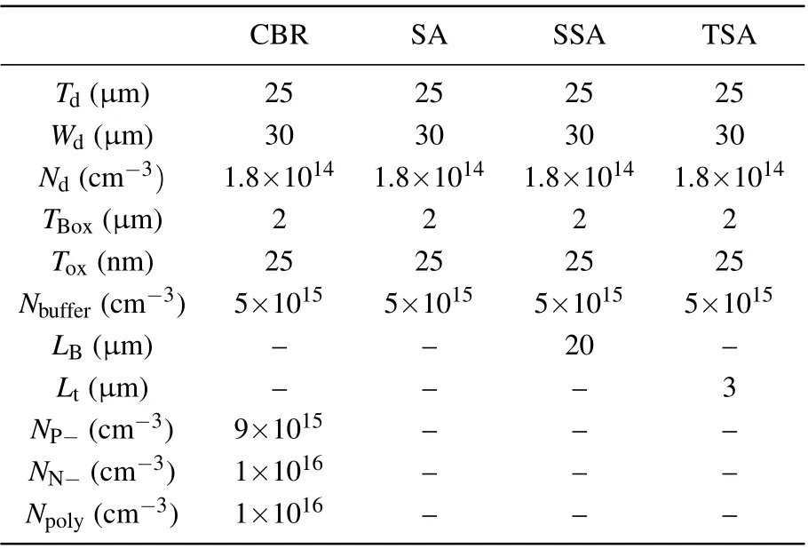
Figure 1(a) shows the schematic views of the CBR LIGBT. An oxide trench is set to be in anode region, which divides the N-drift into two parts. The P-float is set to be on the left of the oxide trench, which forms an electron barrier Vbarrierto inhibit the electrons from flowing into the N+anode.The N-type doping polysilicon layer is located on the top of the oxide trench, while the N-float is set to be on the right of the oxide trench,which forms the anode resistance RSAin series.The key parameters for the different structures compared with each other in this paper are listed in Table 1,where t and Npolyare the thickness and doping concentration of the polysilicon layer, respectively; NP−and NN−are the doping concentrations of the P-float and N-float,respectively;LBis the distance between N+anode and P+anode of the SSA LIGBT;Ltis the length of oxide trench of the TSA LIGBT.
Figure 1(b) shows the equivalent circuit and operating mechanism of the CBR LIGBT.The polysilicon layer and Nfloat are respectively regarded as the R1and R2in series,while the P-float is an electron barrier to block electrons flowing into the N+anode. The height of the potential barrier Vbarrieris expressed as

where niis the intrinsic carrier concentration, Nbufferis the doping of the N-buffer, NP−and k0are the doping of the Pfloat and Boltzmann constant,respectively.

Fig.1. (a) Schematic diagram of CBR LIGBT, Ndrift doping Nd =1.8×1014 cm−3,N-drift length Wd=30µm. (b)Equivalent circuit and operating mechanism of CBR LIGBT in unipolar mode.

Table 1. Key parameters of different LIGBTs.
The value of R1and R2can be obtained from


where Lpolyand LN−are the length of the polysilicon layer and N-float,respectively,tnis the thickness of the N-float,and Z is the length of the device in the vertical direction. Thus,the proposed device obtains a larger RSAthan the SA LIGBT.At the initial forward conduction stage (IA·RSA<0.7 V),the device operates in unipolar mode with single electrons,and the P-body/N-drift/P+ anode triode is turned off. When IA·RSA≥0.7 V, the PNP transistor is turned on, and the P+ anode injects holes into the N-drift. The device works in the bipolar mode. When the device transforms from unipolar mode to bipolar mode,the turnover voltage of snapback effect VSBcan be approximated as the following expression:[25]

where Rdand Rchare the resistance of N-drift region and channel,respectively;RSAcan be calculated from

So, the snapback VSBcan be suppressed by increasing the Vbarrier,R1or R2in the anode.
At turning off stage, the N-buffer/P-float/Polysilicon layer/N-float forms a low-resistance path to accelerate the extraction of electrons,which effectively reduces the Eoffof the CBR LIGBT.
3. Results and discussion
3.1. Forward conduction characteristics
Figure 2(a) shows the comparison of forward conduction characteristics among the CBR LIGBT,SA LIGBT,SSA LIGBT,and TSA LIGBT.For the SA LIGBT,it switches from unipolar mode to bipolar mode with abrupt voltage due to the shorted effect of the N+ anode. Thus it exhibits the most serious snapback phenomenon in all the LIGBTs above. For the SSA LIGBT, it still suffers a tiny snapback even if the LBincreases to 20 µm, which leads to the waste of the chip length. For the TSA LIGBT, the snapback effect can be effectively suppressed when the oxide trench is deep enough(Lt≥3 µm). The CBR LIGBT achieves the snapback-free characteristic, because the RSAand the Vbarriercan be easily increased by adjusting the doping concentration of polysilicon layer and P-float. Additionally,both the CBR LIGBT and TSA LIGBT achieve the lowest voltage drop of 1.12 V at JAof 100 A/cm2.
Figure 2(b) shows the current distributions in the anode region of the CBR LIGBT at points A and B. At point A of JA=3 A/cm2, the device operates in a unipolar mode, and the P+ anode/N-buffer junctions is turned off. The electron current flows to the N+ anode along the path of N-buffer/ Pfloat/Polysilicon layer/N-float. At point B of JA=40 A/cm2,the P+anode/N-buffer junction is turned on,and the P+anode begins to inject holes into the N-drift. The device mode transforms into bipolar mode with exponentially increased current.

Fig.2. (a)Forward conduction characteristics of CBR LIGBT,SA LIGBT,SSA LIGBT (LB =20 µm), and TSA LIGBT (Lt =3 µm), with voltage applied to the gate Vgate being 15 V, and cathode connected to the ground Vcathode=0 V.(b)Current distributions in anode at points A and B of CBR LIGBT(points A and B are shown in(a)).

Fig.3. Forward conduction characteristics of CBR LIGBT (a) at different values of Npoly,NN−,and(b)NP−.
Figure 3 shows the forward conduction characteristics of CBR LIGBT at different values of NP−,NN−,and Npoly. Obviously, the decreasing of Npolyand NN−are favorable for suppressing the snapback because the R1and R2are increased as shown in Fig.3(a). In Fig.3(b), increasing NP−is helpful in suppressing the snapback because the Vbarrieris increased according to Eqs. (1) and (4). Moreover, the inhibition effect of NP−and Npolyon snapback are more obvious than that of NN−. So adjusting NP−and Npolyare a promising method to eliminate the snapback phenomenon.
Figure 4 shows the influences of Npolyon forward voltage drop Vonat different temperatures T of CBR LIGBT.For the given T, both the Vonand ∆VSBgradually increase with Npolyincreasing, and it also illustrates that reducing Npolyis beneficial to solving the snapback problem and reducing the Von. In addition, at the same Npoly, Vondecreases obviously with the increase of T, and a higher temperature is also easier to achieve the snapback-free characteristic. This is because the mobility decreases with the increase of temperature,which leads to a larger RSAfor the CBR LIGBT.At T =400 K,the device exhibits snapback effect only at Npolyof 1×1018cm−3.

Fig.4. Influences of Npolyon forward voltage drop Von at different temperatures of CBR LIGBT, with Von calculated at anode current density of 100 A/cm2.
3.2. Turn off characteristics
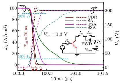
In Fig.5 the turn-off characteristics of different LIGBTs are compared among each other. All the devices are compared mutually at the same Vonof 1.3 V.The turnoff time Toffis calculated from 90%IAto 10%IA. For the SSA LIGBT,it shows the longest Toffof 570 ns, because a long LBis designed to suppress the snapback and also reduce the Von, resulting in a long extraction path with high resistance at turn-off stage. For the TSA LIGBT,it has Toffof 160 ns, because the trench oxide in anode will prevent the electrons from being extracted.The Toffof SA LIGBT is 90 ns,which is slightly slower than that of the CBR LIGBT. This is the result of a long and high doping concentration P+ anode necessary to achieve the Vonof 1.3 V,which is not conducive to the extraction of electrons.For the CBR LIGBT,it achieves the shortest Toffof 70 ns,because the N-buffer/P-float/polysilicon layer/N-float provides a low-resistance path to accelerate the extraction of electrons in N-drift.
Figure 6 shows the distributions of the electron concentration Neof different LIGBTs (y=4 µm) from t1to t4period, and the devices start to be turned off at t1period. At t2and t3periods,the Neof CBR LIGBT is lower obviously than that of the SSA LIGBT and TSA LIGBT.At t4period,the SA LIGBT and CBR LIGBT have completed the turn-off process,while there remain a lot of electrons in SSA LIGBT and TSA LIGBT.

Fig.5. Turn-off characteristics of different LIGBTs at the same Von of 1.3 V,obtained in the same circuit with bus voltage (Vbus) 200 V, gate resistance(Rg)10 Ω,load inductance(LC)10µH,and stray inductance(Ls)10 nH.

Fig.6. Distributions of electron concentration Ne along x direction(y=4µm)of different LIGBTs at(a)t1 period,(b)t2 period,(c)t3 period,and(d)t4 period. (Curves at period t1–t4 are shown in Fig.5).

Fig.7. Turn-off characteristics of CBR LIGBT(a)at different values of Npoly and(b)different values of NP−.
Figure 7(a) shows the turn-off characteristics of CBR LIGBT at different values of Npoly. The CBR LIGBT has a Toffof 390 ns at an Npolyof 1×1015cm−3. The Toffdecreases gradually with Npolyincreasing due to R1decreasing,thus the turn-off loss Eoffcan be further reduced. Figure 7(b) shows the turn-off characteristics of CBR LIGBT at different values of NP−. The Toffdecreases from 390 ns to 160 ns with NP−decreasing form 2.5×1016cm−3to 1×1016cm−3due to the enhanced Vbarrier. Furthermore, a reasonable Npolyor NP−is important to obtain a better trade-off between Vonand Eoff.
3.3. Trade-off characteristic
Figure 8 displays the influences of Npolyand L on ∆VSBand Eoff. For the device with Npolyof 1×1015cm−3,it shows that the snapback-free characteristic occurs with the increase of L. However, it also results in a large Eoff. For the device with Npolyof 1×1016cm−3and 1×1017cm−3, the ∆VSBincreases with L increasing,and a higher Npolywill bring a larger∆VSB. On the other hand,the Eoffdecreases with the increase of L, and increasing Npolyis beneficial to obtaining a lower Eoff. Because L can be regarded as the width of the cross section of electron path from P-float to polysilicon layer,increasing L leads to a narrower path for electrons, which is helpful in reducing the value of Eoff.

Fig.8. Influences of Npoly and L on ∆VSB and Eoff of CBR LIGBT, with L shown in Fig.1(b).

Fig.9. Trade-off characteristics between Von and Eoff, showing (a) influences of Npoly and t on Von and Eoff of CBR LIGBT, and (b) the influences of temperature T and NP−on Von and Eoff of CBR LIGBT,with t shown in Fig.1(b).
Figure 9(a) displays the influences of Npolyand t on Vonand Eoff. It is observed that increasing the width of the cross section t or Npolywill lead the value of Vonto increase. Simultaneously, the Eoffdecreases because the R1decreases with the increase of t and doping Npoly. Figure 9(b) shows the influences of temperature T and NP−on Vonand Eoff. The Vondecreases with T increasing due to a lower mobility, while the Eoffincreases. Meanwhile,the increasing NP−can bring a higher Eoffand a lower Von.
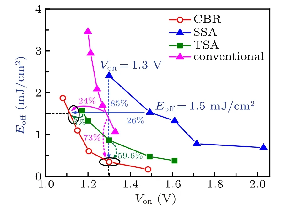
Figure 10 shows the trade-off characteristics between Vonand Eoffof different LIGBTs. The CBR LIGBT achieves the best trade-off characteristics in all LIGBTs. At the same Vonof 1.3 V, it realizes 85%, 73%, and 59.6% reductions in Eoffcompared with that of the SSA LIGBT, convention LIGBT,and TSA LIGBT, respectively. Additionally, at the same Eoffof 1.5 mJ/cm2, the Vonof the CBR LIGBT reduces by 26%,24%,and 6%compared with that of the SSA LIGBT,conventional LIGBT and TSA LIGBT, respectively. Thus, the proposed device not only achieves the snapback-free characteristic, but also obtains a better trade-off characteristics between Vonand Eoff.

Fig.10. Trade-off characteristics between Von and Eoff of different LIGBTs,with Von values of different LIGBTs obtained at JA =100 A/cm2 and Eoff value calculated by varying concentration of P+anode.
3.4. Key process of CBR LIGBT
Figure 11 shows the key process of fabricating the CBR LIGBTs. The main process can be divided into 8 steps. The oxide trench can be formed simultaneously with the SOI structure as shown in Fig.11(a). In Figs. 11(b) and 11(c), the P-body, N-buffer, P+ anode, and N+ anode can be realized by using the multiple ion implantation. Then the oxide insulation layer and polysilicon are formed by deposition and etching process as shown in Figs. 11(d) and 11(e). Note that the secondary ion implantation is needed to reach the doping concentration of the polysilicon gate as shown in Fig.11(f).Finally,the excess polysilicon and insulating layer are etched and electrodes are placed.

Fig.11. Key process of fabricating CBR LIGBT, showing (a) oxide trench and SOI structure formation, (b) P-body, N-buffer, P-float, and N-float formations, (c) P+ and N+ cathode formations, P+ and N+ anode formations, (d) oxide layer formation by deposition and etching, (e) doping of the polysilicon layer,(f)secondary ion implantation to form polysilicon gate,(g)etching excess polysilicon,and(h)etching the oxide layer and place the electrode.
4. Conclusions
The controlled barrier and resistance CBR in the anode is introduced to control the Vbarrierand RSAfor the SA LIGBT by adjusting the doping of the P-float,N-float and polisilicon layer.The results show that the CBR LIGBT not only achieves the snapback-free characteristic but also obtains better tradeoff property between Vonand Eoffthan the SSA LIGBT,conventional LIGBT,and TSA LIGBT.
猜你喜欢
杂志排行
Chinese Physics B的其它文章
- Statistical potentials for 3D structure evaluation:From proteins to RNAs∗
- Identification of denatured and normal biological tissues based on compressed sensing and refined composite multi-scale fuzzy entropy during high intensity focused ultrasound treatment∗
- Folding nucleus and unfolding dynamics of protein 2GB1∗
- Quantitative coherence analysis of dual phase grating x-ray interferometry with source grating∗
- An electromagnetic view of relay time in propagation of neural signals∗
- Negative photoconductivity in low-dimensional materials∗
