黑砷磷室温太赫兹探测器
2021-02-05朱一帆王中长
董 卓,陈 捷,朱一帆,杨 洁,王中长 ,张 凯
(1. 中国科学技术大学 纳米技术与纳米仿生学院,安徽 合肥 230026;2. 中国科学院苏州纳米技术与纳米仿生研究所 国际实验室,江苏 苏州 215123;3. 上海大学 材料科学与工程学院,上海 200444;4. 中国科学院苏州纳米技术与纳米仿生研究所 纳米器件与应用重点实验室,江苏 苏州 215123;5. 新加坡国立大学 化学与生物分子工程系,新加坡 117585;6. 伊比利亚国际纳米科技实验室 葡萄牙 布拉加 4715-330)
1 Introduction
Terahertz (THz) radiation is usually defined as electromagnetic waves in the frequency range of 0.1 THz to 10THz[1]. There are abundant interactions between THz waves and matter, which leads to plenty of THz applications in fundamental research on nondestructive tests, biomedical imaging, atmospheric observation, process control, homeland security and space communications[2-4]. The development of a reliable room-temperature (RT) THz detector is of utmost importance for these THz applications. However, constrained by the low photon energy of a THz wave (a few meV) and the strong background thermal noise at RT, traditional photodetection excited by electron-hole pairs in semiconductors are not suitable for THz photons[5]. Therefore, the basic detection mechanisms of THz photodetectors at RT should be explored. During the past two decades, many different RT THz detection technologies based on distinctive physical mechanisms have been developed. Amongst them, the most important architectures presently depend on High Electron Mobility Transistors (HEMTs)[6], Schottky barrier structures[7], bolometers[8]and Field Effect Transistors (FETs)[9]. For these architectures, FET-based THz detectors have great potential for a high-performance (fast response and high-frequency operation) and cost-effective THz detector, which also can be fabricated with a standard Complementary Metal-Oxide Semiconductor (CMOS) or silicon technology[10]. To date, the photodetection of THz waves in an FET can be achieved via three main mechanisms: Plasma-Waves rectification (PW), the Photo-Thermoelectric Effect (PTE) and bolometric detection[11-13]. The PW mechanism was first proposed by Dyakonov and Shu in the 1990s[14]and can conventionally operate at RT via rectification of the plasma waves in the FET channel using the ac electromagnetic field. The bolometric process is related to the change in the FET channel’s conductivity caused by the heat of the lattice produced by photon absorption[15]. In the case of the PTE, photovoltage can be generated by a Seebeck coefficient differ-ence and a temperature gradient within the FET channel[16]. A promising route to achieve sensitive THz detection using these mechanisms relies on a combination of the excellent properties of the chosen materials and the specific device’s structure.The dominant mechanism can be tailored through the design for the materials and structures. Therefore, it is necessary to explore various materials with potentially excellent properties to use as the active channels of the FET-based THz detectors.
Recently, two-dimensional (2D) materials,such as graphene, Transition-Metal Dichal Cogenides (TMDCs), Topological Insulators (TIs), Black Phosphorus (BP) and 2D arsenic have attracted enormous interest due to their unique and extraordinary electric and optical properties[17-23]. Increasing numbers of photodetectors based on 2D materials have been reported in the past few years.2D materials are particularly promising candidates for THz photodetectors owing to their high carrier mobility, gate-tunable carrier concentration, strong light-matter interactions and plasma oscillation[24-26].For instance, graphene and BP have been applied in asymmetrical antenna-coupled FET THz detectors utilizing plasma-wave mechanisms, and maximum RT responsivities of 30V/W and 7.8V/W were obtained at 0.3 THz, respectively[15,27]. Leonardo Viti et al.[28]reported a PW THz detector based on the Bi2Te(3−x)Sexand achieved a maximum voltage responsivity of 3.0V/W via topological insulator surface states. In addition, the RT current responsivity of 10mA/W at 2.52THz was realized in the MoS2.19-based Metal-Semiconductor-Metal (MSM)structure THz detector[29]. Black arsenic-phosphorus(b-AsxP1−x), a newly discovered 2D material similar to BP, has attracted growing attention[30,31]. In contrast to graphene and other 2D materials, b-AsxP1−xhas a finite direct band gap that allows for suppressed dark currents, which are desirable for a wealth of electronic and optoelectronic devices.Meanwhile, it exhibits a tunable band gap from 0.3 eV to 0.15 eV and different optical properties by varying the chemical composition of arsenic(b-AsxP1−x, x from 0to 0.83). This energy range suggests that b-AsxP1−xcan be extended for the detection of wavelengths from 4μm to 8μm (longwavelength infrared, LWIR). Recent research on b-AsxP1−xmainly focuses on LWIR detection, while the detection of THz has not yet been applied[32-34].The tunable band gap of b-AsxP1−xcan be exploited to selectively control the detection dynamics in the active channel and achieve efficient detection of THz waves at RT.
In this work, we demonstrated efficient antenna-coupled RT THz detectors based on a mechanically exfoliated multilayer b-AsxP1−xand studied its THz response characteristics. We found that the detection mechanism of the detector can be tailored by varying the chemical composition of b-AsxP1−x,and a competitive relationship in these mechanisms was revealed. More significantly, the best response performance of the detector can be obtained when the band gap and the carrier mobility of the materials achieve an equilibrium. We fabricated b-AsxP1−xdetectors with different components (x = 0, 0.1 and 0.5) and found that the optimal response performance was obtained in the b-As0.1P0.9detector with responsivities of 28.23V/W at 0.37THz. It is worth noting that this is the first time that a THz wave is detected with a detector based on black arsenicphosphorus.
2 Experiment
2.1 Material synthesis and characterizations
The high-quality b-AsxP1−x(x values of 0, 0.1 and 0.5) crystals were synthesized by a Chemical Vapor Transport (CVT) method similar to that of our previous report[35]. A High-Resolution Transmission Electron Microscope (HRTEM) image and a Selected Area Electron Diffraction (SAED) pattern were obtained from a TEM (Tecnai G2F20S-Twin)to characterize the crystals ’ structures and qualities.The elemental composition and distribution of synthesized materials were measured using their En-ergy-Dispersive X-ray Spectroscopy (EDS) spectrum and elemental mappings were performed with a Scanning Electron Microscope (SEM, Quanta FEG 250). The Raman spectrum was taken from a micro-Raman system (LABRAM HR) with a visible laser (λ = 532nm) through a 100× objective lens. The morphology and thickness of all flakes were characterized using a combination of the results of an optical microscope (Nikon Eclipse LV100ND) and an Atomic Force Microscope(AFM, Dimension ICON). To investigate the band gaps of the b-AsxP1−x, the infrared absorption spectroscopy was taken on a Bruker Optics Fourier Transfer Infrared spectrometer (Vertex 70) integrated with a Hyperion 1 000microscope system.
2.2 Device fabrication and characterizations
The b-AsxP1−xdetectors were fabricated by adopting standard e-beam lithography techniques. The b-AsxP1−xflakes were prepared by the mechanical exfoliation method on a high resistance (ρ >20000Ωcm) intrinsic Si substrate with 285-nm SiO2. The flakes with a thickness of about 10~15 nm were chosen by observing high-contrast optical microscope images and finally confirmed by AFM.The source and drain contact patterns were defined via Electron-Beam Lithography (EBL, JEOL JBX 5 500),and then an Electron-Beam Evaporator (EBE, Ulvac Ei-5Z) was used to evaporate Cr/Au (10/70nm)films, after which they underwent a lift-off process in acetone to form the source and drain electrodes.A 70nm thick SiO2as top-gate dielectric layer was then deposited on the samples using EBL and inductively coupled plasma chemical vapor deposition (ICPCVD, Oxford Plasmalab system 100). Finally, a Cr/Au (10/70nm) layer was evaporated onto the oxide layer to form a top-gate electrode similar to the source/drain electrode. In order to avoid the oxidation of b-AsxP1−x, the time of exposure to the ambient environment was controlled to be within one hour before the dielectric layer was deposited. The electrical characteristics of the detectors were measured at RT during ambient conditions by a probe station (Cascade M150) equipped with a semiconductor parameter analyzer (Keithley 4 200).
2.3 Optoelectronic measurements
In order to investigate the THz response of the detector, a system of THz detection was established.In the system, we employ a microwave source equipped with a Schottky-barrier-diode frequency multiplier chain (VDI WR-2.2), operating in the frequency ranges 0.24~0.38 THz. The THz radiation was then collected, collimated and focused by a set of two Off-Axis Parabolic (OAP) mirrors onto the detector surface with a spot of 2mm in diameter.The power of the incident THz (Pt) at the device’s position, which was measured as a function of output frequency by a Golay cell (Tydex GC-1P),ranged between 30μW and 370μW. The photoresponse was measured in a photocurrent mode, where the source electrode was grounded, and different gate voltages were applied by a DC voltage source(Yokogawa 7651) to obtain the maximum photocurrent (Iph). The photocurrent response signal was measured at the drain electrode by means of a lownoise current preamplifier (DL1211) to amplify the photocurrent, which was followed by a lock-in amplifier (LIA, Signal Recovery 7265) with an integration time of 200ms and a signal analyzer (SR770)to record the photocurrent signal and the noise spectral density, respectively. The value of Iphcan be calculated from the signal recorded on the lock-in(LIA) through the mathematical relation Iph=2.2LIA/Gn, where Gn(107) is the gain factor and 2.2 accounts for the square wave modulation.
3 Results and discussion
The b-AsxP1−xhas an orthorhombic crystal structure (A17type structure) with a puckered honeycomb arrangement of As and P atoms. The top and side view of the crystal structure is shown in Fig. 1(a) (color online). In order to illustrate the structure and quality of the b-AsxP1−xcrystals, the b-As0.1P0.9was characterized by TEM. Fig. 1(b) gives the HRTEM image, exhibiting the orthorhombic atomic lattice fringes and the good crystallinity of the crystals. The interplanar spacing of 0.35 nm and 0.39 nm could be measured from the HRTEM, corresponding to the (100) and (01) planes of the orthorhombic structure. Fig. 1(c) displays the SAED pattern along the [011] direction, which shows the sharp and intense diffraction spots, also suggesting the highly crystalline quality of the crystals. The elemental compositions of the b-AsxP1−x(x= 0.1 and 0.5) crystals were probed by the EDS spectrum as shown in Fig. 1(d), which displays a different signal intensity for As and P, and agrees well with the elemental composition of b-As0.1P0.9and b-As0.5P0.5(the accurate elemental ratio is shown in Fig. S1 (ab), Supporting Information). Moreover, the EDS mapping of the b-AsxP1−x, insert in Fig. 1(d), indicates a uniform spatial distribution of As and P atoms in the synthesized materials.
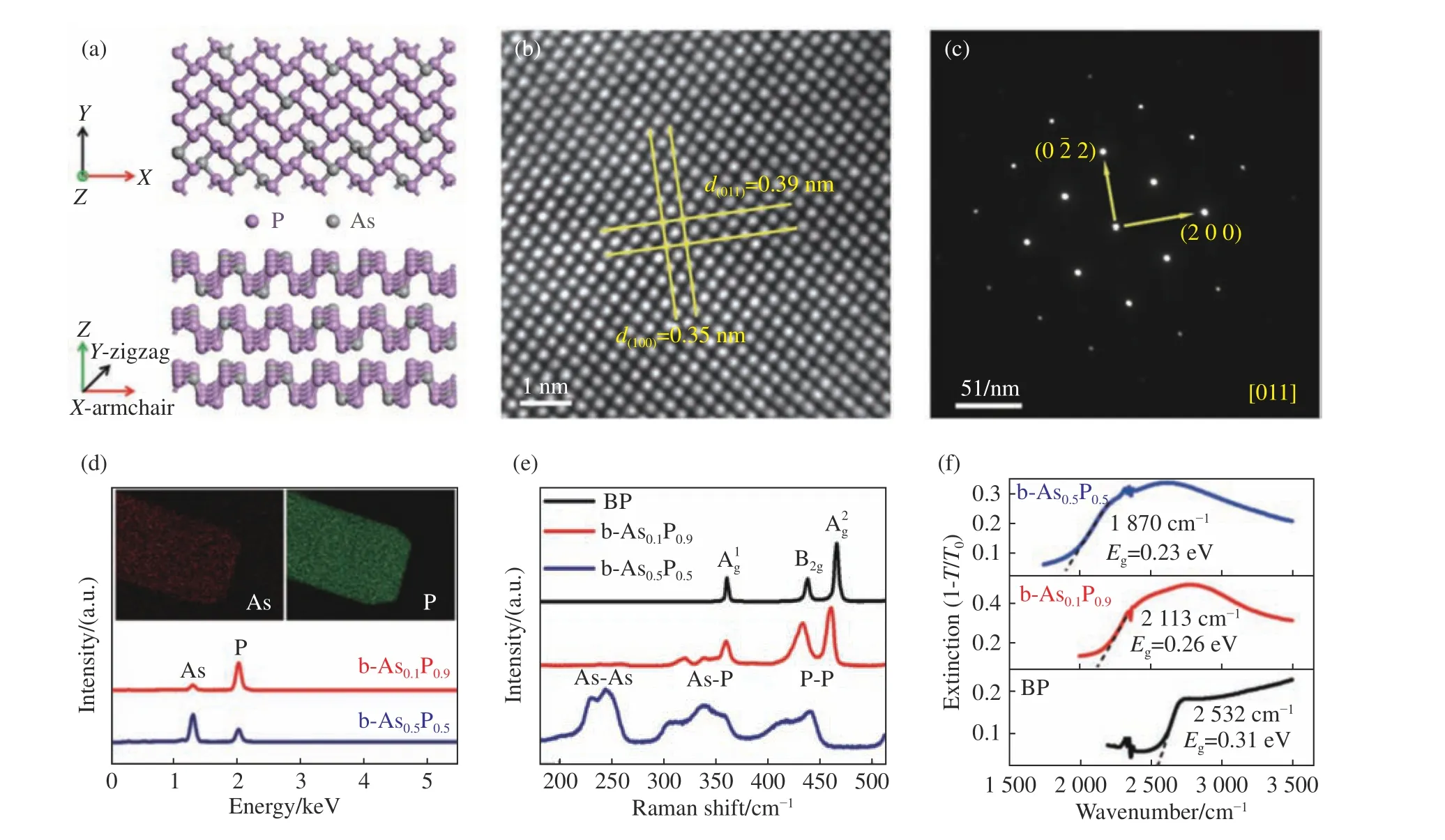
Fig. 1 (a) Top view and side view of the b-AsxP1−x crystal structure. (The armchair (X) and zigzag (Y) crystal axis are shown on the graph) (b) The HRTEM image of the b-As0.1P0.9. (c) The corresponding SAED pattern of the b-As0.1P0.9. (d)EDX result of the b-AsxP1−x (x=0.1 and 0.5) flakes, insert: EDS elemental mapping of the b-As0.1P0.9. (e) Raman spectra of b-AsxP1−x with different chemical compositions. (f) Plots of infrared absorption of different b-AsxP1−x samples
The Raman spectroscopy measurements of a few layered b-AsxP1−xand BP samples are shown in Fig. 1(e). It is obvious that the Raman spectra of BP present three characteristic peaks at 362, 438, and 466 cm−1, corresponding to the A1g, B2gand A2gphonon modes. However, b-AsxP1−xshow more Raman peaks than BP, due to the existence of As-As, As-P and P-P bands. We observed that the As-As, As-P and P-P Raman peaks are located in the 200~280cm−1, 280~380cm−1, 380~500cm−1regions, respectively. It can be seen that the relative intensity of the P-P peaks decreases, while the As-P and As-As peaks increase with an increase in the concentration of As, which agrees with previous reports[30-31].It proves the high quality of the b-AsxP1−xmaterials and that they are free of obvious damage after exfoliation. One major advantage of the b-AsxP1−xmaterials is that the band gaps can be tuned by their chemical compositions. To investigate the band gaps of our synthesized materials, the infrared ab-sorption spectra of b-AsxP1−xwith varying x values of 0, 0.1 and 0.5 were measured, as shown in Fig. 1(f). The results show a clear shift in the absorption edge to shorter wavenumbers with increasing x in b-AsxP1−xmaterials. The BP has an absorption edge of ~2532cm−1(0.31 eV), and the b-As0.1P0.9and b-As0.5P0.5have absorption edges of~2113 cm−1(0.26 eV) and ~1870cm−1(0.23 eV),respectively. Those results confirm that the band gaps change with the chemical composition of our synthesized b-AsxP1−xmaterials.
To explore the THz response properties of b-AsxP1−x, antenna-coupled FET detectors were fabricated. In order to induce the strongly localized THz fields in the active channel, the bow-tie antenna was chosen. Fig. 2(a) displays the schema of the device. It can be seen that the detector consists of three block antennas, each block is of a dipole antenna. The antenna length L = 139μm, which determines the center response frequency of 0.34 THz.To investigate the THz response of the detector, a system of THz detection was established. The schematic diagram of this system is shown in Fig. 2(b). We employed a Finite-Difference Time-Domain (FDTD) method to simulate the spatial distribution of the THz electric field for the antenna structure. The corresponding field distribution was plotted on a 2D color scale image as shown in Fig. 2(c) (color online). The THz electric field is strongly distributed at the edge of the gated channel and the THz field on the drain side is stronger than that on the source side. This proved that the antenna can achieve the asymmetric feeding of the ac field into the channel, and finally resulted in a photocurrent signal in the active channel. The detectors were then fabricated on b-AsxP1−xflakes with thickness of~15 nm, then prepared onto the Si/SiO2substrate by the mechanical exfoliation method (the AFM images are shown in Fig. S1 (c-d), Supporting Information). The S-antenna, D-antenna and G-antenna were defined with a combination of EBL and EBE(for more details see the Experimental Section), and also acted as the source, drain and gate electrodes of the FET detector, respectively. In this configuration,a 70nm thick SiO2was deposited as the dielectric layer to modulate the carrier concentration of the channel. Fig. 2(d-e) shows the false-color SEM images of the device structure. Its channel length is LC= 2.5μm, its gate length has been set to LG= 500nm and its channel width is W = 4μm.

Fig. 2(a) Schematic diagram of the b-AsxP1−x detector, including the measurement circuit. (b) Schematic diagram of the measurement system. (c) Spatial distributions of the field enhancement factors for the THz antenna. (d, e) False-color SEM image of the b-AsxP1−x detector
Before the optical testing, the RT electrical properties of the as-fabricated b-AsxP1−xdetectors were measured by the Keithley 4 200. Fig.3(a) and 3(c) display the output characteristics with different top-gate voltages (VG, ranging from −6 to 6V with steps of 3V) for the b-As0.1P0.9and b-As0.5P0.5detectors, respectively. It shows a linear relationship between the source-drain current (IDS) and sourcedrain voltage (VDS) at the differentVG, indicating good Ohmic contact between the b-AsxP1−xflakes and the metal electrodes. Furthermore, the transfer characteristics with a fixedVDS(50mV) are presented in Fig.3(b) and 3(d), exhibiting typical p-type transport behavior.

Fig. 3 (a, c) Output characteristics of the b-As0.1P0.9 detector (a) and b-As0.5P0.5 detector (c), with VG ranging from −6V to 6V with steps of 3V. Transfer characteristics for the b-As0.1P0.9 detector (b) and the b-As0.5P0.5 detector (d) with a fixed VDS = 50mV
The field-effect hole mobility of the b-AsxP1−xdevice can be calculated by the following equation:
whereLandWare the channel length and width, respectively, andCOX= 4.9×10⁻⁴F/m2is the capacitance of the 70-nm SiO2dielectric. The field-effect hole mobilities are ~159 cm2/(V·s) and 79 cm2/(V·s)for the b-As0.1P0.9and b-As0.5P0.5detectors, respectively, which were calculated from the transfer characteristics curves. For contrast, the output and transfer characteristics of the BP devices were also measured as shown in Figure S2(Supporting Information), which shows the field-effect hole mobility to be ~725 cm2/V·s.
The photoresponsivity of the as-fabricated b-AsxP1−xdetectors were characterized by illuminating the detectors using a tunable THz source with a spectral range of 0.24 THz to 0.38 THz (more details see the Experimental Section), as shown in Fig. 4. The voltage responsivity (RV) of the detector can be extracted fromIphvia the relationRV=Iph·R/(Pt·Sd/Sb), whereRis the resistance of the detector measured by the Keithley 4 200,Sbis the THz beam spot area (Sb= πr2, where r is the radius of the beam spot) and Sdis the detector’s active area. The whole area of the 139-μm antenna is smaller than that of the diffraction-limited one (Sλ), hence we assume the Sd= Sλ= λ2/4 (where λ is the wavelength of the incident THz wave). The incident radiation frequency dependence of the RVis measured at VG=0V and is shown in Fig. 4(a) and Fig. 4(c) for b-As0.1P0.9and b-As0.5P0.5, respectively. In order to obtain maximum responsivity, the source electricfield polarization must be parallel to the antenna’s axis. As shown, the RVis a function of the frequency and has several clear response peaks for all

Fig. 4 Frequency dependence of the responsivity for the b-As0.1P0.9 detector (a) and b-As0.5P0.5 detector (c), measured at VG =0V. Gate bias dependence of the responsivity for the b-As0.1P0.9 detector (b) and the b-As0.5P0.5 detector (d), measured at the optimal frequency as obtained from (a) and (c), respectively
curves, indicating the broadband nature of the bowtie antenna. Fig. 4 (b) plots the RVas a function of the VGat 0.37THz (the optimal frequency was selected from Fig. 4(a)) in the b-As0.1P0.9detector with a maximum RV= 28.23V/W while VG= −2.96V.Meanwhile, the VGdependence of the RVat 0.34 THz (selected from Fig. 4(c)) for the b-As0.5P0.5detector is shown in Fig. 4(d). The maximum RV= 2.42V/W at VG= 4.13V was obtained from the curve. For comparison, the THz response of the BP detector was measured, and the maximum RVwas found to be about 8.1V/W at 0.27THz.
The detection mechanisms can be explained by the self-mixing theory, similar to previous reports[9].The schematic diagram of the detector based on this mechanism is shown in Fig. 5 (a). The mechanism is identical to the PW mechanism. The oscillating electric field of incoming THz radiation is coupled asymmetrically between the source and gate electrodes via the bow-tie antenna, which excites plasma-waves oscillations, which in turn generate a horizontal (Ex) and vertical (Ez) driving electric field with a phase difference (φ) in the FET channel.Moreover, the driving electric field produces a modulation of drift velocity and carrier density, resulting in a mixing photocurrent (Iph).

Fig. 5 (a) Schema of the detector based on the self-mixing theory. (b) Photo-excitation and relaxation processes of the carriers in the b-AsxP1−x flakes irradiated by terahertz photons and the schematic diagram of the MSM structure based on EIW theory
The responsivity can be expressed as[36]:

which is related to the detector’s structure (antenna geometry) and the material’s characteristics (carrier mobilityμ). In our experiment, all of the detectors have the same antenna structure and fabrication process, so theRVshould be related to the channel’s conductivity with respect toVG: 1/σ·dσ/dVG(the curves are shown in Fig.S4 (a-b)). The electrical properties of b-AsxP1−xshow that the hole mobility decreases from 725 cm2/V·s (for BP detector) to 79 cm2/V·s (for b-As0.5P0.5detector). Therefore, theRVshould decrease with an increase in the concentration of As atoms. We note that theRVdid increase first and then decrease with an increase in the concentration of As atoms, and the maximumRVwas obtained in the b-As0.1P0.9detector, which is not consistent with our expectations of the mechanism.There should be a contrary effect in this detection process. Because the b-AsxP1−xis a narrow gap semiconductor, and the detector is based on a metalsemiconductor-metal structure, the Electromagnetic Induced Well (EIW) theory must also be considered[5,37], as shown in Fig. 5 (b). There is a well induced by the THz field that traps the carriers and changes the conductivity of the semiconductor to achieve THz detection. The EIW theory is related to the band gap (Eg) of the semiconductor, due to the relationship between the change of carrier concentration andEg: Δn(Δh)∝exp(-Eg/kT)[38], indicating that the smallerEgcan induce a higher fluctuation in carrier concentration. For our experiment,the higher the concentration of As atoms, the smaller theEgof b-AsxP1−x, but the lower the field-effect hole mobility. This means that it should be able to compromise for those two parameters. The characterization results of the materials and detectors show that the b-As0.1P0.9has a narrowerEg(~0.3 eV) than BP and higher mobility (~159 cm2/V·s) than b-As0.5P0.5. It ensures an ideal trade-off between the mobility and the carrier concentration fluctuation, so the b-As0.1P0.9detector displays a higherRVat 28.23V/W than the BP and b-As0.5P0.5detectors.
Another important parameter to estimate the sensitivity of the THz detector is the Noise-Equivalent Power (NEP), which is usually defined as the minimum detectable power of a detector with a unitary signal-to-noise ratio in a 1 Hz bandwidth[39]. The value of the NEP can be calculated from the voltage noise spectral density (NV) andRVvia the mathematical relationshipNEP=NV/RV. The main noiseNVis dominated by the thermal Johnson-Nyquist noise due to our device having a zero bias under optoelectronic testing. TheNVwas measured by a signal analyzer, as shown in the inset of Fig. 6(a) and 6(b)(for more details see the Experimental Section).Fig. 6(a)−(b) plots the measured NEP as a function ofVG, minimum NEP ’s of 0.53 nW/Hz1/2and 2.61 nW/Hz1/2have been attained with the b-As0.1P0.9and b-As0.5P0.5detectors, respectively. It should be noted that these values are an upper limit, because we assume that all of power incident on the antenna is coupled to the detector channel, not taking into account the coupling losses related to the impedance match.

Fig. 6 NEP as a function of the gate voltage for b-As0.1P0.9 detector(a) and b-As0.5P0.5 detector (b), insert: NV as a function of the VG. Transmission images of a key (c) and a pair of metal scissors (d) inside an envelope by the b-As0.1P0.9 detector at 0.37THz
Finally, the terahertz transmission images were obtained with a single-pixel b-As0.1P0.9detector at 0.37THz, as shown in Fig. 6(c)−(d). As the test objects, we selected a key and a pair of metal scissors inside an envelope, respectively. Fig. 6(c) shows the terahertz image of the key, consisting of 80×40 scanned points and the step size was 1mm×1mm. To minimize the noise and obtain the optimal image,the detected signal was interpreted via a lock-in amplifier with an integration time of 200ms similar to the optoelectronic test. The shape of the key is clearly revealed, with a reasonably good spatial resolution (1 mm2). The transmission image of the scissors with a total of 70×90pixels is also exhibited in Fig. 6(d), allowing us to find the concealed threats and implement security checks. These results show that our detector can be exploited in a realistic situation, enabling large-area imaging of macroscopic samples.
4 Conclusions
In conclusion, we demonstrated a RT THz photodetector based on exfoliated flakes of b-AsxP1−x(x= 0, 0.1 and 0.5) for the first time. The tunable band gap and transport characteristics of b-AsxP1−xenables efficient control of the detection mechanisms in the detector. In the experiment, the PW theory and EIW theory were found to be the primary source of the THz response signal, and there is a competitive relationship between them. We found that the PW and EIW theory are related to the carrier mobility and band gap, respectively, and the b-As0.1P0.9possesses an ideal equilibrium between the two parameters. The optimal response performance was realized in the b-As0.1P0.9detector, which shows a maximumRVof 28.23V/W and a minimum NEP of 0.53 nW/Hz1/2at 0.37THz. This work implies that b-AsxP1−xhas great potential for THz photodetector due to its tunable electronic and optical properties as well as its promising THz response performance.
Acknowledgements
This work was supported by the National Natural Science Foundation of China (Grant No. 61927 813, 61875223, 61922082) and the National Key R&D Program of China (2016YFE015700). The support from the Vacuum Interconnected Nanotech Workstation (Nano-X) of the Suzhou Institute of Nano-tech and Nano-bionics (SINANO), Chinese Academy of Sciences is also acknowledged.
Supporting Information
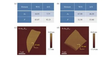
Fig. S1 (a, b) Atomic ratio of As and P elements for the b-As0.1P0.9 and b-As0.5P0.5, respectively. It proves the b-As0.1P0.9 and b-As0.5P0.5 have an accurate elemental ratio of about 1:9 and 5:5. (c, d) The AFM images of few-layer b-As0.1P0.9 and b-As0.5P0.5 nanoflakes on a Si substrate with 285 nm SiO2. It shows clean surface and flat shape, proving the high quality of the mateials. And the corresponding linear scan analysis of height display in the images with a thickness of 14 nm and 16 nm for b-As0.1P0.9 and b-As0.5P0.5 nanoflakes, respectively.

Fig. S2The electrical properties of the as-fabricated BP detector. (a) Output characteristics of the BP detector as function of different VG from −8V to 8V with steps of 4V. It shows a good Ohmic contact and a large tunable of carrier density by gate voltage. (b) Transfer characteristics for the BP detector with a fixed VDS=100mV. It exhibits a typical p-type ambipolar transport behavior. The field-effect hole mobility measured from the transfer curve is about 725 cm2/V·s.

Fig. S3 The terahertz response characteristics of the same BP detector. (a) Frequency dependence of the voltage responsivityfor BP detector at VG = 0V. It shows several clear response peaks for the detector and the maximum voltage responsivity located at 0.27THz.(b, c)Voltage responsivity and noise equivalent power as a function of the gate voltage at 0.27THz. The maximum RV and minimum NEP of about 8.1V/W and 1.08 nW/Hz1/2 were measured from the curve,respectively.

Fig. S4 Derivative of conductivity multiplied by the resistance, as a function of VG, in b-As0.1P0.9(a) and b-As0.5P0.5 (b) detector. This is the expected responsivity following a plasma-wave detection mechanism. If the domain mechanism is the PW mechanism, the measured shape of the RV curve should be in excellent agreement with that curves.