Optical properties of several ternary nanostructures*
2021-01-21XiaoLongTang唐小龙XinLuCheng程新路HuaLiangCao曹华亮andHuaDongZeng曾华东
Xiao-Long Tang(唐小龙), Xin-Lu Cheng(程新路), Hua-Liang Cao(曹华亮), and Hua-Dong Zeng(曾华东)
Institute of Atomic and Molecular Physics,Sichuan University,Chengdu 610065,China
Keywords: optical properties of nanostructures, plasmons on surfaces and interfaces, model and numerical simulation
1. Introduction
The optical properties in visible range of nanoparticles have been widely studied,[1–4]especially for TiO2and Au.[5–7]As a crucial material in photocatalysis, TiO2has received extensive attention since Fujishima and Honda demonstrated that TiO2can be used for photocatalysis in 1972.[8]However,the photocatalytic efficiency of TiO2is insufficient for photocatalytic applications. To improve the photocatalytic efficiency,TiO2was coupled with noble metal nanoparticles,[9,10]such as Au,[11]Ag,[12]Cu,[13]Pt,[14]etc. Meanwhile, noble metals have strong ability to transfer electrons, making the separation efficiency of electrons and holes higher,thus increasing the catalytic ability of materials.[15,16]Noble metals were also coupled to many materials to obtain different properties,[17,18]such as Fe3O4–Au (Ag),[19]ZnO–Au(Ag),[20]SiO2–Au(Ag),[21]ZrO2–Au,[22]TiO2–Au(Ag),[23]etc. As an efficiency combination, Janus TiO2–Au nanostructure has attracted more and more interest in photocatalysis. Seh et al. first demonstrated that TiO2–Au asymmetric Janus nanoparticleis possess higher efficiency to generate hydrogen than bare Au and core–shell structure in visible-light photocatalysis.[24]Wang et al. investigated the photocatalyst properties of Au/TiO2/Au nanostructure which exhibits a significant improvement in photocurrent density compared with the bare TiO2nanostructure in visible range.[25]Li and Li reported that an Au/Au3+TiO2photocatalyst can not only extend the light absorption of TiO2-based photocatalyst into visible range but also eliminate the rapid recombination of excited electrons/holes during photoreaction.[26]However, for Au–TiO2nanostructure, TiO2with a wide band gap width of 3.2 eV can provide energetic electrons for photocatalysis but lacks extinction in visible range. Au can excite the extinction of TiO2in visible range, but cannot extend the extinction range. Thus this combination of Au and TiO2possesses an improvement in the light absorption but a narrow extinction range in visible light. This restricts the utilization of visible light which contains the majority of the energy of sun light. Therefore, extending the light extinction range in visible light is vital for photocatalysis of Au and TiO2. Some investigations indicated that narrow band gap materials can sensitize wide band gap materials in visible light.[1–3]Therefore,finding a suitable and applicable material combined with TiO2and Au is a feasible way to improve photocatalysis in visible light.[27,28]Ma et al.[29]and Tada et al.[30]found that the CdS–Au–TiO2three-component nanojunction system exhibits much more photocatalytic activity than single-and twocomponent system. However, most of structures consisting of multiple components are of core–shell or multiple sphere.The core–shell structure can provide a huge interface between different materials, but the incident light cannot radiate inner materials directly,thereby limiting the interaction between materials under the incident irradiation.[31]Multiple-sphere structure can be illuminated directly by the incident light,but the interface between the spheres is very small, which also limits the interaction between materials. With the development of micro-nanometer manufacturing technology, Janus nanodisk has been fabricated,[32]and it is possible to generate the ternary nanodisk. In this structure,three materials are illuminated by the incident light directly,and there is a considerable interface between each two materials.
In this paper, several ternary nanostructures , each with three equal volume parts, are designed. We calculate the optical properties of several types of ternary nanostructures by the the discrete dipole approximation(DDA)method,and the mechanism of the interaction among three materials is discussed.
2. Method
Since Mie calculated the nanospheres of Au by solving Maxwell’s equations,[33]more and more complex and different nanoparticles have been calculated. Benefiting from the fantastic work of Draine[34]and Draine and Flatau,[35]DDSCAT7.3[36]was used to simulate different kinds of nanostructures. DDSCAT is an efficient,open-source and free software package which is based on the theory of DDA. In the DDA method,the object is regarded as N-dipoles and the polarizations of these dipoles are calculated to simulate different materials with arbitrary morphologies and sizes.It can be used to calculate the extinction coefficients and near-field intensities of these nanoparticles.
The real V is divided into N dipoles,and each dipole possesses volume d3in this soft package,specifically,


In the simulation, the more the dipoles used, the more accurate the calculation is. Previous work shows a relative accuracy when N 1000.[37,38]In our calculations 157200 dipoles are used to simulate the nanostructure in order to obtain relatively high accurate results.The wavelengths we discussed are all between 300 nm and 750 nm. More computational details can be found in the reference.

Fig.1. Morphology of(a)ternary core–shell,(b)nanodisk,and(c)three-sphere structure.
The morphology of the ternary core–shell, nanodisk and three-sphere structures are presented in Fig.1. The core–shell structure is a three-layer sphere structure,with outer layer radius being R3,the core radius R1,and the meddle layer radius R2, the three parts possess equal volume(Fig. 1(a)). In addition, the morphology of the core–shell structure in Fig. 1 is the cross-section diagram of this structure, and the real morphology in calculation of the structure is a complete core–shell structure. The radius of the nanodisk is R, and the thickness is d (Fig. 1(b)). The nanodisk is divided into three parts,M1=M2=M3=1/3 nanodisk. The three-sphere structure is composed of three spheres of equal radius R1. M1,M2,M3are three different materials (Fig. 1(c)). The incident light is linear radiation propagating along the ˆxLFaxis. The polarization direction is parallel to ˆzLF.[39]The ambient medium is set to be vacuum where the refractive index is 1.
3. Results and discussion
The surface plasmon resonance of nanoparticles is dependent on geometry,size,material composition and surrounding medium.[40–43]Among these factors,the geometry and material composition are the key points for studying the surface plasmon resonance of nanoparticles. A kind of ternary nanostructure composed of three different materials is designed and the optical properties are investigated in this work.
For ternary nanostructures, the core–shell and threesphere structures are widely studied,[44,45]but the nanodisk structure is less concerned. To investigate the optical properties of ternary nanostructures,the extinction spectra of nanodisk, core–shell and three-sphere structures with equal volume of TiO2, Ag, and Au are calculated, in which the nanodisk structure is M1/M2/M3=TiO2/Ag/Au, the radius R of the nanodisk is 50 nm,and the thickness d is 20 nm. And the core–shell structure is of a three-layer sphere, which is composed of the core sphere, middle shell, and outer shell. The core sphere is of Ag with radius R1of 23.21 nm, the middle shell is of TiO2with a thickness of 6.04 nm,and the outer shell is of Au with a thickness of 4.23 nm. The three-sphere structure is composed of three spheres with a radius R1is 23.21 nm,which contact each other. They are composed of three spheres of TiO2, Au, and Ag. The extinction spectrum of nanodisk,core–shell and three-sphere structures are shown in Fig. 2.The extinction properties of nanodisk structure are much better than those of the core–shell structure and three-sphere structure in 300 nm–750 nm. This is due to the interaction among materials and the migration of electrons needing enough energy(incident light)and touching area(interface). The core–shell structure has a large interface among materials, but the incident light cannot directly irradiate the internal materials,which greatly reduces the interaction between the materials.In the three-sphere structure, although the incident light can directly irradiate the three materials, the interface among the three materials is less, also limiting the interaction between the materials. In the nanodisk structure,the incident light can directly irradiate three materials, and there is a considerable interface,so the interaction among materials is promoted.
Several researches show that narrow band gap materials can sensitize the extinction characteristics of TiO2in the visible light range.[2,46]In order to study the sensitization effect of narrow band gap materials on TiO2under the local surface plasmon resonance excitation of Au,the extinction spectra of the nanodisk consiting of different band gap materials combined with Au and TiO2are calculated and discussed. We select a series of band gap materials to combine with TiO2[47]and Au.[48]The band gap width of these materials possess an approximately equal difference, PbSe (0.165 eV),[49]Ge(0.66 eV),[50]MoS2(1.17 eV),[51]CdSe(1.7 eV),[52]and CdS(2.4 eV).[53]

Fig.2. Extinction spectrum of core–shell,nanodisk,and three-sphere structures for M1/M2/M3=TiO2/Ag/Au.

Fig. 3. Extinction spectra of M1/M2/M3 structures, with M1 fixed to Au,M2=M3 being PbSe,Ge,MoS2,CdSe,CdS or TiO2 respectively.
For M1=Au, M2=M3=PbSe, Ge, MoS2, CdSe, CdS or TiO2respectively,the extinction spectra of nanodisk structures are shown in Fig.3. By analyzing the band gap width of M2and M3(PbSe=0.165 eV,Ge=0.66 eV,MoS2=1.17 eV,CdSe=1.7 eV, CdS=2.4 eV), the results show that the extinction coefficient is inversely proportional to the band gap for each of M2and M3in 300 nm–600 nm. The narrow band gap width leads to the low electronic transition energy and the high carrier concentration in equilibrium state. Therefore,under the excitation of the near-field energy generated by the local surface plasmon resonance of Au, the valence band electrons are more likely to be excited and transited to the conduction band in narrow band gap material, as a result, the absorption rate and extinction coefficient are both high. At the same time, when M2=M3=PbSe, Ge or MoS2, there is no extinction peak in 600 nm–700 nm, but there is an extinction peak at 676 nm, 652 nm or 658 nm respectively for M2=M3=CdSe,CdS or TiO2. This is due to the strong coupling between the plasmonic near-field produced by Au and the electronic transition energy in semiconductor. The electrons transit from valence band to conduction band under the excitation of plasmonic near-field,and the electron–hole pairs are formed. Since the Fermi energy level of semiconductor is higher than that of metal, when the two materials contact each other,the excited electrons will flow from semiconductor with high Fermi energy level to noble metal with low Fermi energy level,until their Fermi energy levels become the same and reach a static equilibrium. Due to the narrow band gap width of PbSe,Ge and MoS2,the energy values of the transition electrons from the bands are too low to pass through the Schottky barrier between Au and the material.[54–56]It cannot form a path to transfer the electrons from material to Au.[57]The band gap width of CdS, CdSe, and TiO2are wide. The transition electrons generated in CdS, CdSe, and TiO2have enough energy to pass through the Schottky barrier between the material and Au, and flow into Au until their Fermi energy levels reach a balance state, which effectively promotes the charge separation in semiconductor. In this process, the electron–hole pairs produced by electron transition and transfer can produce redox reaction with surrounding oxidants and reducers,thereby completing photocatalysis.
From the above structures, the M1/M2/M3=Au/PbSe/PbSe structure has the maximum extinction coefficient in 300 nm–600 nm,and the M1/M/M3=Au/TiO2/TiO2structure has a maximum extinction coefficient in 600 nm–750 nm. Based on above results,to investigate how the different materials combined with Au and TiO2structure influence the extinction coefficient,the extinction spectra of the ternary nanodisk structures are calculated.

Fig.4. Extinction spectra of M1/M2/M3 nanodisk structures with M1 =Au and M3=TiO2,and M2=PbSe,Ge,MoS2,CdSe or CdS respectively.
The extinction spectra of the ternary nanodisks composed of Au, a semiconductor (PbSe, Ge, MoS2, CdSe or CdS)and TiO2are shown in Fig. 4. The extinction coefficient of M1/M2/M3= Au/PbSe/TiO2structure is always highest in 300 nm–600 nm. In 600 nm–750 nm, the extinction coefficient peak of M1/M2/M3= Au/CdS/TiO2structure is the highest, but the difference in extinction peak between different structures is small. The results show that the structure of M1/M2/M3=Au/PbSe/TiO2has the best extinction performance in the whole range of 300 nm–750 nm. Similarly, the extinction coefficient of the structure is also inversely proportional to the band gap width of M2material in 300 nm–600 nm.Because M1and M3are the same in each structure,the difference is mainly caused by M2material. The band gap width of M2material directly affects the extinction coefficient of this type of structure.
Figures 5(a)–5(e) show the electric near-field distributions of the two different semiconductors and Au ternary nanodisks at 530 nm.The electric near-field distribution is consistent with the results of above extinction spectra.The near-field intensity outside the M2material is also inversely proportional to the band gap width of the M2material.This is because under the plasmonic near-field excitation,the smaller band gap leads the greater carrier concentration and the smaller transition energy,which makes the occurrence probability of the transition greater,so the absorption is greater. The boundaries of PbSe,Ge, and MoS2are very clear in Fig. 6, and the electric nearfield distributions in the three materials are all small. Due to the fact that at the interface between Au and these materials there exists a Schottky barrier while the transition electrons of these materials are not energetic enough to pass through the Schottky barrier, the electron–hole pairs formed in the material recombine rapidly,which prevents the electron–hole pairs from being continuously produced, leading the internal electric near-field distribution to become small.However,there are some near-field distributions near the interface of CdSe,CdS,TiO2, and Au, indicating that the transition electrons generated in these materials are energetic to cross the Schottky barrier between them and Au, thus further promoting the electrons’ transition and light absorption. The above-mentioned electric near-field distribution verifies the previous Schottky barrier theory discussed in extinction spectra.
Figures 6(a)–6(e) show the electric near-field distributions of the ternary nanodisks, each of which is composed of two semiconductors and Au for the second peak in 650 nm–690 nm. There are a large number of near-field distributions around the interface between Au and TiO2at the maximum extinction peak,which is due to the strong coupling between the electronic transition in TiO2and the plasmonic near-field of Au.Because of the difference in Fermi energy level,the Fermi energy level of TiO2is higher than that of Au. A large number of electrons from the valence band in TiO2are injected into Au,which slows down the electron–hole pairs recombining in TiO2. It further enhances the efficiency of charge separation in TiO2, until the Fermi energy level of TiO2and Au reach a static balance. Therefore,a strong electric near-field distribution is produced near the interface between TiO2and Au. like the electric near-field distribution near 530 nm,the boundaries of PbSe,Ge,MoS2materials are also very clear for the same reason.
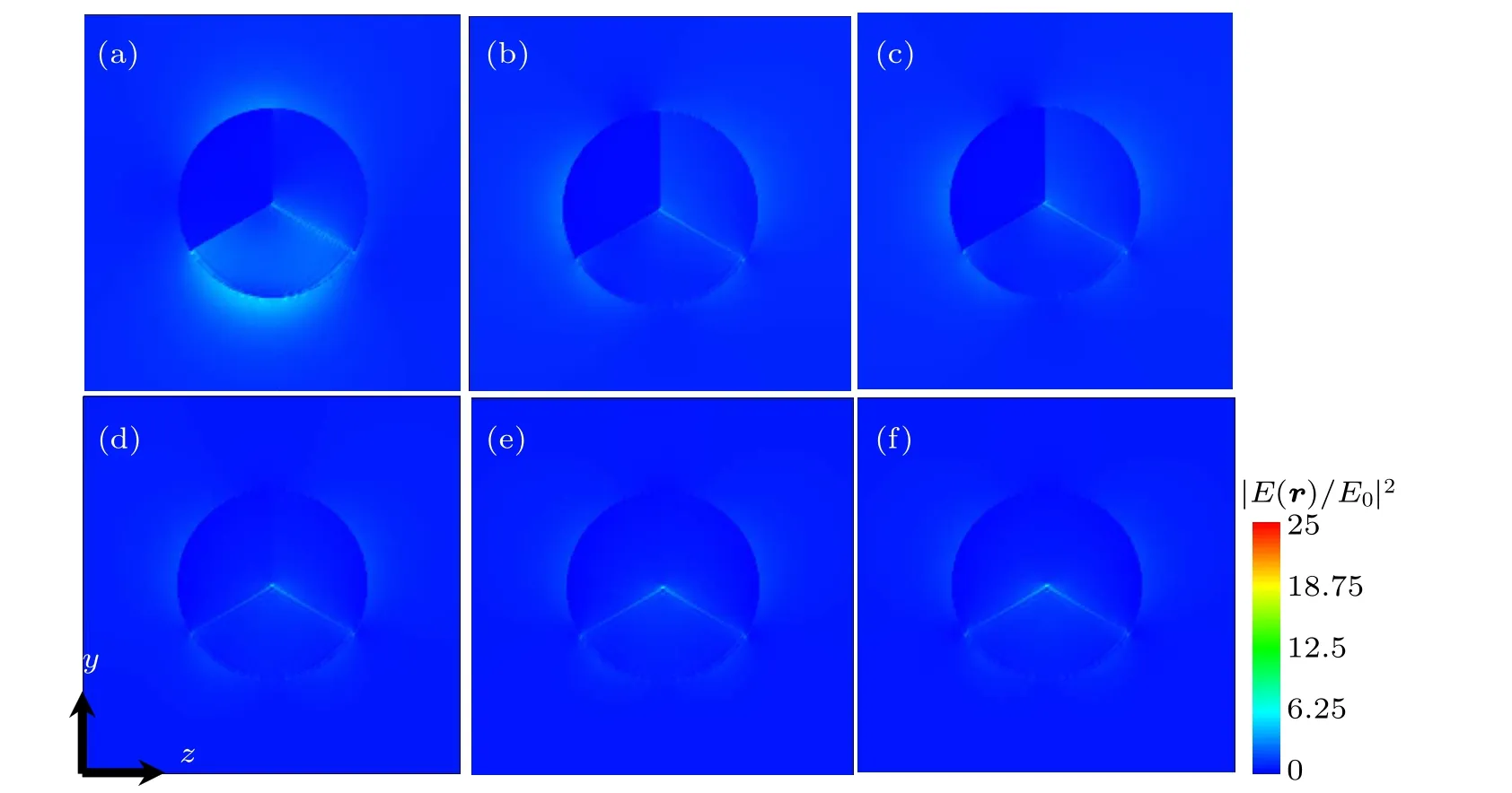
Fig. 5. Electric near-field distribution maps of the peaks at 530 nm for (a) M1/M2/M3 =Au/PbSe/TiO2, (b) Au/Ge/TiO2, (c) Au/MoS2/TiO2, (d)Au/CdSe/TiO2,(e)Au/CdS/TiO2,and(f)Au/TiO2/TiO2 structures in x plane.
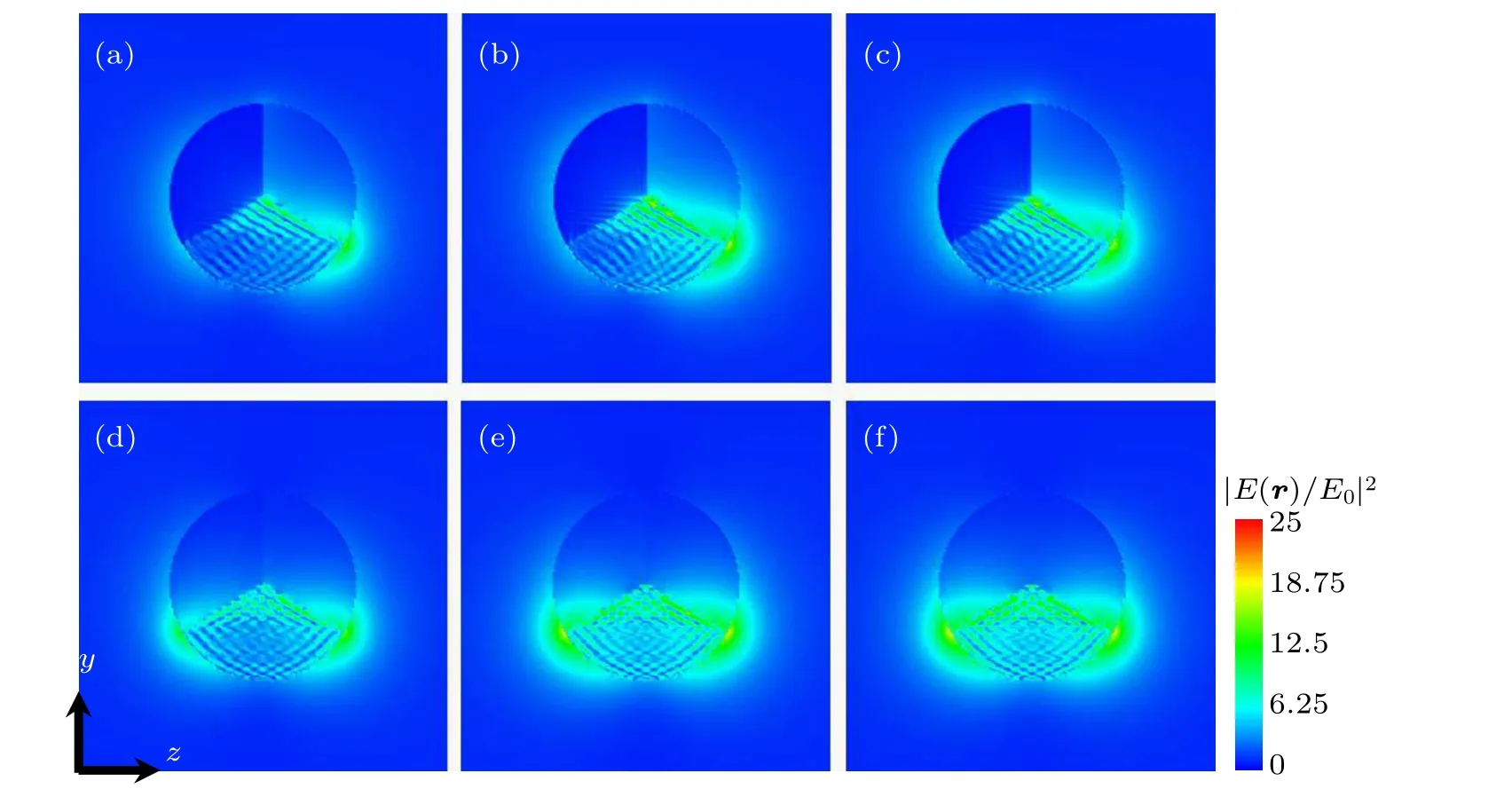
Fig.6. Electric near-field distribute maps of the second peak between 650 nm and 690 nm for(a)M1/M2/M3 =Au/PbSe/TiO2, (b)Au/Ge/TiO2, (c)Au/MoS2/TiO2,(d)Au/CdSe/TiO2 (e)Au/CdS/TiO2,and(f)Au/TiO2/TiO2 in x plane.
The extinction spectrum of the ternary nanodisk consisting of two different noble metals and TiO2is calculated. Figure 7 shows the extinction coefficient spectrum of M1/M2/M3=TiO2/Ag/Au,TiO2/Ag/Pt and TiO2/Au/Pt structures. The results show that the M1/M2/M3= TiO2/Ag/Pt structure has the best extinction performance in 300 nm–750 nm. The M1/M2/M3= TiO2/Ag/Au structure has two absorption peaks at 406 nm and 546 nm, respectively. The M1/M2/M3=TiO2/Ag/Pt structure has three extinction peaks at 410 nm, 670 nm, and 694 nm, respectively, and the M1/M2/M3=TiO2/Au/Pt has two extinction peaks at 532 nm and 732 nm, respectively. There is an extinction peak near 400 nm for structure containing Ag,540 nm for structure containing Au,and 700 nm for structure containing Pt.This is due to the fact that the coupling extinction peak of Ag and TiO2is near 400 nm, the coupling extinction peak of Au and TiO2is near 500 nm,and the coupling extinction peak of Pt and TiO2is near 700 nm.[58,59]The difference among the material combinations might be the reason for causing some differences in the location and value of extinction peaks. Based on above results,there is a complementation of extinction efficiency between the TiO2/Ag/Au and TiO2/Ag/Pt structures in visible range.
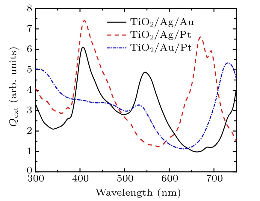
Fig. 7. Extinction coefficient spectrum of M1/M2/M3 = TiO2/Ag/Au,TiO2/Ag/Pt,and TiO2/Au/Pt structures.
The electric near-field distributions of M1/M2/M3=TiO2/Ag/Pt structure at extinction peaks of 410 nm, 670 nm,694 nm are calculated. The electric near-field distribution at 410 nm, 670 nm, and 694 nm in the x plane are shown in Figs. 8(a1), 8(b1), and 8(c1), respectively. And the electric near-field distribution in the y plane at 410 nm, 670 nm, and 694 nm are shown in Figs. 8(a2), 8(b2), and 8(c2), respectively. The electric near-field distribution at 410 nm is mainly concentrated in the part of M2=Ag. The electric near-field distribution at 670 nm is similar to that at 694 nm, which are mainly distributed around M2and M3, and the distribution is larger in M2. It is due to the fact that both Ag and Pt have a coupling effect with TiO2, resulting in two extinction peaks,and that the distance between the two coupling extinction peaks is very close,so the structure has two adjacent extinction peaks at 670 nm and 694 nm.
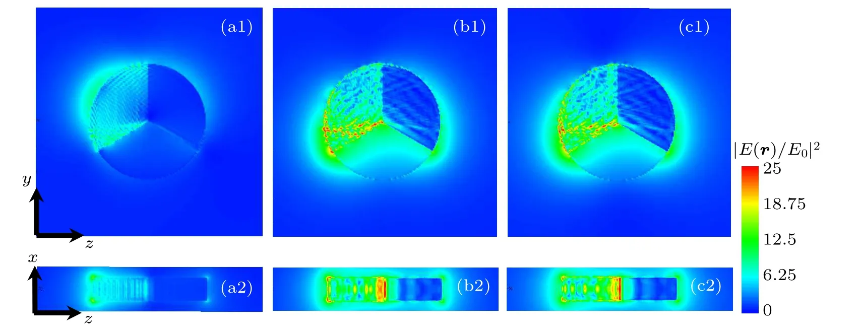
Fig.8. Near-field distribution of M1/M2/M3 =TiO2/Ag/Pt structure at(a1)410 nm, (b1)670 nm, (c1)694 nm in x plane and(a2)410 nm,(b2)670 nm,(c2)694 nm y plane.
4. Conclusions
We conclude that the ternary nanodisk has better extinction properties than core–shell and three-sphere structures.For the nanodisk structures of M1/M2/M3=Au/(PbSe, Ge,MoS2, CdSe, or CdS)/TiO2, the best extinction performance is obtained for Au/PbSe/TiO2ternary nanodisk in 300 nm–750 nm. And the extinction coefficient is inversely proportional to the band gap of M2in 300 nm–600 nm. When M1/M2/M3=TiO2/Ag/Au,TiO2/Ag/Pt or TiO2/Au/Pt of nanodisk structures,the TiO2/Ag/Pt nanodisk has the best extinction performance. The extinction efficiency and electric nearfield intensity of TiO2/Ag/Pt structure are much higher than those of Au/PbSe/TiO2. The TiO2/Ag/Pt nanodisk structure has two extinction peaks and strong electric near-field in visible range,so it is hopeful to achieve a better efficiency in the field of photocatalysis. The spectrum of TiO2/Ag/Pt structure and the spectrum of TiO2/Ag/Au structure can form a threepeak extinction spectrum in visible range, it provides a reference for extending the extinction range.
猜你喜欢
杂志排行
Chinese Physics B的其它文章
- Numerical simulation on ionic wind in circular channels*
- Interaction properties of solitons for a couple of nonlinear evolution equations
- Enhancement of multiatom non-classical correlations and quantum state transfer in atom–cavity–fiber system*
- Protein–protein docking with interface residue restraints*
- Effect of interaction between loop bases and ions on stability of G-quadruplex DNA*
- Retrieval of multiple scattering contrast from x-ray analyzer-based imaging*