TiOx-based self-rectifying memory device for crossbar WORM memory array applications*
2021-01-21LiPingFu傅丽萍XiaoQiangSong宋小强XiaoPingGao高晓平ZeWeiWu吴泽伟SiKaiChen陈思凯andYingTaoLi李颖弢
Li-Ping Fu(傅丽萍), Xiao-Qiang Song(宋小强), Xiao-Ping Gao(高晓平),Ze-Wei Wu(吴泽伟),Si-Kai Chen(陈思凯), and Ying-Tao Li(李颖弢),‡
1Key Laboratory of Special Function Materials and Structure Design,Ministry of Education,Lanzhou University,Lanzhou 730000,China
2School of Physical Science and Technology,Lanzhou University,Lanzhou 730000,China
3Key Laboratory of Sensor and Sensing Technology,Gansu Province,Lanzhou 730000,China
Keywords: resistive switching memory,write-once-read-many-times(WORM),self-rectifying,crossbar array
1. Introduction
Resistive switching (RS) memory device has been considered to be one of the most promising candidates for nextgeneration nonvolatile memories due to its simple structure,high switching speed, excellent scalability, low power consumption,high integration density,and compatibility with the current complementary metal oxide semiconductor (CMOS)technology.[1–5]As one type of RS memory device, writeonce-read-many-times (WORM) memory devices are receiving increasing interest because they are widely used in all kinds of permanent data storage applications such as archival storage equipment, secure databases, as well as electronic labels.[6–8]To achieve high storage capacity, crossbar array with the smallest cell size of 4F2is adopted. Generally,the integration of an addition selection diode to each cell is used to suppress the unexpected sneak current in crossbar structure.[8,9]Recently,the WORM memory devices with selfrectifying characteristics in low resistance state (LRS) provide a more desirable solution to suppress the sneak current without the externally added diode. However, the rectification ratios of most of the reported WORM memory devices with self-rectifying characteristics are not very high.[10,11]In previous work,a self-rectifying WORM memory device based on n+-Si/ZrO2/Pt structure with a high rectification ratio over 104was demonstrated,[12]in which highly doped crystal silicon was used as the bottom electrode. However, from threedimensional(3D)high-density integration point of view,crystal silicon is not expected.[13]
In this paper, by using tungsten (W) as the bottom electrode, we demonstrate a high-performance self-rectifying WORM memory device with a simple Pt/TiOx/W structure.After programming the fresh device to LRS by applying the voltage of -5 V, a high rectification ratio as high as 104is obtained. Such a high rectification ratio can overcome the crosstalk issue in crossbar array without extra diodes. In addition,the physical mechanism is investigated.
2. Experiments
The titanium oxide-based WORM memory devices in this study were prepared using the following processes. A 70-nmthick W bottom electrode(BE)was deposited on SiO2/Si substrate by sputtering.Subsequently,20-nm-thick titanium oxide film was deposited on the W bottom electrode by atomic layer deposition(ALD)system. TiCl4was used as the Ti precursor and H2O was used as the oxygen precursor. An atomic layer deposition cycle with 4 steps was adopted for this experiment.The 4 steps were TiCl4reactant,N2purge,H2O reactant,and N2purge,respectively. During the deposition,the temperature was maintained at 150◦C.Finally,70-nm-thick square-shaped platinum(Pt)top electrodes(TE)with areas of 100×100 μm2were deposited and defined by photolithography and lift-off process to form Pt/TiOx/W structure devices. The composition and binding energy analysis of the deposited TiOxfilm was performed using x-ray photoelectron spectroscope(XPS).The current–voltage(I–V)characteristics of the fabricated devices were measured by a Keithley 4200-SCS semiconductor characterization system at room temperature. During the measurements, the bias voltage was applied on the top electrode while the bottom electrode was grounded.
3. Results and discussion
To confirm the chemical nature and the existence of the defects in the deposited TiOxfilm, the XPS depth profiling was performed as shown in Fig.1. From XPS depth profiling,the TiOxfilm is composed of two layers(here referred to as top layer and bulk layer). The XPS spectrum of the top layer film(surface to 4 nm)in Fig.1(a)shows that O 1s peak is associated with TiO2layer indicating the stoichiometric oxide layer.In contrast,the XPS spectrum of the bulk layer film(4 nm to 20 nm) in Fig. 1(b) shows that the profile of the O 1s spectrum can be fitted by two Gaussian components at 531.0 eV and 531.9 eV. The component of the low binding energy locating at 531.0 eV is associated with the O2-ions from the Ti-O bonding, and the high binding energy locating at 531.9 eV is related to oxygen deficiencies of the TiOxlayer,[14,15]which indicates metal excess nonstoichiometric TiOxlayer of the bulk layer film.
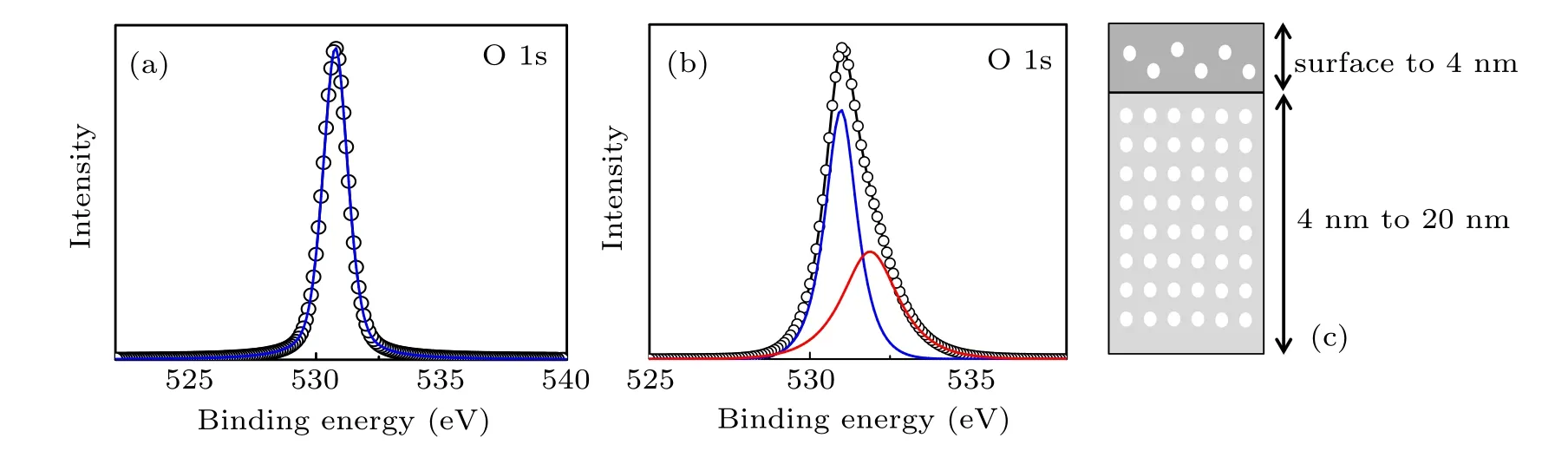
Fig.1. XPS spectra of O 1s in the deposited TiOx film. (a)Top layer film: from surface to 4 nm in depth,and(b)bulk layer film: from 4 nm to 20 nm. (c)Schematic representation of the structure of the deposited TiOx film in depth.
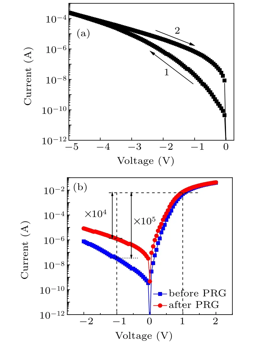
Fig. 2. (a) Programming process (PRG) of the as-deposited fresh device. (b) Typical I–V curves of the Pt/TiOx/W memory device before and after PRG.
Figure 2 shows the typical I–V curves of the Pt/TiOx/W structure device. As shown in Fig.2(a),the as-deposited fresh device is in an initial high resistance state (HRS). By sweeping the voltage from zero to a negative voltage, a gradual increase of the device current can be observed, and the device switches from the initial HRS to low resistance state(LRS)by increasing the voltage to about -5 V and then keeps in LRS permanently and steadily. Figure 2(b) shows the typical I–V curves of the Pt/TiOx/W device before and after the programming process(PRG).It can be observed that the resistance ratio between HRS and LRS exceeds 10 by using a-1 V readout voltage. More importantly,a pronounced rectifying characteristic with the rectification ratio as high as 104can be obtained after PRG. With such a self-rectifying behavior in LRS, the undesired sneak current can be suppressed, and the crosstalk issue can be avoided effectively in the crossbar array.
Although various models have been proposed to explain the resistive switching behaviors in WORM memory devices,the intrinsic mechanism is still unclear,especially for the selfrectifying WORM memory device.[10–12]Based on the XPS data shown in Figs. 1(a) and 1(b), the fabricated TiOxfilm is composed of two layers,including top stoichiometric TiO2layer with high resistance and nonstoichiometric TiOxbulk layer with more oxygen deficiencies, as schematically summarized in Fig. 1(c). Compared with the top TiO2layer, the bulk TiOxlayer shows much higher conductivity due to the existence of more oxygen deficiencies. Therefore, when a negative voltage is applied to activate the fresh memory device,the high voltage is only applied on the top high resistance layer and it causes soft-breakdown of the top high resistance layer,[16]leading to the LRS of the Pt/TiOx/W WORM memory device after the programming process. To further clarify the self-rectifying current conduction mechanism of the Pt/TiOx/W WORM memory device, the I–V curves in both HRS and LRS are analyzed using different theoretical models. As shown in Fig. 3, lnI has a linear relation to V1/2for both HRS and LRS,indicating that the resistive switching behavior of the Pt/TiOx/W WORM memory device is dominated by the Shcottky emission model.[8,12]In our previous work,it has been confirmed that the TiOx/W interface is Ohmic contact and the Pt/TiOxinterface is Shcottky contact.[17]Therefore, the electron injecting barrier at the Pt/TiOxinterface is higher than that at the TiOx/W interface, resulting in the self-rectifying resistive switching behavior in the Pt/TiOx/W WORM memory device.
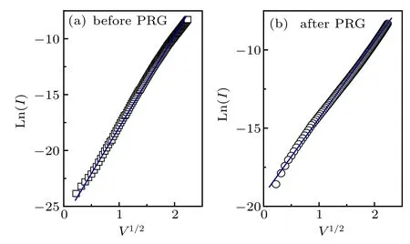
Fig. 3. Analysis of the lnI–V1/2 curves (a) before and (b) after PRG with the Shcottky emission model.
To evaluate the uniformity of the Pt/TiOx/W WORM memory device, the statistical measurements of resistances distribution of 20 randomly chosen devices in different positions of the two inches wafer were performed. Figure 4(a)shows the statistical data of the resistances obtained by±1 V read voltages before (RB) and after (RA) programming. And the mean values(μ)and standard deviations(σ)of RBand RAat-1 V and 1 V read voltages are 1.09×10⁸Ω(9.63×10⁷Ω),424 Ω(64 Ω),2.35×106Ω(8.28×10⁵Ω),and 244 Ω(34 Ω),respectively. Except for the RBat -1 V read voltage, all the other resistances exhibit narrow distributions with good uniformity. Furthermore,it can be seen from Fig.4 that the reading window margin at the -1 V read voltage excesses 10,which is large enough to distinguish these two states to store information. Furthermore, the HRS rectifying ratio higher than 105and LRS rectifying ratio as high as 104can be observed for different memory devices. The retention characteristic of the Pt/TiOx/W WORM memory device is also characterized and shown in Fig. 4(b). First, the retention test is carried out on the fresh device before PRG. Then, the same device is programmed to the LRS by applied a -5 V voltage.The resistances in both states are stable and no significant degradation is observed for over 104s,which demonstrate the nonvolatile storage capability of the Pt/TiOx/W WORM memory device.
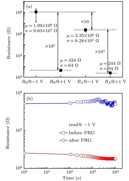
Fig. 4. Device-to-device distributions of the resistances obtained by±1 V read voltages before and after PRG. All the statistical data are obtained from 20 random devices. (b) Retention characteristic of the Pt/TiOx/W WORM memory device.
4. Conclusions
We have successfully demonstrated a self-rectifying WORM memory device with promising memory characteristics such as excellent uniformity and good retention. Moreover,a remarkable self-rectifying effect in LRS could be also observed in the device,which can minimize the crosstalk issue in the crossbar array. The Ohmic contact at TiOx/W interface and the Schottky contact at Pt/TiOxinterface are suggested to explain the self-rectifying behavior of the Pt/TiOx/W WORM memory device.
猜你喜欢
杂志排行

Chinese Physics B的其它文章
- Two-dimensional finite element mesh generation algorithm for electromagnetic field calculation*
- Stable water droplets on composite structures formed by embedded water into fully hydroxylated β-cristobalite silica*
- Surface active agents stabilize nanodroplets and enhance haze formation*
- Synchronization mechanism of clapping rhythms in mutual interacting individuals*
- Theoretical study of the hyperfine interaction constants,Land´e g-factors,and electric quadrupole moments for the low-lying states of the 61Niq+(q=11,12,14,and 15)ions*
- Ultrafast photoionization of ions and molecules by orthogonally polarized intense laser pulses: Effects of the time delay*