Effect of pressure on the electrical properties of flexible NiPc thin films fabricated by rubbing-in technology
2021-01-21KhasanKarimovFahmiMuhammadsharifZubairAhmadMuqeetRehmanandRashidAli
Khasan S Karimov, Fahmi F Muhammadsharif, Zubair Ahmad, M Muqeet Rehman, and Rashid Ali
1GIK Institute of Engineering Sciences and Technology,Topi,District Swabi,KPK,23640,Pakistan
2Center for Innovative Development of Science and New Technologies of Academy of Sciences of Tajikistan,Dushanbe,734025
3Department of Physics,Faculty of Science and Health,Koya University,44023 Koya,Kurdistan Region-F.R.,Iraq
4Center for Advanced Materials(CAM),Qatar University,P.O.Box 2713,Doha,Qatar
5Department of Electronic Engineering,Jeju National University,Jeju,Republic of Korea
Keywords: pressure,electrical property,NiPc,thin film,rubbing-in technology
1. Introduction
The emergence of organic semiconductors in electronics has made great progresses in the development of various important devices such as solar cells, diodes, transistors, memories, spin valves and sensors.[1–7]This is because organic semiconductors offer unique chemical and physical properties including optoelectronic selectivity,molecular tunability, light weight, and flexibility. Phthalocyanine (Pc) and its derivates play a splendid role in the establishment of viable electronic devices thanks to their ease of fabrication,stability, high carrier mobility, and compatibility with flexible substrates.[8–10]Having sufficient information regarding the electrical properties of organic materials is crucial before they get involved in the device application. Nickel phthalocyanine(NiPc) films have been successfully grown by dipping and spray-layer-by-layer (LbL) and the effect of deposition techniques on their electrochemical and morphological properties were investigated.[11]Tarrad et al. used thermal evaporation technique to deposit NiPc on different substrates in order to investigate their structural optical and sensing properties.[12]The use of NiPc was also found in hybrid supercapacitor,[13]volatile organic compounds (VOCs) sensor,[14]solar cell,[15]and field effect transistor.[16]In order to widely explore the limitation and capacity of NiPc for a possible application,it is imperative to have a comprehensive understanding of its physical and chemical properties. A review of literature revealed that the optical, structural, electrochemical, and morphological properties of NiPc have been addressed.[9,11,12]However,little attention has been paid on the electrical response of this semiconductor.
We concluded that it is possible to establish elastic layered rubber–graphene composite for the multi-functional sensors by rubbing-in technology.[17]Also, flexible thermoelectric cells have been fabricated by rubbing-in technology with rubber–carbon nanotubes/graphene composites.[18]Thanks to the rubbing-in approach,carbon nanotubes,graphene powderbased multifunctional pressure, displacement, and gradient temperature sensors were also fabricated.[19]In continuation of our efforts for investigation of the properties of the devices and materials for fabrication of the devices in this paper we are presenting the results of the fabrication of flexible ITO/NiPc/CNT/Rubber cells by rubbing-in technology followed by the effect of pressure on the electrical characteristics of the system. The remainder of the paper is organized as follows: materials and methods are given in the second section,while section three is devoted to analyses and discus the obtained results followed by the main conclusions drawn in section four.
2. Materials and methods
Figure 1 shows the molecular structure of nickel phthalocyanine (NiPc) x-ray diffraction of the samples were conducted with Philips PW1830 x-ray diffraction system in Bragg–Brentano(θ–2θ)scan mode using monochromatic Cu Kα radiation operated at 40 kV and 25 mA.The measurements were taken at room temperature to reveal the structural information of the materials. The x-ray diffraction of the samples were conducted with Philips PW1830 x-ray diffraction system in Bragg–Brentano (θ–2θ) scan mode using monochromatic Cu Kα radiation source with an accelerating voltage of 40 kV and tube current of 25 mA at room temperature to reveal the structural information of the materials. The goniometer scanned a 2θ range between 15◦and 80◦with a step size of 0.05◦. The x-ray diffraction results for each sample (rubber,CNTs, and blue dye) were obtained three times to check the repeatability. The x-ray diffraction patterns of rubber, CNTs powders, and blue dye (nickel phthalocyanine) are presented in Fig.2.
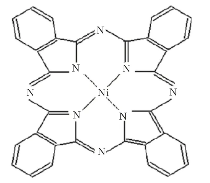
Fig.1. Molecular structure of nickel phthalocyanine.
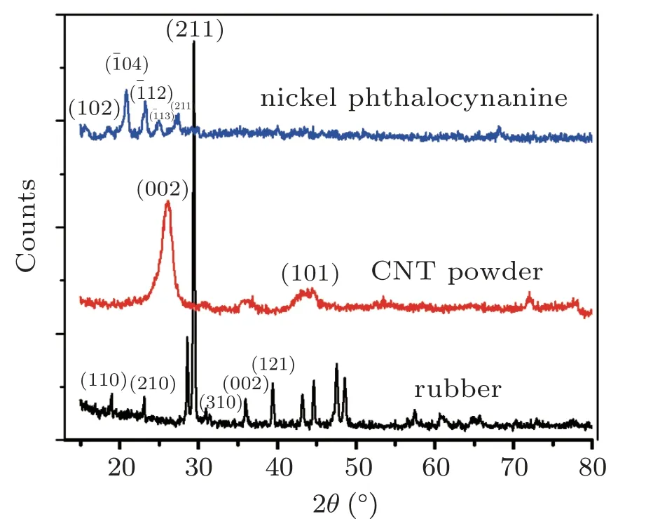
Fig.2. X-ray diffraction patterns of original rubber and CNTs and blue dye(nickel phthalocyanine)powders.
The x-ray diffraction pattern of rubber shows notable high intensity Bragg’s diffraction peaks at 2θ of 18.86◦(110),23.30◦(210), 29.73◦(211), 30.87◦(310), 36.23◦(002), and 39.29◦(121) respectively. These peaks and other peaks present in the rubber x-ray diffractogram are characteristics of polyvinyl chloride which perfectly match with the ICDD data base (PDF# 00-064-1628) and corresponds to high amount of structural arrangement (order) in its polymeric chains.[20]In CNTs powder diffractogram, the broad and major peak of CNTs was observed around 26.22◦(002) which is attributed to the hexagonal graphite structure,having high electrical conductivities. A broad peak of CNTs at 2θ of 44.36◦(101)was also observed. These peaks are consistent with standard xray diffraction data base(PDF#01-075-1621). One additional peak is also observed at 36.23◦because of different functional group attached to the CNTs. The blue dye compound nickel phthalocyanine(C32H16N8Ni)and the peaks are identified using the standard ICDD database (PDF# 00-011-0744) which is also consistent with previous observations.[21]
Deposition of the films by rubbing-in technology described in Refs.[17,18]. The thickness of the NiPc films was in the range of 30 μm–40 μm, while the surface diameter of the NiPc films was found to be about 4.5 mm. The thicknesses of the films were measured using micrometer screw gauge.All samples were fabricated at a pressure of 40 g/cm2. Measurement of the electric properties(I–V characteristics)of the ITO/NiPc/CNT/Rubber cells was carried out under uniaxial pressure of 200,280,and 480 gf/cm2,which were applied perpendicular to the surface of the NiPc film(Fig.3).
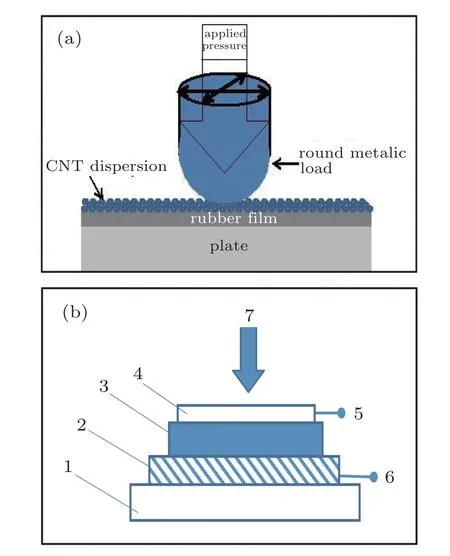
Fig.3. (a)Deposition of the NiPc films on conductive glass(ITO)and carbon nanotube(CNT)films by rubbing-in technology.(b)Schematic diagram of the flexible cell based on ITO/NiPc/CNT/rubber cell. The flexible plastic substrate covered by ITO 1,organic semiconductor NiPc 2,carbon nanotube(CNT)layer 3,rubber 4,and terminals 5 and 6. The arrow 7 shows direction of pressures.
3. Results and discussion
Figure 4 shows the I–V characteristics of the ITO/NiPc/CNT/rubber cell measured at room temperature and at different applied uniaxial pressures of 200, 280, and 480 gf/cm2for the samples from 1 to 3, respectively. One can notice from Fig. 4 that the current response with respect to the applied voltage is a nonlinear curve for all the studied samples. However, the increment in pressure has made the forward potential barrier to be increased compared to the low pressured devices. On the contrary, the higher applied pressure was affected to increase the reverse potential barrier(avalanche region), thereby decreased leaking current due to minority charge carriers. Interestingly, devices with active films prepared under higher pressure can be viably useful for high power electronics application and signal rectification.
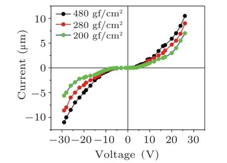
Fig.4. The I–V characteristics of the ITO/NiPc/CNT/rubber cell under various pressures.
It is possible to investigate non-linearity coefficient (α)from the I–V characteristics of the samples using the below expression:[22]
This coefficient can also be determined using the following equation:
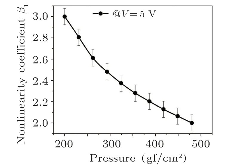
Fig. 5. Non-linearity coefficient β(V) and pressure relationship for ITO/NiPc/CNT/rubber cell.
Figure 5 shows the change in β(V)with the applied pressure for ITO/NiPc/CNT/rubber cells. It is seen that nonlinearity coefficient (β) is in the range of (2–3). Its value is maximum at the pressure of 200 gf/cm2and it is exponentially decreased with increase of the applied pressure up to 480 gf/cm2.The change in the non-linearity of the I–V characteristics might be due to two main effects. First,the decrease in the resistance of the sample and hence increased current through the semiconductor(NiPc). Second,the increased concentration of charge carries, thereby increasing the mobility of charge carriers due to hopping mechanism of conduction which is usually taken place in organic semiconductors.[22]
Also, the phenomenon of non-linearity in the I–V characteristics of organic semiconductors can be observed due to semiconductor–conductor interface defects. Here, the nonlinearity of the studied cells, shown in Fig. 4, can be due to ITO–NiPc and NiPc–CNT contact junctions, which plays the role of two diodes connected opposite to each other.
Figure 6 shows that the rectification ratio in the I–V curve of the ITO/NiPc/CNT/rubber cell is greatly changes with the change of applied pressure. The non-monotonic change in the rectification ratio suggests that the proposed diode structure can be interestingly applied for the application of high-power rectification at selected applied pressures. The presence of a trivial asymmetry in the I–V characteristics can be due to the differences in the work function of ITO and CNT as well as the concentration of the defects present at the concerned interfaces. In particular, the work function of indium tin oxide transparent conductor measured by photoelectron spectroscopy was found to be 4.4 eV to 4.5 eV,[23]while that for the multi-and single-walled carbon nanotubes were estimated to be 4.95 eV and 5.05 eV, respectively.[24]To increase the asymmetry of the I–V characteristics the ITO can be replaced by different conductors having various work functions such as aluminum with work function of 4.06 eV to 4.26 eV.Nevertheless, replacement of ITO by CNT is another approach which has been considered to reduce the cost of materials and to achieve I–V response for desired applications.
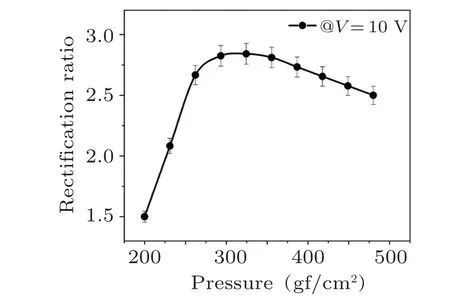
Fig.6. Relationship of the rectification ratio and pressure.
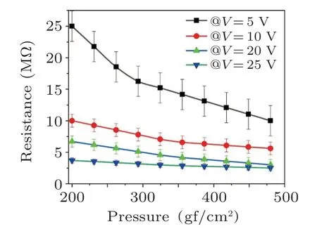
Fig.7. Resistance–pressure relationship at various sweeping voltages.
It is seen that as pressure or applied voltage increased the resistance decreased.The decrease of the resistance can be explained by decrease of the two contact ITO–NiPc and NiPc–CNT resistances as well under effect of pressure,and volume resistance of the NiPc due to decrease of the intermolecular, NiPc–NiPc, distances which accelerate hopping mechanism of the charge carriers transfer. It was observed from the results shown in Figs. 7 and 8 that the resistance of the cells is decreased with the increase of both the applied voltage and pressure. The obtained results show that the flexible ITO/NiPc/CNT/rubber cell fabricated by rubbing-in technology can also be used as pressure sensors due to the changed resistance of the device with the pressure.
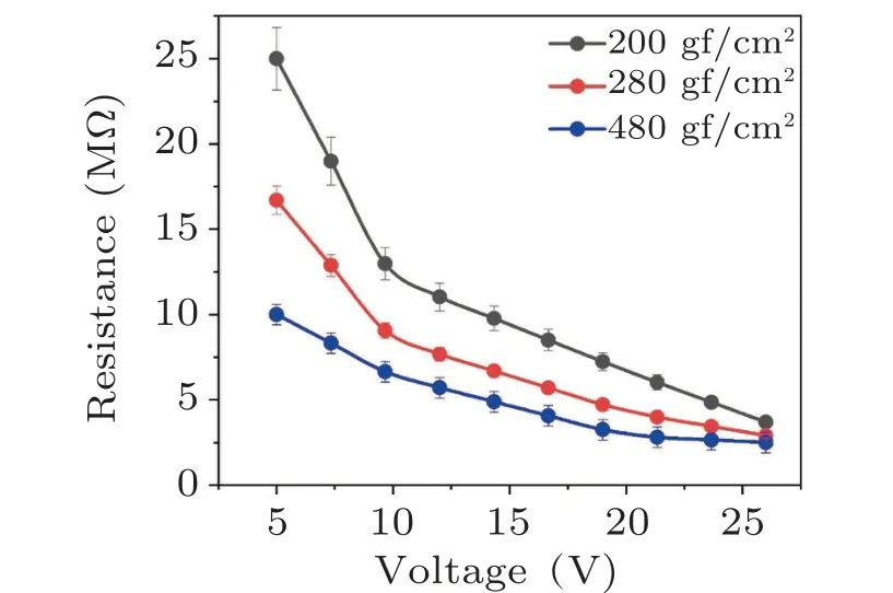
Fig. 8. Dependences of the resistance of the ITO–NiPc–CNT samples on applied voltage at different pressures.
4. Conclusion
The nickel phthalocyanine (NiPc) film was successfully fabricated by rubbing-in technology on the surface of flexible ITO glass substrate and the I–V characteristics of the ITO/NiPc/CNT/rubber devices were investigated under uniaxial pressures of 200, 280, and 480 gf/cm2. It was concluded that the cell resistance is decreased with the increase of pressure and voltage. The nonlinearity coefficient of the I–V characteristics of the samples was found to be about 2 to 3,which was decreased with the increase of the pressure. The rectification ratio of the cells was estimated to be dependent on the applied pressure. The results presented here can be potentially used for the fabrication of rubbing-in technology based electronic devices such as diodes,non-linear resistors and sensors.
杂志排行

Chinese Physics B的其它文章
- Two-dimensional finite element mesh generation algorithm for electromagnetic field calculation*
- Stable water droplets on composite structures formed by embedded water into fully hydroxylated β-cristobalite silica*
- Surface active agents stabilize nanodroplets and enhance haze formation*
- Synchronization mechanism of clapping rhythms in mutual interacting individuals*
- Theoretical study of the hyperfine interaction constants,Land´e g-factors,and electric quadrupole moments for the low-lying states of the 61Niq+(q=11,12,14,and 15)ions*
- Ultrafast photoionization of ions and molecules by orthogonally polarized intense laser pulses: Effects of the time delay*