Strain-induced the dark current characteristics in InAs/GaSb type-II superlattice for mid-wave detector
2020-06-18LeeKoKimandNah
H. J. Lee , S. Y. Ko Y. H. Kim and J. Nah,
1i3system, Inc., 26-32, Gajeongbuk-ro, Daejeon, 34113, Yuseong-gu, Korea
2Department of Electrical Engineering, Chungnam National University, Daejeon, 34134, Yuseong-gu, Korea
Abstract: Type-II superlattice (T2SL) materials are the key element for infrared (IR) detectors. However, it is well known that the characteristics of the detectors with the T2SL layer are greatly affected by the strain developed during the growth process,which determines the performance of IR detectors. Therefore, great efforts have been made to properly control the strain effect and develop relevant analysis methods to evaluate the strain-induced dark current characteristics. In this work, we report the strain-induced dark current characteristics in InAs/GaSb T2SL MWIR photodetector. The overall strain of InAs/GaSb T2SL layer was analyzed by both high-resolution X-ray diffraction (HRXRD) and the dark current measured from the absorber layer at the elevated temperatures (≥ 110 K), where the major leakage current component is originated from the reduced minority carrier lifetime in the absorber layer. Our findings indicate that minority carrier lifetime increases as the tensile strain on the InAs/GaSb T2SL is more compensated by the compressive strain through ‘InSb-like’ interface, which reduces the dark current density of the device. Specifically, tensile strain compensated devices exhibited the dark current density of less than 2 ×10⁻⁵ A/cm2 at 120 K, which is more than one order of magnitude lower value compared to that of the device without tensile strain relaxation.
Key words: mid-wave detector; InAs/GaSb type II super lattice; dark current
1. Introduction
There is an increasing demand for infrared detectors in a wide variety of applications, such as surveillance equipment,medical devices, and military applications. To date, InSb and HgCdTe (MCT) have been the main block for conventional infrared detectors because they demonstrate relatively high quantum efficiency and low dark current[1]. Recently, type-II superlattice (T2SL) has gained increasing attention and has replaced InSb or MCT infrared detectors[2,3].
One of the crucial factors determining the performance of T2SL detector is the growth quality of the epitaxial (epi.) layer, which is closely related to balanced strain[4]by the small lattice mismatch between InAs and GaSb[5]. If the strain of T2SL is not properly balanced, then it can lead to the formation of extended defects that act as Shockley-Read-Hall (SRH) recombination lefts. In InAs/GaSb T2SL, anions and cations are often exchanged across the interface that has no-commonatom. This “non-common-atom” can introduce new interfacial bonds exhibiting 'InSb-like' or 'GaAs-like' characteristics at the interface between InAs and GaSb[6]. This intermixing between the binary layers (InAs and GaSb) can unintentionally occur even if fast shutter switching is possible with the advancement of molecular beam epitaxy (MBE) growth technology (e.g., As in GaSb or Sb in InAs), which has a strong impact on the structural, electrical and optical properties of InAs/GaSb T2SL[7]. In the case of 'InSb-like' interface, due to larger lattice constant of InSb compared with that of GaSb substrate, the few monolayers (MLs) of 'InSb-like' interface between InAs and GaSb can compressively strain the T2SL[8].Therefore, several efforts have been made to introduce an'InSb-like' layer at the interface between InAs and GaSb in order to compensate the tensile strain[9−17]. This 'InSb-like' interfacial layer has been confirmed by analyzing the structural properties of InAs/GaSb T2SL layer by high-resolution X-ray diffraction (HRXRD), high-angle annular dark-field (HAADF), transmission electron microscope (TEM) and atom probe tomography (APT)[14−17]. Zhanget al. in 2011 and Songet al. in 2013 reported the optical properties of InAs/GaSb T2SL layer with an 'InSb-like' interfacial layer using photoluminescence(PL)[12,13]. Zuoet al. in 2013 reported that the 'InSb-like' interfacial layer is closely related with the dark current characteristics of InAs/GaSb T2SL layer by investigating the minority carrier lifetime using electron beam induced current (EBIC)[11].Thus, electrical and structural analysis method should be correlated to determine the 'InSb-like' interfacial layer as it plays a very important role in improving the performance of InAs/GaSb T2SL detectors.
In this work, we report that the interfacial properties of InAs/GaSb T2SL layer can be largely varied even if the epi.wafers are prepared by the same MBE protocol, significantly affecting the dark current characteristics of the devices. By analyzing temperature-dependent dark current characteristics and spectral responses of the T2SL layer, the properties of the interfacial layer have been investigated. Further, the strain of InAs/GaSb T2SL layer was also verified by analyzing the mismatch using the HRXRD patterns. Our study indicates that the minority carrier lifetime significantly increased as the tensile strain on the InAs/GaSb T2SL is more compensated by compressive strain originated from the 'InSb-like' interface, reducing the dark current density of the devices. Consequently,the dark current density of the fabricated devices on the strain compensated InAs/GaSb T2SL layer demonstrates the dark current density less than 2 × 10⁻⁵A/cm2at 120 K.

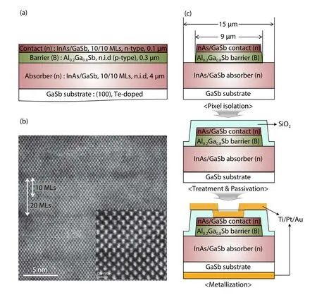
Fig. 1. (Color online) (a) The schematic of the InAs/GaSb T2SL MWIR epi. structure with nBn structure. (b) TEM image of the absorber layer with InAs/GaSb 10/10 MLs. The inset on right corner shows a magnitude view taken in HAADF mode. (c) The schematics of the InAs/GaSb T2SL nBn device fabrication process. Fist, each pixel is isolated by etching the top contact layer and the barrier using C6H8O7/H3PO4/H2O2/H2O solution.After wet-treatment to remove a native oxide at the surface, SiO2 passivation layer is deposited using PECVD. Finally, the contact metal is evaporated for both pixels and common electrode.
2. Experiments
The crystal structure of the InAs/GaSb T2SL mid-wave infrared (MWIR) studied in this work is shown in Fig. 1(a). The absorber layer consists of InAs/GaSb 10/10 MLs, which has a bandgap energy of 0.244 eV, calculated using empirical pseudopotential method (EPM) at 77 K. The absorber layer in Fig. 1(b) clearly shows the periodic crystal structure, where the inset shows dumbbell-like structures of InAs and GaSb.To compose nBn structure that can effectively reduce the dark current, the barrier layer was designed with Al0.2Ga0.8Sb that has a relatively high conduction band energy barrier(~ 1 eV) with almost zero valence band offset. For experiment, two different wafers (A and B) were grown individually but with the identical design and the same MBE protocol. Using two different epi. wafers, InAs/GaSb T2SL nBn devices with a 15μm pitch were fabricated as briefly described in Fig. 1(c). Here, each pixel is isolated in 9 × 9 cm2area by etching the top contact layer and the barrier layer using C6H8O7:H3PO4: H2O2: H2O (15 : 20 : 12 : 40) solution for 25 s, followed by immersing in HCl : H2O (1 : 10) solution for 60 s to remove a native oxide at the surface. For passivation, a 300 nm-thick SiO2was deposited using a plasma-enhanced chemical vapor deposition (PECVD) at 250 °C for 45 s. Afterwards, Ti/Pt/Au (30/70/100 nm) layer was deposited on the contact layer of each pixel on the top side and on the GaSb substrate as a bottom common electrode for the electrical characterization.
3. Results and discussion
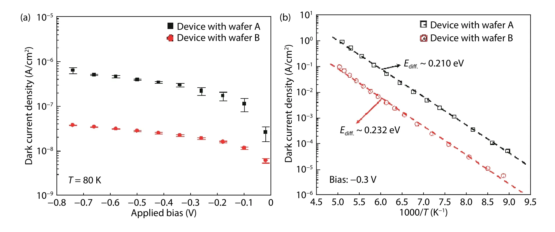
Fig. 2(a) shows the dark current density of the devices fabricated on the wafers A and B which are measured at 80 K.We note that the identical fabrication process is employed for the devices on both wafers A and B. The devices on two different wafers exhibit approximately one order of magnitude difference in the dark current density even if the same device design and process are employed. The dark current at cryogenic temperature (80 K) could be originated from different parts of the device. For example, it can be either from the depletion region in the vicinity between the barrier and the absorber or from the surface region covered with the passivation film. Thus, to further investigate the devices, the dark current density was measured by increasing temperature to 200 K. As the temperature increases, the dark current density is dominated by the diffusion current and recombination current from the absorber layer, which is greatly affected by the crystal quality of absorber layer rather than the process condition.

Fig. 2. (Color online) (a) The dark current density versus applied bias at 80 K. The identical fabrication process is used for device fabrication on the wafers A and B. Approximately, one order of magnitude higher dark current density is observed from the devices on the wafer A. (b) Arrhenius plots of the devices fabricated on the wafers A and B. Both devices demonstrate diffusion-limited current but different activation energies. The plot indicates that the minority carrier lifetime in the absorber layer of the devices on the wafer B is longer than those on the wafer A.

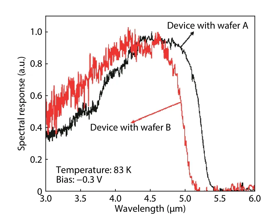
Fig. 3. (Color online) Spectral response of the devices fabricated on the wafers A and B. The cut-off wavelength of the devices on the wafer B is shorter than those on the wafer A. The result is consistent with the results in Fig. 2, exhibiting difference activation energies.
Next, temperature-dependent dark current density was measured at a bias voltage of -0.3 V for the devices on two different wafers as shown in Fig. 2(b). Both devices demonstrate the diffusion-limited dark current characteristics but with slightly different activation energies. The dark current density of the devices fabricated on the wafer B is approximately one order smaller than those on the wafer A. This result shows that the minority carrier lifetime in the absorber layer of the wafer B is longer than that of wafer A. Different minority carrier lifetime can be attributed to overall strain on the InAs/GaSb T2SL layer. Unbalanced strain can lead to the formation of extended defects that act as SRH recombination lefts[4], reducing the minority carrier lifetime[11]. Especially, the dark current density of the fabricated devices on the wafer B are less than 2 × 10⁻⁵A/cm2at 120 K, which is similar to or excels the value recently reported using the same T2SL structure[18, 19].

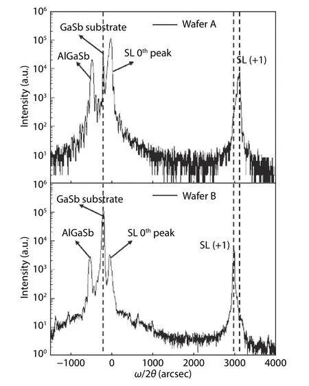
Fig. 4. High-resolution X-ray omega-2theta scan data of InAs/GaSb T2SL and Al0.2Ga0.8Sb around GaSb (004) peak.
The overall strain on the T2SL affects not only the electrical properties as described above but also the optical properties[5,8,11−13]. Fig. 3 shows the spectral responses of the devices fabricated on the wafers A and B, which were characterized using Fourier transform infrared (FTIR) spectrometer.The devices exhibit 40 % cut-off wavelength of 5.25μm for the wafer A and 5μm for the wafer B at 83 K. This result indicates that the activation energy of the devices fabricated on wafer B is larger than that of the devices on wafer A, confirming different absorber layer properties of two wafers and is also consistent with the results in Fig. 2(b). The energy bandgap of the absorber layers of the T2SL can be significantly varied despite of the identical design, MBE protocol,and the device fabrication process. Therefore, the growth quality of the T2SL layer can strongly affect the performance of the devices.
To further unveil the origin of different electrical and optical properties, HRXRD pattern was measured to compare the overall strain of the wafers A and B. Fig. 4 qualitatively showsthe difference in the peak between GaSb substrate and the first superlattice (SL). The SL (+1) peak of the wafer B is closer to GaSb substrate than that of the wafer A. As shown in Table 1. the average lattice mismatch and periodicity obtained from HRXRD pattern quantitatively show different T2SL quality of the wafers A and B. The thickness of one period InAs/GaSb T2SL (periodicity) is calculated to be 59.18 Å for wafer A and 59.06 Å for wafer B, respectively. Although the periodicity of both wafers A and B is close to the original layer design and the growth of InAs/GaSb T2SL layer has been performed as expected; however, the mismatch values are clearly different: the mismatch of wafers A and B are 788.6 and 67.37 ppm, respectively. We believed that randomly formed 'InSb-like' interfacial layer during the MBE process greatly reduced the mismatch. The results of the HRXRD pattern in Table 1 and the dark current characteristics in Fig. 2 clearly demonstrate that overall strain on InAs/GaSb T2SL layer affects the minority carrier lifetime[7,10,11,13], where the minority carrier lifetime could be increased by one order of magnitude due to the balanced strain.

Table 1. Analysis of HRXRD patterns.
4. Conclusion
In this work, the electrical, optical and structural properties of the InAs/GaSb T2SL MWIR epi. structures were analyzed. Using dark current density measurement, FTIR and HRXRD analysis, the interfacial property of the InAs/GaSb T2SL layer has been successfully analyzed. The results demonstrate that the minority carrier lifetime can be extended by compensating the tensile strain of the InAs/GaSb T2SL layer through unintentionally formed 'InSb-like' interfacial layer during the MBE growth process. Through strain compensation of the tensile strained InAs/GaSb T2SL layer, the dark current density smaller than 2 × 10⁻⁵A/cm2has been achieved at 120 K. Therefore, high performance InAs/GaSb T2SL MWIR photodetectors can be fabricated reproducibly by developing the growth process to intentionally form 'InSb-like' interfacial layer.
Acknowledgements
This research was supported by the research fund of Chungnam National University and the author would like to A. Liu at IQE for helpful discussions. The authors wish also to thank his colleagues at i3system, Inc. for processing of the devices.
杂志排行
Journal of Semiconductors的其它文章
- A brief review of formation energies calculation of surfaces and edges in semiconductors
- Coupling between quantum dots and photonic nanostructures
- A review on performance comparison of advanced MOSFET structures below 45 nm technology node
- Modelling and optical response of a compressive-strained AlGaN/GaN quantum well laser diode
- A 0.1-1.5 GHz multi-octave quadruple-stacked CMOS power amplifier
- A high performance adaptive on-time controlled valley-currentmode DC-DC buck converter
