Simulation analysis of a high efficiency GaInP/Si multijunction solar cell
2020-03-16BenaichaDehimiPezzimentiandBouzid4LaboratoryofMetallicandSemiconductorMaterialsUniversityofBiskraBiskra07000Algeria
M. Benaicha, L. Dehimi, , F. Pezzimenti , and F. Bouzid4Laboratory of Metallic and Semiconductor Materials, University of Biskra, Biskra 07000, Algeria
2Faculty of Science, University of Batna, Batna 05000, Algeria
3DIIES - Mediterranea University of Reggio Calabria, Reggio Calabria 89122, Italy
4UDCMA - Research Center in Industrial Technologies, Algiers 16014, Algeria
Abstract: The solar power conversion efficiency of a gallium indium phosphide (GaInP)/silicon (Si) tandem solar cell has been investigated by means of a physical device simulator considering both mechanically stacked and monolithic structures. In particular, to interconnect the bottom and top sub-cells of the monolithic tandem, a gallium arsenide (GaAs)-based tunnel-junction,i.e. GaAs(n+)/GaAs(p+), which assures a low electrical resistance and an optically low-loss connection, has been considered. The J–V characteristics of the single junction cells, monolithic tandem, and mechanically stacked structure have been calculated extracting the main photovoltaic parameters. An analysis of the tunnel-junction behaviour has been also developed. The mechanically stacked cell achieves an efficiency of 24.27% whereas the monolithic tandem reaches an efficiency of 31.11% under AM1.5 spectral conditions. External quantum efficiency simulations have evaluated the useful wavelength range. The results and discussion could be helpful in designing high efficiency monolithic multijunction GaInP/Si solar cells involving a thin GaAs(n+)/GaAs(p+) tunnel junction.
Key words: GaInP/Si; tandem solar cells; power efficiency; numerical simulations
1. Introduction
Solar photovoltaics (PV) is a continuously growing technology ascertained as one of the most promising candidates to reduce the fossil fuel energy demand for the next decades in a large number of space and terrestrial applications.
Nowadays the research on PV is focused on deploying new materials and/or complex device structures[1-9]. In this context, multijunction solar cells based on III–V semiconductors aid to compensate the spectral sensitivity by increasing the spectral absorption range[10,11]. High efficiencies on the order of 43.5% have been already demonstrated for GaInP/GaAs/GaInNAs solar cells[12]. However, the optimizing solar cell performance with cost reduction remains a key issue for designers and the monolithic integration on silicon(Si) substrates is a practical way to reduce the manufacturing costs of tandem cells by reducing the cost of the starting material[13-17].
In more detail, III–V/Si multijunction solar cells have achieved efficiencies around 30% for monolithic InGaN/Si two-junction structures[18], and 35% for In0.46Ga0.54N/Si tandem solar cells[19]. In addition, simulation studies have showed that efficiencies in excess of 33% can be calculated for AlxGa1–xAs/epi-Si(Ge) solar cells[20]. At the same time, a mechanically stacked GaInP/Si tandem reaching an efficiency of 27% under 1 sun has been demonstrated in Ref. [21] by using an optimized structure that involves anti-reflection coating and passivation layers at the frontside of the top and bottom cell, respectively.
In this paper, both mechanically stacked and monolithic multijunction (MMJ) GaInP/Si solar cells are investigated. In particular, the sub-cells of the monolithic device are interconnected by considering a GaAs(n+)/GaAs(p+) tunnel-junction which allows, in principle, a current flow through the structure minimizing the voltage drops[22]. In fact, depending on the Ga composition, the In1–xGaxP alloy can be grown on a GaAs substrate with an appropriate lattice match as investigated experimentally in Ref. [23]. The choice of a GaAs(n+)/GaAs(p+) tunnel-junction in designing a III–V/Si multijunction solar cell is also supported by an our previous study presented in Ref. [19].
The fundamental PV parameters, such as the open circuit voltage (Voc), short circuit current density (Jsc), fill factor(FF), and conversion efficiency (η) have been calculated under AM1.5 spectral conditions. In particular, the mechanically stacked tandem and the monolithic tandem achieve an efficiency of 24.27% and 31.11%, respectively.
2. Device structure and modelling
The schematic cross-section of the proposed MMJ GaInP/Si solar cell is shown in Fig. 1. The drawing is not to scale.
We consider a GaInP top-cell, with a material bandgap energy of 1.8 eV, and a conventional Si bottom-cell connected in series by means of a GaAs(n+)/GaAs(p+) tunnel-junction. Detailed information for the different layers is given in Table 1.

Fig. 1. (Color online) Schematic cross-section of the MMJ GaInP/Si solar cell.

Table 1. Structure of the simulated GaInP/Si MMJ tandem cell.
In the top-cell, the back-surface field (BSF) layer and the window layer are assumed to reduce the surface recombination velocity and the scattering of carriers towards the tunnel-junction (TJ), respectively. These two layers have the same thickness (20 nm) and net doping (2 × 1018cm–3). The TJ is a highly doped (5 × 1019cm–3) ultra-thin layer with a thickness of 50 nm. This TJ structure has been already investigated in Ref. [19] appearing, with an overall thickness in the limit of 60 nm, well suited for the design of high efficiency III–V/Si multijunction solar cells.
The modelling activity has been performed by using the Silvaco-TCAD numerical simulation software to solve Poisson’s equation and continuity equations for carriers under steady state conditions. The solar cell has been investigated under AM1.5 radiation (100 mW/cm2) and photons are assumed to be incident from the p-GaInP side of the GaInP topcell. Recent papers addressing the modelling of different devices support the considered simulation setup as briefly recalled in the following[24-27]. In particular, it involves the effective density of states, and the doping-dependent recombination processes and carrier mobilities. Also, specific expressions depending on In composition in the GaInP regions,such as the bandgap energy, electron affinity, and relative permittivity, are taken into account.
The fundamental InxGa1–xP material parameters are calculated using the physical models summarized in Table 2.
Two of the most critical parameters for advanced solar cell modelling are the material refractive index, n, and the extinction coefficient, K. Because of the difficulty in collecting optical parameters for many ternary and quaternary materials, a good approximation of n and K may be obtained by interpolating simpler compounds data. In particular, the interpolation between the GaP and InP data allows to estimate the op-tical parameters for the Ga0.5In0.5P compound as shown in Fig. 2[33].

Table 2. Physical models.
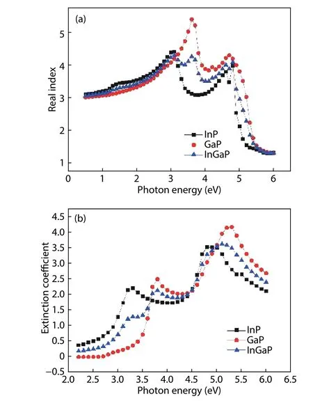
Fig. 2. (Color online) Interpolation of (a) n and (b) K for Ga0.5In0.5P.
Finally, the absorption coefficient for the Si substrate is calculated by the following expressions[34]:

for 1.12 ≤ E < 1.5 eV and E ≥ 1.5 eV, respectively.
3. Tunnel-junction behaviour
In multijunction solar cells, the TJ shorts the n/p regions of the adjacent sub-cells and the tandem structure can be de facto treated as a single junction cell[35]. Nowadays, the TJ plays a key role once the photocurrent losses from light absorption in this region are minimized. In other words, the TJ design should be transparent to the wavelengths absorbed by the series-connected sub-cells and also forming a low-resistive interface which assures minimal voltage drops.

Fig. 3. (Color online) J–V curve of the GaAs(n+)/GaAs(p+) TJ in dark.
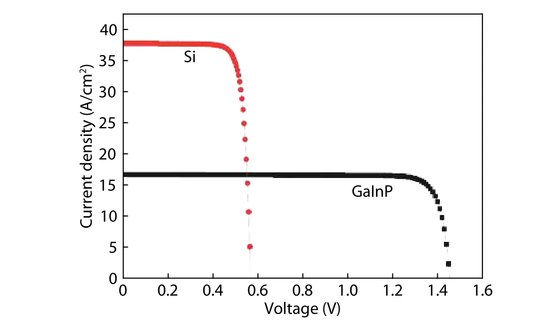
Fig. 4. (Color online) J–V characteristics of the Si and GaInP single cells.
Basically, the TJ is a degenerately doped p/n junction which leads to quantum tunneling phenomena for electrons in forward-bias. The relative expression of the current density is the form of Ref. [22],

where EFRand EFLare the Fermi levels in the valence and conduction band, respectively, and T(E) is the tunneling probability expressed by the Wentzel–Kramers–Brillouin theory assuming the electron wave function k(x) as an exponential term integrated over the depletion region as follows:Here, x1and x2are the edges of the depletion region.

As introduced in the previous section, in this study we have considered a highly doped GaAs(n+)/GaAs(p+) TJ between the GaInP and Si regions of the GaInP/Si MMJ solar cell. This improves the cell efficiency as discussed in Refs. [29, 35]. The simulated J–V curve of the TJ in dark is shown in Fig. 3.
The design structure has a peak of the tunneling current density close to 22 A/cm2. This value has to be higher than the Jscvalue of the relative solar cell to satisfy the so called“first criteria” for the MMJ design[36]. Moreover, a resistance as low as 4 mΩ·cm2can be calculated from Fig. 3 at the aforementioned current density.
4. Results and discussion
4.1. GaInP and Si single cells
The proposed multijunction cell is structured with two stacked GaInP and Si cells. These two cells are firstly investigated individually. This way, their electrical characteristics have been properly adjusted and the resulting J–V curves are shown in Fig. 4.
The PV parameters extracted for each cell, namely the open circuit voltage, Voc, the short circuit current density, Jsc,the fill factor, FF, and the conversion efficiency, η, are listed in Table 3. As we can see, due to the material wide bandgap,the GaInP single cell generates a large Vocof 1.45 V and a Jscof 16.75 mA/cm2. These values are in good agreement with those measured in Ref. [37] where a comparable GaInP single junction solar cell with η = 20.8% has been characterized.Also, they validate the adopted simulation setup in providing reliable results with an error in the conversion efficiency calculation associated to the uncertainty of some simulation parameters which is in the limit of 0.5%. This range of variability is consistent with the results reported in Ref. [21].

Table 3. PV parameters extracted from Fig. 4.
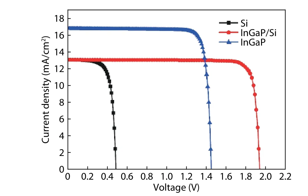
Fig. 5. (Color online) J–V curve for both the single junction cells and the InGaP tandem structure.
4.2. Mechanically stacked structure
In this section, we present the simulation results obtained when the GaInP and Si solar cells are next placed in a mechanically stacked configuration by means of a transparent adhesive layer. The J–V behaviour for both the single junction cells and the tandem structure are shown in Fig. 5.
As expected, the J–V curve of the top-cell is unaffected and it appears as in Fig. 4. Contrariwise, the bottom-cell produces less current due to fact that higher energy photons are absorbed by the top-cell. From Fig. 5, the extracted PV parameters are listed in Table 4.
To obtain detailed information about the useful wavelength range in the tandem structure, external quantum efficiency (EQE) simulations have been performed. The EQE of the GaInP top-cell and Si bottom-cell under 1-sun AM1.5 illumination is shown in Fig. 6.
As we can see, the top-cell has a greater collection efficiency for carriers generated by shorter wavelengths while the bottom-cell has a greater collection efficiency for carriersgenerated by longer wavelengths. Therefore, these two cells can be considered complementary in a tandem structure although an optimized design in terms of geometrical and physical parameters should be also addressed to the shrinkage of the EQE transition region as much as possible. For example,in Fig. 6, the EQE is limited to about 0.2 in the wavelength range from 0.65 to 0.7 μm.

Table 4. PV parameters extracted from Fig. 5.

Fig. 6. (Color online) EQE of the GaInP top-cell and Si bottom-cell in the stacked structure.
4.3. Multi-junction solar cell
By placing the GaAs(n+)/GaAs(p+) TJ in the vertical stacking of the GaInP and Si single cells, we can investigate the MMJ structure. The corresponding band diagram of the GaInP/Si tandem cell at thermodynamic equilibrium is shown in Fig. 7(a). In this bias condition, the electron quasi Fermi level (QFL) is a constant across the structure.
We can note that the TJ is located around 1.15 μm from the top surface and in fact, at this depth, the electric field profile along the cell exhibits a peak value as high as 3.5 MV/cm as shown in Fig. 7(b).
Here, the energy levels behaviours originate a tunnel region that leads to carrier recombination phenomena. In other words, the band energy levels bend sufficiently to allow carriers to tunnel by internal field emission.
Finally, the simulated J–V curve of the MMJ solar cell is shown in Fig. 8. Here, the current behaviour of the mechanical stacked structure in Fig. 5 is also reported for comparison.The extracted PV parameters are summarized in Table 5.
We obtain a conversion efficiency of 31.11% for the MMJ structure involving an optimized tunnel junction, which is higher than 24.27% calculated for the mechanically stacked cell.
It is worthwhile noting that, by comparing the simulation results of the mechanically stacked cell with respect to the measurements reported in Ref. [21] for a mechanically stacked 4-terminal GaInP/Si tandem cell performing a conversion efficiency close to 27%, the resulting efficiency difference (about 2 percentage-points) is mainly due to the performance of the conventional Si-based bottom cell. In fact, since the optimized design of the Si single cell was not investigated in this work, before stacking it achieves 17.45% as reported in Table 3 against 19.7% in Ref. [21] where anti-reflection coating and passivation layers are added at the frontside for optimization.
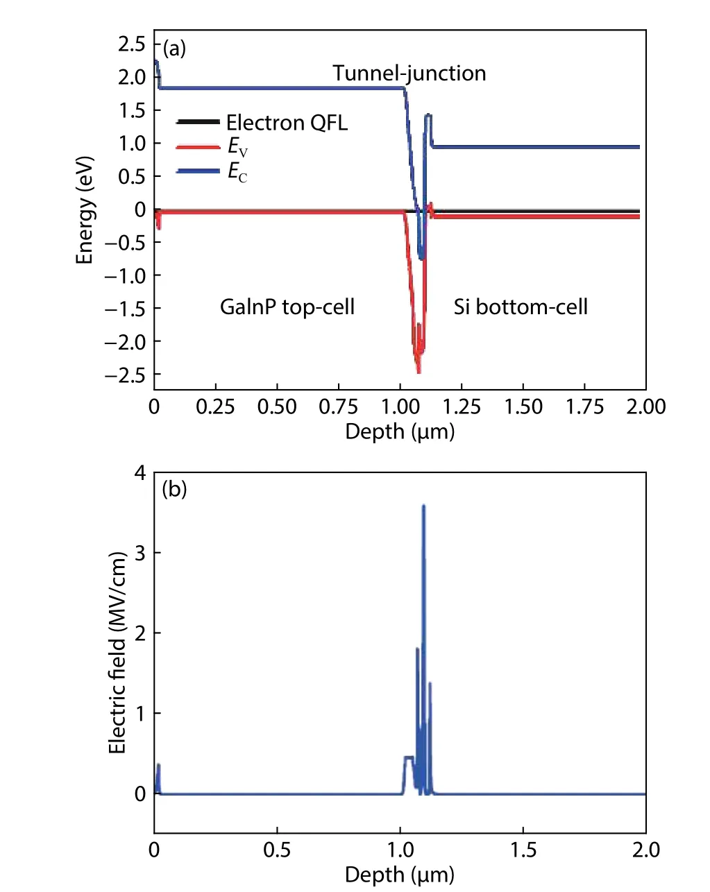
Fig. 7. (Color online) (a) Energy band diagram of the GaInP/Si tandem cell at thermodynamic equilibrium; EV and EC are the energy levels of the valence and conduction band, respectively. (b) Electric field profile.

Fig. 8. (Color online) Comparison between the J–V curves of the MMJ tandem cell and the GaInP/Si mechanical stacked structure.

Table 5. PV parameters of the proposed GaInP/Si tandem solar cells.
5. Conclusion
In this paper GaInP/Si tandem solar cells have been analysed by using a physical device simulator. During the simulations, we considered both mechanically stacked and monolithic multi-junction structures that involve a relative thin GaAs(n+)/GaAs(p+) tunnel junction. By extracting the main photovoltaic parameters from the J–V curves, the first design shows an efficiency of 24.27% whereas the latter achieves an efficiency of 31.11% under AM1.5 spectral conditions. The obtained results have been compared with literature data to validate the adopted simulation setup in providing reliable results that avoid an overestimation of the model in the calculation of the PV parameters. The developed analysis could be the theoretical basis for the design of high efficiency MMJ GaInP/Si solar cells with an optimized GaAs(n+)/GaAs(p+) tunnel junction.
杂志排行
Journal of Semiconductors的其它文章
- Epitaxial graphene gas sensors on SiC substrate with high sensitivity
- Observation of exciton polariton condensation in a perovskite lattice at room temperature
- Small-signal modeling and parameter extraction method for a multigate GaAs pHEMT switch
- Influence of self-heating on the millimeter-wave and terahertz performance of MBE grown silicon IMPATT diodes
- First-principles exploration of defect-pairs in GaN
- High performance GaN-based hybrid white micro-LEDs integrated with quantum-dots
