A routing algorithm for FPGAs with time-multiplexed interconnects
2020-02-28RuiqiLuoXiaoleiChenandYajunHa
Ruiqi Luo , Xiaolei Chen, and Yajun Ha
1School of Information Science and Technology, ShanghaiTech University, Shanghai 201210, China
2Shanghai Institute of Microsystem and Information Technology, Chinese Academy of Sciences, Shanghai 200050, China
3University of Chinese Academy of Sciences, Beijing 100049, China
4Intel Singapore, Singapore 339510, Singapore
Abstract: Previous studies show that interconnects occupy a large portion of the timing budget and area in FPGAs. In this work, we propose a time-multiplexing technique on FPGA interconnects. In order to fully exploit this interconnect architecture,we propose a time-multiplexed routing algorithm that can actively identify qualified nets and schedule them to multiplexable wires. We validate the algorithm by using the router to implement 20 benchmark circuits to time-multiplexed FPGAs. We achieve a 38% smaller minimum channel width and 3.8% smaller circuit critical path delay compared with the state-of-the-art architecture router when a wire can be time-multiplexed six times in a cycle.
Key words: field programmable gate arrays; digital integrated circuits; routing algorithm design and analysis; digital integrated circuits
1. Introduction
Interconnect and logic resources can be seen as the two significant parts of FPGAs. Logic blocks are used to implement a user design. Interconnect resources are designed to achieve connections among logic blocks. In FPGAs, logic resources are always organized as arrays of blocks. Interconnect resources are routing switches and wires grouped into channels. FPGA interconnects (or interconnection network)can be thought of as a programmable network of signal paths among FPGA logic resource ports.
Both measurements and analyses indicate that the programmable interconnections contribute the most to the FPGA area, latency, and power consumption. In order to achieve high routability with reduced routing, FPGA vendors use the substantial on-chip area to route programmable switches and wires[1]. This is why interconnects out-weight logic in terms of power budget and area. FPGA interconnects are slow because they need to traverse a series of tracks connected by switches to route among different logic blocks. Optimizing the interconnect network is critical because it has a profound impact on the performance of FPGAs.
Previous work by Trimberger et al.[2]has illustrated that the utilization of logic resources in FPGA can be improved by time-multiplexing, which inspires us to apply time-multiplexing to FPGA interconnection networks and leads to our new architecture and routing algorithm that we will introduce in this paper. We notice that most wires are only used for a short period in a clock cycle. The delay of wire for a signal is only a small portion in a clock cycle. So we can better utilize the interconnect resources by time-multiplexing signals. It can also improve the FPGA performance at a small cost of the multiplexing circuitry complexity.
FPGAs with time-multiplexed interconnects require specialized electric design automation (EDA) algorithms and tools to support them. Existing algorithms and tools cannot be reused in their present forms because they are not multiplexing-aware. In this paper, we propose a time-multiplexingaware routing algorithm. This algorithm is similar to VPR routing algorithm[3]. Unlike the VPR algorithm, our algorithm can add the time-multiplex feature to the algorithm and implement it. In order to achieve this feature, we also design TM switches which are described in an architecture file. We define a bitmap for signals in our design, which is a new technique and can add the scheduling capability to the VPR algorithm. This algorithm can be seen as timing-driven because it has a delay-sensitive term in its multiplexing-aware congestion cost function.
We also validate our proposed routing algorithm experimentally. We evaluate our TM-ARCH FPGAs by using our TMrouter to replace the conventional VPR router in a standard FPGA EDA flow. We also use the VPR 5 router[4]as a comparison on the same set of benchmark circuits with conventional architecture. Experimental results reveal that we only use 65% average minimum channel width of conventional architectures on average and can achieve 3.8% smaller circuit critical path delay on average.
The rest of this paper is as follows. Section 2 introduces existing FPGA architectures and their EDA algorithms. Section 3 briefly introduces TM-ARCH architecture. Section 4 proposes our time-multiplexing-aware routing algorithm. Section 5 introduces what we have done to validate this algorithm, and also presents experimental results. Finally, Section 6 concludes this paper.
2. Related work
Previous work on time-multiplexed FPGA[2]has been done. Trimberger et al. propose both time-multiplexed interconnects and configurable logic blocks (CLBs) with the Xilinx XC4000E FPGA family. To facilitate mapping user designs into time-multiplexed architecture, a scheduling algorithm is presented[5]that is based on list scheduling. Lin et al. also apply time-multiplexing to Xilinx 4000 architecture FPGA[6], but they only time-multiplex routing resources. Even so, they still have achieved 30% reduction of channel density. Francis et al.[7]apply time-multiplexed interconnects to an Altera FPGA, which is similar to our architecture proposed in this paper. Only interconnects are time-multiplexed in ours, Lin's and Francis’ work, while both logic blocks and interconnects are time-multiplexed in Trimberger’s architecture. In terms of the supporting EDA flow, Trimberger’s work can be considered as close to ours in both works, time-multiplexing is scheduled after technology mapping and before placement. In our work, time-multiplexing is scheduled during routing, while Francis’ work does it after routing.
Shen et al. present a serial-equivalent static and dynamic parallel router[8]. This router provides a significant speedup in routing and can achieve the same result as the serial router. They also try box expansion and grid partitioning to speed up parallel FPGA routing[9]. Shen et al. use parallel recursive partitioning to accelerate FPGA routing that can achieve 7.06× speed up using 32 processers[10]. They propose a GPU-based parallel routing algorithm[11]and achieved 1.57× speedup improvement than VPR router. Based on PathFinder kernel, they develop Raparo, which is an angle based region partitioning[12]. Results show that it can provide 16× speedup when scaling to 32 processor cores. They also exploit strictly-ordered partitioning in parallelizing FPGA routing called Megrez and achieve 15.13× speed up on GPU without influence on quality[13].
Vercruyce et al. propose CRoute[14], which is a connection-based timing-driven router. This routing algorithm can reduce total wire-length and increase the maximum clock frequency at the same time. Wang et al. propose a new approach[15]based on the PathFinder algorithm. They only reroute illegal paths during each routing iteration and can reduce 68.5% routing runtime on average. Patil et al. use a heuristic method in routing for hybrid FPGA networks[16]. They schedule data streams efficiently to increase the bandwidth and then achieve 11% stream bandwidth improvement on five benchmark circuits. Chaplygin et al. propose an FPGA routing block optimization with a given number of trace signals[17]. Farooq et al. apply the time-multiplexing technology to multi-FPGA prototyping routing for more complicated designs[18]. Omam et al. use RRAM-based switches and decrease 56% path delay compared to CMOS base switches[19].Chen et al. explore state-of-the-art research directions for FPGA placement and routing[20]. Huriaux et al. evaluate the routing of I/O signals of large applications through column interfaces in embedded FPGA fabrics[21]. Kashif et al. compare a completely connected graph and time-multiplexing nets on multi-FPGA system[22]. Results show that completely connected graphs can achieve higher performance and time-multiplexing can provide a better cost/performance ratio.
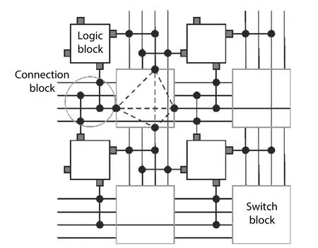
Fig. 1. Island-style architecture, which is the base of TM-ARCH with the time-multiplexed interconnects.
3. Target FPGA architecture
Fig. 1 illustrates an island-style FPGA, which is the base of our target time-multiplexed FPGA architecture. The only difference between this island-style architecture and ours is that all wires in our design can be time-multiplexed. In the conventional island-style FPGAs, vertical and horizontal routing channels surround logic blocks from all four sides containing multiple tracks. We define channel width as the total number of tracks in a channel. Every track has multiple wire segments. A switch block is arranged at every intersection of a vertical channel and a horizontal channel. Programmable switches are placed in switch blocks and connection blocks to implement configurable routing. Logic block pins are connected to routing channels through connection blocks.
3.1. Clock cycle and microcycle
In our new architecture, we divide a clock cycle into multiple microcycles. Different signals can occupy the same wire if this wire is multiplexable, and they can use the same wire at different microcycles in a clock cycle. We use a similar definition of microcycle and clock cycle as in Trimberger et al.’s work[2]. A clock cycle is constrained by the critical path delay.We defined Mc, which means a clock cycle has Mcmicrocycles.
3.2. Time-multiplexed wires
A route of nets is usually made up of many segments of wires. One segment of a wire can only be occupied between the time that the signal arrives and leaves in one clock cycle.In the TM-ARCH FPGAs, different signals can occupy the same segment of wires at different time if this wire segment can be multiplexed. Fig. 2(a) illustrates this. We first define that one clock cycle consists of two microcycles in this TM-ARCH architecture device. w1is multiplexable which is contained in both net N1and N2. This condition is permitted because N1and N2can use the same wire segment at different microcycles in one clock cycle. N1occupies this wire at [ T/4,T/3], which is in the first microcycle. N2occupies the wire segment at[2T/3,3T/4] in the second microcycle. Fig. 2(b) describes the time intervals in which N1and N2use the wire. T means the period of a clock cycle.
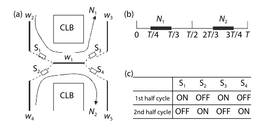
Fig. 2. (a) Signals N1 and N 2 occupy a wire at different time. (b) In time domain, N1 and N 2 do not overlap. (c) TM switches’ different states.
3.3. TM switch
A time-multiplexing switch (TM switch) is the key to implement time-multiplexing at the hardware level. Compared with conventional FPGAs, a TM switch has two more features:latching data and associating with multiple contexts.
3.3.1. Multiple contexts
In TM-ARCH, a TM switch can have at most Mccontexts.As time passes, the state of TM switch changes among the Mccontexts. This unique feature helps achieve the time-multiplexing of wires in our architecture. Fig. 2(c) shows an example of different states of TM switches (S1, S2, S3, and S4).This example can be time-multiplexed in the architecture shown in Fig. 2(a). In this condition, the TM switches can have two contexts, and change between them in one clock cycle.
3.3.2. Latching capability
A TM switch can latch the current logic value when it switches from on to off state. Fig. 2 illustrates the necessity of latching data. In the first microcycle, the state of TM switches S1and S3are on. This means the connection w2-w1-w3is maintained for the signal N1. In the second microcycle, TM switches S1and S3are turned off, while S2and S4are turned on. Hence, the connection w4-w1-w5is turned on while w2-w1-w3is turned off for the signal N2. In order to prevent w3from the floating state, the switch S3must to work as a driver. When it transits from on to off, S3will latch the current value, then drive the w3segment.
Francis’ architecture[9]can provide the latching capability, but it is provided by wires which are different from ours.Our architecture does not have to apply latches at LUT inputs, because our TM switches can provide the latching function.
4. Time-multiplexing-aware timing-drivenrouting algorithm
4.1. Problem formulation
G(V,E) is a routing-resource graph which is used to illustrate routing resources and their connections in TM-ARCH. V is the set of vertices (or nodes) which correspond to CLB pins or wires. The set of edges E corresponds to switches. During the association between every node and edge, there should be a delay time d . Capis the capacity of a node, which is defined as the maximum number for different nets that can occupy this node in one microcycle. We set Capequals to 1 for the nodes that correspond to the wires in our architecture.This is because at any microcycle a wire must be used by at most one net. Fig. 3 illustrates the routing-resource graph of a TM-ARCH device when Mc=2. The number listed next to the node name shows the capacity of this node. It should be noted that the sink and source are two different dummy nodes. A capacity of 2 is allocated to simulate the logical equivalence of the two input pins of a 2-input LUT.
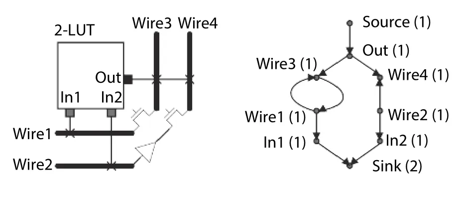
Fig. 3. Routing resource graph of TM-ARCH architecture.
For a signal i which is needed to be optimized in TMARCH, its net Nican be considered as a set of terminals, including source terminal Siand sink terminals Sij. Niconstitutes a subset of V. A routing solution for net Nican be considered as a directed routing tree R Tiembedded in G and connecting Siwith all Sij.
The router of TM-ARCH is designed for optimizing the circuit delay and routing all the nets at the same time. The router should identify and then schedule multiple qualified nets to a time-multiplex wire because the wire is time-multiplexed in TM-ARCH architecture.
4.2. Occupation bitmap
Our algorithm can identify a net (or a signal) that can be multiplexed to a wire with other signals. We record the time when a signal arrives and leaves. This helps us to get the signal’s occupation bitmap, which shows at which microcycle this signal may occupy this wire.
4.2.1. Arrival and leave time
A Maze router[23]is the core of our algorithm, the Pathfinder algorithm[24]and the VPR 5 algorithm. This router routes a net by wave-expanding from source and throughout the routing-resource graph until the wave-front reaches the sink of the net. It then back-traces the path and records it from its source to sink.
We compute two timing values: tarrivaland tleavefor a wire which is being expanded. tarrivalrecords when the signal arrives at this wire. Furthermore, tleaverecords when the signal leaves this wire. The two values can be denoted as:

In Eq. (1), the first item on the right side indicates the time needed from the source of net i to node n. The second item indicates the time when a signal arrives at the source of net i . In Eq. (2), dnis the delay of node n. The value of dnis illustrated in the FPGA architecture files from its manufacturer.We get the signal leave time by adding tarrivaland dn. In this work, we consider the delay as constant. All timing values in both equations are the maximum possible delay. We record the time that a signal arrives and leaves for every segment in the net. One wire may be included by the routes of multiple nets during the routing process. At this time, we record all the time that signal arrives and leaves from the wire.
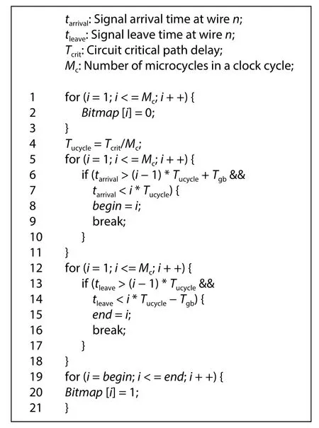
Fig. 4. Pseudo code for computing the occupation bitmaps.
4.2.2. Occupation bitmap
We can compute the occupation bitmap by using all the tarrivaland tleavevalues we record. This bitmap can be used to represent the occupation of a wire n by one net at different microcycles. The bitmap is an array that consists of Mcelements. Each element corresponds to one microcycle: the first element corresponds to the first microcycle, and the last element corresponds to the last microcycle.
Each element in the bitmap array can be 0 or 1. “1”means that the net uses the wire at the corresponding microcycle. “0” means that the net does not occupy.
We use the following function to calculate each element in the array,

We also use Tgbas the guard band for the skew of the microcycle clock network. The basic idea of this equation is that the net will only occupy this wire at a particular microcycle.
Fig. 4 gives the pseudo code for computing bitmaps. We first set all bitmap array elements to zero. Next, we compute which microcycle signal will arrive and give it to variable begin. Then we compute which microcycle signal will leave,and give it to a variable e nd. Finally, we assign all elements between b egin and e nd to 1, which means in these microcycles this net occupies the wire.
We also record the bitmap array for every wire in net i. Because we record the time when net i’s signal arrives and leaves the wire, we use these data to calculate the bitmap.We record multiple occupation bitmaps if this wire is occupied by the routes of multiple nets.
4.3. Congestion penalties at microcycles
Because wires in our architecture can be multiplexed by nets, our algorithm can record how many nets are currently using this wire at every microcycle by using the micro occupancy. This micro occupancy illustrates the degree of congestion at each microcycle for a wire. Our algorithm can compute the congestion penalties of wire at each microcycle based on its micro occupancy values when the wavefront arrives at the wire. Larger micro occupancy will cause larger congestion penalty.
4.3.1. Micro occupancy
Micro occupancy is a matrix that consists of Mcelements for each wire. Each element corresponds to one microcycle and takes an integer value, which means how many nets are currently occupying this wire at the corresponding microcycle.
Firstly we set all micro occupancy elements to zero.When wire n is included in the route of net i, the micro occupancy of n will be updated by the bitmap in section IV-B.

where j is in [ 1,Mc]. If the j -th element of bitmap is 1, it means this net uses this wire in the j-th microcycle and then j -th element of micro occupancy’s j-th element will be increased by one.
When a net i is being disassembled, the micro-occupation of all wires in the route of net i is updated.

where j is in [ 1,Mc]. Since this wire was used by net i in the jth microcycle, we should decrease the j-th element of micro occupancy by one.
4.3.2. Historical and present congestion penalty
With the records of micro occupancy, we can calculate the historical and present congestion penalties of a wire in each microcycle. The functions we use are shown as follows:

where j is in [ 1,Mc]. We will update p [j] for all wires affected if there still have any net disassembled like VPR. We also update h [j] of all wires only after one entire iteration.pfac
The routing schedule shows what and can be in each routing iteration. Table 1 illustrates the routing schedule which is also used in VPR 5.
4.4. Multiplexing-aware congestion cost
Cost calculation of multiplexing-aware congestion is an innovation of this algorithm. We do not consider it as congestion if a wire in our architecture is used by two more signals and they occupy the wire at different time.
Fig. 5 shows the pseudo code for computing congestion cost of wire in the wave expansion process. In this pseudocode, we should have already computed the bitmap array and the newest historical and present congestion penalties for every microcycle.

Table 1. Resource utilization of the system.
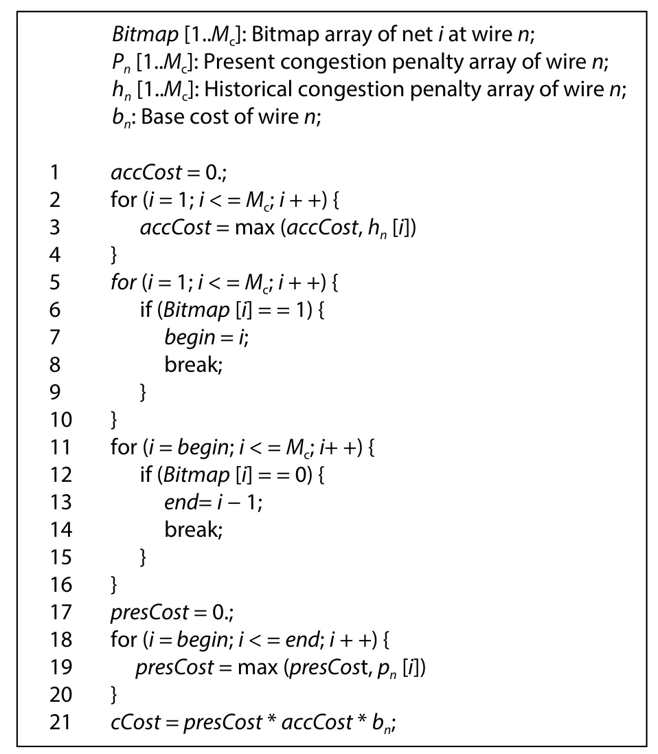
Fig. 5. Pseudo code for computing the congestion cost.
Lines 1–4 look for the largest historical congestion penalty. Lines 5–10 look for the position where the first “1” value is occurred in a bitmap, and save it to begin index. This means from which microcycle the wire starts to be occupied.Lines 11–16 saves the end index in a similar way, which means at which microcycle the wire occupation ends. Lines 17–20 record the largest present congestion penalty between the begin microcycle and end microcycle. Line 21 computes the overall congestion cost by multiplying the largest historical and present congestion penalties and the base cost of wire.

Eq. (9) is used after the VPR router obtains the new congestion cost. We use the largest historical congestion penalty in all microcycles as hnand use the largest present congestion penalty in the microcycles during which the wire is occupied.We only award the congestion of occupying wires in one net from the b egin -th microcycle until the e nd-th microcycle.
4.5. Overall cost function
The overcall cost function is the sum of two factors as in a VPR router. The first factor is the congestion sensitive cost,which is computed in Section 4.5. The second factor is the delay sensitive cost. We use the wire’s intrinsic delay as the delay cost and weighs the two parts based on timing criticality. Eq. (10) shows the overall cost function in our algorithm.
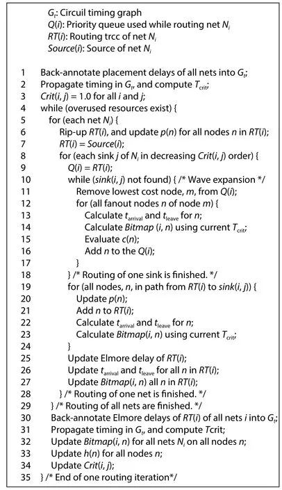
Fig. 6. Pseudo code for computing the congestion cost.

4.6. Legal routing solution
Our routing algorithm will check whether the current routing is effective after each iteration. If it is, our router iteration ends and keeps this solution. But if not, the router will start a new turn iteration.
A valid routing solution should not contain any overused routing resources. Although a wire can be multiplexed to be used by multiple nets, it is not overused as long as it is occupied by at most one net in any microcycle. Our router checks if Eq. (11) are met in every microcycle.

4.7. Pseudo code
Fig. 6 is the pseudo code of time-multiplexing-aware routing algorithm. For each signal in a net, we firstly use the maze router to route one signal from its source to sink over the routing-resource graph and record the path it has expanded. For each wire being expanded, we also record the arrival time and leave time to calculate the occupation bitmap.We use the bitmap to compute and update congestion penalties on this wire and then evaluates this wire's overall cost.We aim to decrease the criticality of the connection while doing the wave expansion. For all nodes in each net, we update its occupied time and Elmore delay after this net has been completely routed. After finishing routing all nets, we compute propagate timing in circuit timing graph and calculate critical path delay. If there is no more overused resources or reach the maximum number of iterations, the program will stop and return the final results.
Lines 6 and 20 show that this algorithm can compute the present congestion penalties at each microcycle for wires.Lines 14, 23, 27, 32 illustrate the fact that our algorithm can compute and update the occupation bitmap on wires. Lines 13, 22, and 26 are where our algorithm compute and update the time of signal arrival and leaving. Line 15 reflects the fact that this algorithm computes the time-multiplexing-aware congestion cost for a wire and then analyzes overall cost of this wire. Line 33 computes the historical congestion penalties at microcycles. Finally, line 4 checks the routing algorithm if there still have any remaining congested routing resources.This has been detailed in Section 4. In addition, our router can also check whether the next condition holds in every microcycle.
4.8. Algorithm analysis
In this part, we mainly focus on its unroutability detection, time complexity and memory requirement.
4.8.1. Unroutability detection
Our algorithm only declares the circuit is unroutable after 50 iterations on the given FPGA like Pathfinder algorithm. Because this process will take a long time, we will enhance our algorithm for quicker unroutability detection.
4.8.2. Time conplexity
The algorithm is based on iterations. In practice, the iteration number is usually limited to a certain number of times.Therefore, it is sufficient to analyze the iteration complexity in this algorithm.
The pseudo-code in Fig. 6 shows that, every iteration is made up of two parts. Netlist routing is the first (lines 5–29),and post-processing is the second (lines 30–34). Netlist routing means running routing algorithm for every net in netlist.Previous work shown that the complexity of the net routing algorithm in Pathfinder is O (k2log k)[3]. k means how many terminals does a net has. In the routing process, the extra computations included in our algorithm include computing signal’s arrival and leave times and then computing the occupation bitmap.
From Section 4.2, we know that the time consume on a routing-resource node n is constant. We also know that the complexity of computing bitmap is O (Mc). Mcmeans how many microcycles does one user’s clock cycle have. In our work, we limit Mcto 8. As a result, we consider it takes constant time to get the occupation bitmap. Taking the above into consideration, we can know that, for a k-terminal net, routing in our algorithm will typically take O (k2log k) time, which is same as in Pathfinder.
Next we will do post-processing. The main computation is computing Tcritby doing static timing analysis on timing graph in this part. We also used the critical path method(CPM) which is used in VPR 5 algorithm. Sapatnekar et al.[25]shown that the complexity of this algorithm is O (V+E). V means the vertices number in the circuit timing graph, and E means the edges number in the timing graph.
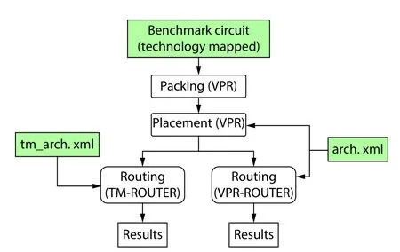
Fig. 7. (Color online) The TM-ARCH and TM-ROUTER evaluation framework.
Back-annotation Elmore delay (line 30) will take O(C)time for other operations in the post-processing portion,where C means how many connections between source and sink have in this circuit. Calculating occupation bitmap and updating historical congestion penalty of all nodes requires O(R) time. R represents the nodes number in routing-resource graph.
4.8.3. Memory requirement
In our algorithm, FPGA routing-resource graph and circuit timing graph are requiring a substantial amount of main memory requirement.
We record many information for all nodes in the routingresource graph, such as its connectivity information, physical information, congestion information, timing information and some other information used for wave expansion. O (R) is the memory requirement from routing-resource graph and R means nodes number in routing-resource graph.
We record the timing information and connectivity information for all vertex in timing graphs. For edges in timing graph, we record the timing information and connectivity information. Typically, O (V+E) is the memory requirement for timing graph. V in this means vertices number in the circuit timing graph, and E means edges number in the timing graph.
5. Algorithm validation
We verify our time-multiplexing-aware routing algorithm through experiments. By using this algorithm, we implement benchmark circuits for the TM-ARCH architecture. For comparison, we also implement the same set of benchmark circuits for conventional architectures. To achieve an easy and fair comparison, we use MCNC 20 benchmark circuits with a standard EDA flow.
5.1. Experimental setup
5.1.1. EDA flow
Fig. 7 shows our EDA flow. First, LUTs are packaged into the cluster logic block using the TVPack tool in the VPR 5 package. Next, place the circuit using VPR 5. The wiring is performed twice according to the same placement result. The VPR 5 timing-driven router is used to route circuits to traditional island FPGAs. TM-ARCH FPGAs with time-multiplexed interconnects are supported by our time-multiplexing-aware router. We call these two routing branches as conventional routing and time-multiplexing routing. Since then, we will call VPR timing-driven router and our time-multiplexing-aware router as VPR-ROUTER and TM-ROUTER.

Table 2. Main Features of Baseline FPGA Architecture.
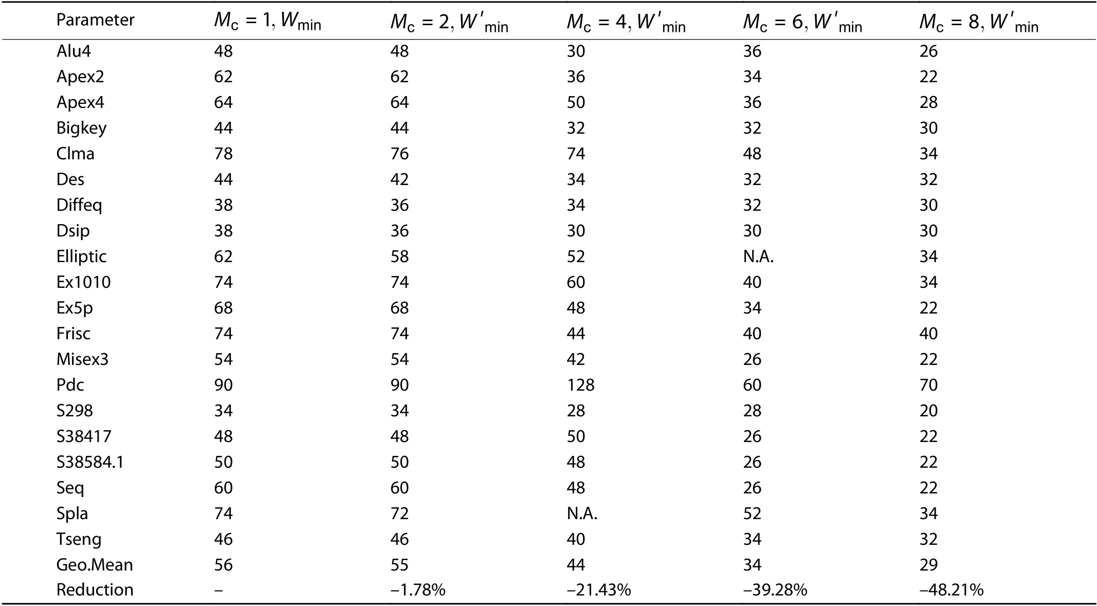
Mc Table 3. Minimum channel width for different values.
Mcis input to TM-ROUTER by command-line option. In our experiment, we restrict the value of Mcto be 2, 4, 6, or 8.We think 8 is a reasonable upper limit because of two reasons. First, a too large a Mcmeans a very high-frequency clock Clkf, because our architecture requires that frequency of Clkfshould be Mctimes the user’s clock. Second, too large a Mcwill result in a large amount of area overhead. It can be seen from the example implementation of the TM switch provided in the paper.
5.1.2. Assumptions of FPGA architecture
In this work, we only consider similar FPGA architectures.Even with this assumption, FPGA architecture’s design space is still quite large, so we cannot fully study the time-multiplexed interconnects. In order to make the work easier to do,we first fix a representative benchmark FPGA architecture.The benchmark FPGA architecture is represented in Fig. 7 as"arch.xml", which uses conventional interconnects. We replace all wires with our multiplexable wires, so we got the TM-ARCH FPGA architecture shown in Fig. 7 as "tm_arch.xml".
We choose the XML file used in iFAR[26]as the baseline FPGA architecture. Table 2 shows main features of this FPGA architecture.
5.2. Results
5.2.1. Minimum channel width
In this part of the experiments, a conventional routing and the time-multiplexing routing perform a binary search to find the minimum channel width for each circuit. VPRROUTER routes circuits to FPGA with conventional architecture to find the minimum channel width, and TM-ROUTER does the same work on TM-ARCH FPGA. We set 50 as the maximum iterations number for both routing algorithms.
Table 3 shows the minimum channel width experimental results. The numbers listed under “Wmin” column are the minimum channel widths routed by VPR-ROUTER in the conventional algorithm. Number listed undercolumn are that TM-ROUTER achieves for different Mcvalues. When Mc=2, TM-ARCH FPGA does not have advantages over conventional architecture. TM-ARCH FPGA achieve slightly better resultsfor only 5 circuits (des, diffeq, dsip, elliptic, and tseng) in 20 circuits. This result is counter-intuitive, because we expect TMARCH FPGA to result in the minimum channel width of all circuits.
Table 4. Percentages (%) of wire used in each individual microcycle for 20 benchmark circuits with
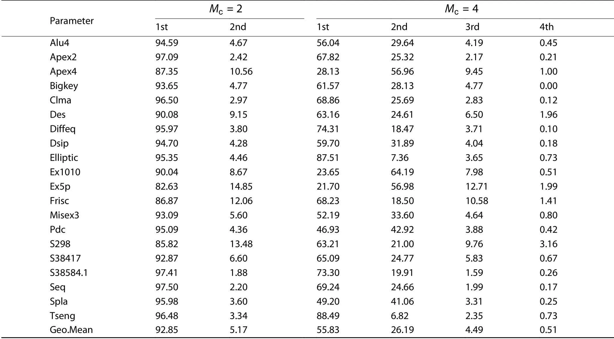
Table 4. Percentages (%) of wire used in each individual microcycle for 20 benchmark circuits with
Parameter Mc =2 Mc =4 1st 2nd 1st 2nd 3rd 4th Alu4 94.59 4.67 56.04 29.64 4.19 0.45 Apex2 97.09 2.42 67.82 25.32 2.17 0.21 Apex4 87.35 10.56 28.13 56.96 9.45 1.00 Bigkey 93.65 4.77 61.57 28.13 4.77 0.00 Clma 96.50 2.97 68.86 25.69 2.83 0.12 Des 90.08 9.15 63.16 24.61 6.50 1.96 Diffeq 95.97 3.80 74.31 18.47 3.71 0.10 Dsip 94.70 4.28 59.70 31.89 4.04 0.18 Elliptic 95.35 4.46 87.51 7.36 3.65 0.73 Ex1010 90.04 8.67 23.65 64.19 7.98 0.51 Ex5p 82.63 14.85 21.70 56.98 12.71 1.99 Frisc 86.87 12.06 68.23 18.50 10.58 1.41 Misex3 93.09 5.60 52.19 33.60 4.64 0.80 Pdc 95.09 4.36 46.93 42.92 3.88 0.42 S298 85.82 13.48 63.21 21.00 9.76 3.16 S38417 92.87 6.60 65.09 24.77 5.83 0.67 S38584.1 97.41 1.88 73.30 19.91 1.59 0.26 Seq 97.50 2.20 69.24 24.66 1.99 0.17 Spla 95.98 3.60 49.20 41.06 3.31 0.25 Tseng 96.48 3.34 88.49 6.82 2.35 0.73 Geo.Mean 92.85 5.17 55.83 26.19 4.49 0.51
We think that, in one clock cycle there are two microcycles that can only supplies little opportunity to TM-ROUTER to achieve time multiplexing of wires. Table 4, “Mc=2” list s the wire percentage used in the first two microcycles for MCNC 20 benchmark circuits, when we divide a clock cycle into two microcycles. The data are generated in the manner as follows. We adjust VPR-ROUTER codes in order to record the time when the signal occupies wire to the result. Then we start VPR-ROUTER routing process with the minimum channel width listed in Table 3 column “Wmin”. After that, we use a program to analyze the results and determine which microcycle each line segment is used in according to Eq. (3). The program also counts the portion of wires used in each microcycle in the final routing.
Table 4 shows that, in the first microcycle, 92.85% of the wires are used, while in the second microcycle, only 5.17%wires are used. This means that TM-ROUTER has very limited opportunities for time-multiplexing in this condition. To implement time-multiplexing in FPGAs, our routing algorithm will match the same wire in the first microcycle and the second microcycle. Table 4 shows that used wire segments are most likely to be used by net in the first microcycle, and less likely to be used by another net in the second microcycle, so our time-multiplexing-aware algorithm may less likely to implement time-multiplexing wires in this situation. Looking back at Section 4, the signal does not be actively delayed by our routing algorithm. But scheduling algorithm of Francis et al’s does it to implement more time-multiplexing[9]. We can see that, when a clock cycle is divided into four microcycles, Table 4, column “Mc=4”, tabulates the microcycle distribution using the wires. The process of generating these data is similar to for Mc=2. In this condition, the distribution between the first and second microcycle seems more balanced than when Mc=2. This gives TM-ROUTER more opportunities to implement time-multiplexing.
TM-ARCH generally needs a smaller channel width from Mc= 4. This follows our expectations that multiplex can lead to minimum channel width reduction. The result will be more significant when the division of microcycle is more detailed:the reduction of minimum channel width is 19.86% (Mc=4),37.74% (Mc=6) , and 47.89% (Mc=8) . With Mcincreases,one wire can be multiplexed by more nets, so fewer wires are required to route a given number of nets.
5.2.2. Circuit critical path delay
FPGAs routing resources are often not heavily utilized in order to reduce latency in real applications. So we use 20%more minimum channel width than Table 3 to do the routing process. In this section, we also assume that TM switch has same delay with its conventional switch.
Table 5 lists the critical path delays with low-stress rout-ing for 20 benchmark circuits. “Tcrit” column is the result of the conventional architecture, while thecolumns is the result the TM-ARCH architecture. When Mc=2, the critical path delay of TM-ARCH is slightly larger (1.13%) and the channel width used is slightly smaller (4.08%). However, when Mc= 4, 6, and 8, the channel width uses by TM-ROUTER is reduced by 19.69%, 37.87%, and 46.97%. Moreover, the critical path delay of TM-ROUTER can be moderately reduced: 1.79%,3.84%, and 1.28%.
In conventional FPGAs, circuit critical path may not be routed in the shortest path due to limited routing. This is true even when low-stress wiring is performed. Unlike conventional FPGAs, the TM-ARCH architecture allows multiple signals multiplex wires in different clock cycles. This effectively mitigates its routing congestion. As a result, the circuit critical pathis likely to be routed in a shorter path.
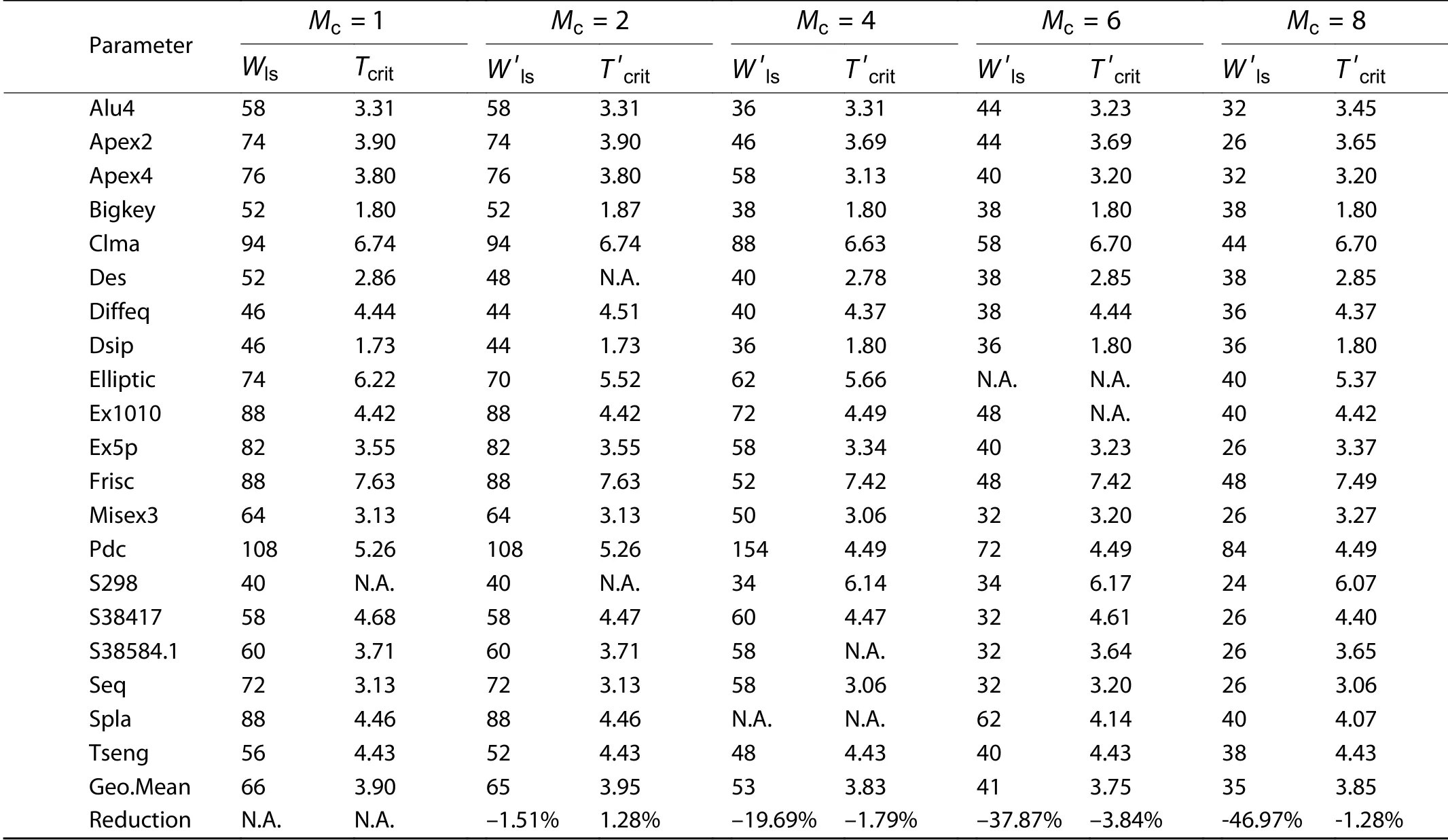
Table 5. Minimum channel width for different M c values.
6. Conclusion
In this paper we propose a time-multiplexing FPGA architecture and its routing algorithm. Our algorithm actively identifies the qualified interconnects that can be multiplexed on our new FPGA architecture. We have validated the architecture and algorithm by implementing it as a multiplexingaware router and using this router to implement benchmark circuits to FPGAs with time-multiplexed interconnects. The results show that compared with an existing router targeting a conventional island-style architecture, 38% smaller minimum channel width and 3.8% smaller circuit critical path delay can be achieved.
杂志排行
Journal of Semiconductors的其它文章
- Optimizing energy efficiency of CNN-based object detection with dynamic voltage and frequency scaling
- Towards high performance low bitwidth training for deep neural networks
- Towards efficient deep neural network training by FPGA-based batch-level parallelism
- HRM: H-tree based reconfiguration mechanism in reconfigurable homogeneous PE array
- Accelerating hybrid and compact neural networks targeting perception and control domains with coarse-grained dataflow reconfiguration
- A survey of neural network accelerator with software development environments
